Dottorato di Ricerca in Ingegneria Elettronica,
Informatica e delle Telecomunicazioni
XX Ciclo
ING-INF/01
Exploration of Communication
Strategies for Computation
Intensive Systems-On-Chip
Tesi di Dottorato di Relatore
Antonio Deledda
Chiar. mo Prof.Roberto Guerrieri
Coordinatore Chiar. mo Prof.Paolo Bassi
Keywords:
Reconfigurable architectures
Heterogeneous MPSoC
MORPHEUS
Network On Chip
Digital Signal Processing
Contents
List of Figures ... v
List of Tables... ix
Introduction ... 1
Chapter 1 Multiprocessing and Reconfigurable Computing ... 5
1.1 MPSoC state of the art... 7
1.1.1 TI OMAPTM... 8
1.1.2 ST NomadikTM ... 9
1.1.3 Philips NexperiaTM ... 10
1.2 Reconfigurable computing ... 12
1.2.1 Run-time reconfigurable instruction set processors ... 14
1.2.2 Coarse grained reconfigurable processors... 20
1.3 Interconnection Strategies ... 24
1.4 General Outline of the MORPHEUS solution ... 26
Chapter 2 The MORPHEUS Design... 31
2.1 The MORPHEUS Reference Architecture... 31
2.1.1 ARM926EJ-S Embedded processor ... 34
2.1.2 Multi-Layer AMBA bus system... 36
2.1.3 DesignWare DW_ahb_dmac DMA Controller ... 38
2.1.4 Interrupt Controller... 41
2.1.5 MORPHEUS IO Peripheral Set ... 42
2.2.1 XPP...45
2.2.2 PiCoGA ...62
2.2.3 Embedded FPGA...75
Chapter 3 Memory Subsystem Definition ...87
3.1 Level 3: Off-Chip Memory...90
3.2 Level 2: On-Chip Memory ...92
3.3 Level 1: Data/configuration exchange buffer...96
3.3.1 PiCoGA integration: The DREAM Architecture ...98
3.3.2 M2000 Integration ...106
Chapter 4 Interconnect strategy...117
4.1 Handling of micro-operands: local HRE interconnect strategy deployment ...118
4.2 Handling of Macro-operands: Global Interconnect strategy deployment ...120
4.3 Chip level Interconnect strategy deployment ...122
4.4 Communication Kernel (Network-on-chip) ...122
4.4.1 Communication infrastructure...124
4.4.2 The “load-α store-β” communication pattern ...125
4.4.3 Communication granularity...127
4.4.4 Chip level Interconnect strategy deployment ...128
4.4.5 Programming NoC Transfers: ...130
4.4.6 Programming NoC Space address ...138
4.5 Results and Bandwidth Estimation...141
4.5.1 Bandwidth Analysis...142
4.5.2 Conclusion ...145
Chapter 5 Overall Implementation Results ...147
5.1 Overall Chip description...150
5.2 Processor Based Infrastructure ...154
5.2.2 AMBA Subsystem... 155
5.3 Hardware Services... 157
5.3.1 The Predictive Configuration Manager block ... 157
5.3.2 The CMC DDRAM Memory Controller... 158
5.4 The Data Interconnect Infrastructure ... 159
5.5 Heterogeneous Reconfigurable Engines (HREs) ... 164
5.5.1 DREAM... 164 5.5.2 M2000 ... 167 5.5.3 Pact XPP... 169 5.6 Padframe... 171 5.7 Final Consideration ... 172 Conclusion... 175 Bibliography... 177
List of Figures
Figure 1: Computational requirements vs. Moore’s law and battery
storage... 2
Figure 2: MPSoC trends ... 5
Figure 3: TI OMAP 3430 block diagram ... 8
Figure 4: ST Nomadik multimedia processor architecture... 9
Figure 5: Philips Nexperia PNX1500 block diagram ... 11
Figure 6: P-RISC Architecture ... 15
Figure 7 :GARP Architecture ... 16
Figure 8: MOLEN Architecture... 18
Figure 9: PACT Archiecture... 22
Figure 10: Morphosys Architecture... 23
Figure 11: Architecture of a Heterogeneous reconfigurable device... 27
Figure 12: Morpheus Overall Architecture... 32
Figure 13: ARM926EJ-S block diagram ... 35
Figure 14: MORPHEUS multilayer bus hierarchy... 37
Figure 15: Scheme of a cross-layer DMA transfer... 39
Figure 16: DMA transfer hierarchy ... 40
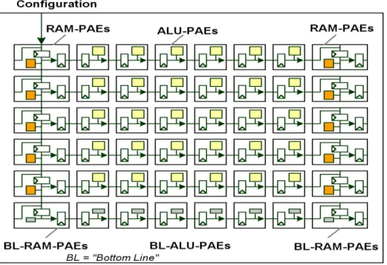
Figure 17: An XPP array with 6x5 ALU-PAEs ... 46
Figure 18: FNC-PAE ... 48
Figure 19: A sample XPP -array (6x5 ALU PAEs)... 49
Figure 20: ALU PAE objects... 50
Figure 21: RAM PAE objects with I/O ... 51
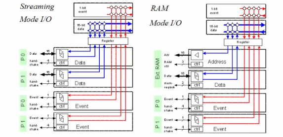
Figure 22: XPP I/O in Streaming mode & RAM mode... 52
Figure 23: FNC-PAE overview the ALU data-path ... 53
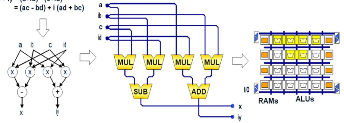
Figure 24: Configuration chain... 56 Figure 25: Flow-graph of a complex multiplication and spatial
Figure 27: Pipelined DFG in PiCoGA... 65
Figure 28: Example of PGAOP mapping on PiCoGA ... 67
Figure 29: Reconfigurable Logic Cell: simplified architecture ... 68
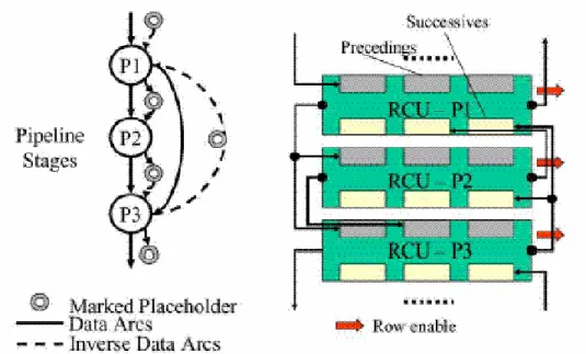
Figure 30: Pipeline management using RCUs ... 71
Figure 31: Basic operations in Griffy-C ... 73
Figure 32: FlexEOS macro block diagram ... 76
Figure 33: MFC schematic ... 78
Figure 34: MAC schematic... 81
Figure 35: Full crossbar switch... 82
Figure 36: FlexEOS core architecture ... 83
Figure 37: MORPHEUS SoC architecture ... 87
Figure 38: Data Storage Hierarchy ... 96
Figure 39. DREAM architecture... 98
Figure 40. RLC in the DREAM reconfigurable data path. ... 101
Figure 41. Integration of the address generators in DREAM architecture... 103
Figure 42. Classification of the available data patterns. ... 103
Figure 43. Throughput vs interleaving factor. ... 105
Figure 44: M2000 HRE sub-block as inserted in the top design ... 106
Figure 45: M2000 sub-block memory maps... 107
Figure 46: DEB I/O signals ... 108
Figure 47: DEB Control Registers... 109
Figure 48: M2000 input/output pad distribution... 110
Figure 49: Proposed NoC Topology... 123
Figure 50: HRE and Target Network interfaces ... 126
Figure 51: Multi-block Transfer with Source and Destination Address Auto-reloaded ... 135
Figure 52: NoC Programming Space address... 139
Figure 53: Throughput in MByte/s in a best case scenario... 144
Figure 55: Schematic description of the MORPHEUS communication
infrastructure... 159
Figure 56: Description of the DREAM Architecture ... 164
Figure 57: Block diagram of the M2000 HRE ... 167
List of Tables
Table 1: DesignWare DMA Bandwidth estimation... 40
Table 2: XPP-III array preliminary characteristics... 57
Table 3: XPP-III array hardware IP parameters ... 58
Table 4: eDRAM size and configuration options ... 80
Table 5: FlexEOS 4K-MFC features and size ... 84
Table 6: Example of design mapping results... 85
Table 7: Distribution of data flows inside MORPHEUS architecture... 89
Table 8: DREAM Application Program Interface... 99
Table 9: Programming Registers for NoC Transfers ... 131
Table 10: Interrupt Register connection scheme ... 140
Table 11: Application Bandwidth Requirements ... 142
Table 12: Bandwidth estimation (MB/s) ... 143
Table 13: Top Entity Pinout ... 152
Table 14: Area of the ARM component ... 154
Table 15: Rough Power Consumption estimations for the ARM926 core ... 155
Table 16: Gate Count for the AMBA subsystem components ... 155
Table 17: Gate Count for the AMBA subsystem components ... 156
Table 18: Area occupation of memory cuts included in the AMBA bus system design... 156
Table 19: Rough Power Consumption estimations for the AMBA Subsystem ... 156
Table 20: Area occupation for the PCM... 157
Table 21: Rough Power Consumption estimations for the PCM ... 157
Table 22: Main Building blocks of the CMC controller... 158
Table 25: Area occupation of main blocks composing the
communication infrastructure ... 162 Table 26: Area occupation of STNoC IPs ... 162 Table 27: Gate count of the main RTL sub-blocks composing DREAM.. 165 Table 28: Area of the hard macro blocks composing DREAM... 165 Table 29: Main contributions to the estimated Power consumption of
DREAM ... 166 Table 30: Gate count of the main RTL sub-blocks composing the
M2000 HRE ... 168 Table 31: Area of the hard macro blocks composing the M2000 HRE... 168 Table 32: Main contributions to the estimated power consumption of
the M2000 HRE ... 169 Table 33: Area estimations of the main blocks connecting the XPP
Macro to the Morpheus System ... 170 Table 34: Rough power consumption evaluations for the
XPP/Morpheus connection ... 170 Table 35: Estimation of the area occupation of the main blocks
composing the XPP... 171 Table 36: Rough power consumption estimation for the IO Ring... 172 Table 37: Main contributions to overall chip area ... 173
Introduction
Data intensive processing in embedded systems is receiving relevant attention, due to rapid advancements in multimedia computing and high-speed telecommunications. Applications demand high performance under realtime requirements, and computation power appetite soars faster than Moore’s law (see Figure 1, [13]). Processor efficiency is impaired by the memory bandwidth problem of traditional Von Neumann architectures. On the other hand, the conventional way to boost performance through Application Specific Integrated Circuits (ASIC) suffers from sky-rocketing manufacturing costs and long design development cycles. This results in an increasing need of post-fabrication programmability at both software and hardware level. Field Programmable Gate Arrays (FPGA) bring maximum flexibility with their fine grain architecture, but imply severe overheads in timing, area and consumption. Word or sub-word oriented Run-time Reconfigurable Architectures (RAs) [1] offer highly parallel, scalable solutions combining hardware performance with software flexibility. Their coarser granularity reduces area, delay, power consumption and reconfiguration time, but introduces tradeoffs in the design of the processing elements, that need to be tailored for a given application domain.
A possible way to mitigate this aspect for building a flexible yet efficient signal processor is to substitute each ASIC accelerator with a specific domain oriented RAs, inducing a graceful shift of SoCs from application specific circuits to domain oriented platforms, where different flavors of reconfigurable hardware, each more suited to a given application environment, are merged with ASIC and general purpose processors to provide ideal tradeoff between performance and post-fabrication programmability. The immediate advantage is that the higher computational density of RAs allows to build networks composed of a significantly smaller number of nodes. The immediate
Figure 1: Computational requirements vs. Moore’s law and battery storage provide independent application mapping styles and entry languages. In this context, critical issues are related to the definition of
• a toolset that must be capable to hide RA heterogeneity and hardware details providing a consistent and homogeneous programming model to the end user
• a data interconnect infrastructure, that must sustain the bandwidth requirements of the computation units while retaining a sufficient level of programmability to be adapted to all the different data flows defined over the architecture in its lifetime.
These aspects are strictly correlated and their combination, together with the strategy deployed for RA computation synchronization represents the signal processor interface toward the end-user. In particular, the architecture view
model looking like purely functional code. Program parts requiring acceleration on RAs should be identifiable in the easiest possible way. A toolset can then handle and program the code corresponding to data movements and reconfigurations related to these accelerating parts.
In this context not only computation but also communication aspects must indeed be considered. This will enable performance optimization by masking communication time by computation time through a “pipelined” behavior. The scheduling of these accelerating parts among each other, including loading configuration and execution, may be managed at compilation time based on RTOS-oriented services.
This thesis presents the definition and the design of a heterogeneous reconfigurable SoC platform, where state-of-the-art RAs of different size and nature are grouped together in a processor-controlled system. In particular, this work aims at describing the most significant challenges and design choices that have been faced in the deployment of a well known NoC infrastructure (the ST Spidergon NoC approach [2]) and the consequent impact on the architecture and toolset definition. I believe that the most relevant innovation aspects of this work are:
1. A significant milestone in the field of Heterogeneous-MultiCore SoCs;
2. The first design-case challenging the deployment of the NoC concept to a network of high-bandwidth computation intensive RAs. The rest of this thesis is organized as follow. In Chapter 1, the terminology and basic foundation of Computation Intensive System-on-Chips are revisited to pave way to the rest of the thesis. An overview of the European project, where this work was done, is also given. Chapter 2 presents the defined architecture for the MORPHEUS project. Chapter 3 and 4 details the main choices given in the definition of the memory hierarchy and the adopted communication
infrastructure. The last chapter presents design and performance results achieved in the frame of this project.
Chapter 1 Multiprocessing and
Reconfigurable Computing
Up to the 1990s processor designers mainly focused their work on boosting single processor performance. This evolution was conducted constantly increasing clock rates extending instruction-level parallelism (ILP). This was made possible by technology scaling which reduced physical delays and device sizes allowing for a larger area to be utilized by new logic. The result is a variety of superscalar architectures employing different hardware solutions to concurrently process different instructions. Performance of future embedded systems, according to the ITRS estimation shown in figure 1.1, will require the execution of an increasing number of instructions per clock cycle, but the cost of extracting such parallelism from a single thread is becoming prohibitive both in terms of area and energy consumption.
It has nevertheless been stated that trying to further increase ILP is not the best choice as explained by D. Patterson in [17]. As an alternative to superscalar architectures, processor designers and researchers are proposing a different approaches based on Tread Level Parallelism (also named Task Level Parallelism, TLP) that seem to enable significant speed-up and proves more flexible than ILP.
From an architecture point of view, we can distinguish MPSoC architectures in two main classes:
1. Homogeneous MPSoC, where all the processing elements are usually identical or at least share a common ISA,
2. Heterogeneous MPSoC, characterized by the integration of different computational core: i.e. processor with different ISAs, several ASICs or DSPs, etc.
One of the main aspects in heterogeneous MPSoC is that software modules have to interrelate with hardware modules. In [18] the authors show the use of an high level programming approach for the abstraction of HW-SW interfaces. The proposed programming model is based on a set of functions (primitives) that can be used by the SW engineer to interact with HW modules. In the reconfigurable computing domain, alternative approaches have also been investigated; in [19] a scalable programming model (named SCORE) is presented and used for a homogeneous scalable reconfigurable architecture. The model allows indifferently computing a set of tasks in time or in space, following the resources available: the advantage is that software is reusable for any generation of component based on that model.
From the memory point o view we can investigate two main programming models:
1. SMP (Symmetric Multi Processing) where all the processors have a global vision of the memory (shared memory) and
2. AMP (Asymmetric Multi Processing) where the processors are loosely coupled and have generally dedicated local memory resources.
Task control management is also an issue to consider. Threads can be handled at execution time (dynamically on a single processor) by an operating system or at design time (statically) by complex scheduling techniques. A part of the MP-SOC community focuses on static task placement and scheduling in MP-SOC. Indeed, having a complex operating system in memory taking care of run-time mapping is often not feasible for a SOC, because of the restricted memory resources and associated performance overhead. Moreover, these systems are often heterogeneous and dedicated to a few tasks, and a single but efficient scheduling of tasks may be more adapted. For instance in [20], the authors summarize the existing techniques (ILP based or heuristics) and have developed a new framework based on ILP solvers and constraint programming to solve at design time the task allocation/scheduling problem.
1.1 MPSoC state of the art
Multiprocessor systems-on-chip are mostly suitable for high-volume products with stringent constraints in terms of performance, power consumption and cost. Many application domains are covered by these features, including multimedia, communications, automotive and networking. This section, referring to a survey proposed by Wolf [16], describes some state-of-the-art MPSoCs, suitable for different application domains. A common feature of all the analyzed architectures resides in the integration of a standard processor which operates as the main system controller. This choice generally simplifies system programmability allowing multiple processing elements and customized ASIC blocks to be programmed as co-processors, maintaining a central control task on the control processor.
1.1.1 TI OMAP
TMThe Open Multimedia Application Platform (OMAP) [21][22] proposed by Texas Instruments is a combined RISC/DSP architecture targeted to 3G wireless applications. The platform supports mainly baseband processing and voice services, in addition multimedia, gaming and other application at user level.
Figure 3: TI OMAP 3430 block diagram
Figure 3 shows the architecture overview of the TI OMAP 3430. The inclusion of a standard ARM Cortex A8 processor ensures the compatibility with different commercial operating systems, while the additional DSPs provide the platform with additional computational power to process the previously cited applications. The ARM core and the DSP use a shared external DRAM interface, while a consistent amount of SRAM are internally integrated. A complete set of peripherals is also included (USB, I2C, UARTs,
GPIOs). Outstanding gaming capabilities will also be possible, thanks to ARM’s integrated vector floating-point acceleration working with a dedicated 2D/3D graphics hardware accelerator.
To simplify software development on the heterogeneous multi-core architecture, the RISC is defined as the system master and a DSP resource manager runs on the ARM. Tasks executed on the DSP are controlled through a DSP/BIOSTM bridge which adds support for inter-processor communication,
based upon the mailbox mechanism. The DSP/BIOS allows the ARM to initiate DSP tasks, to exchange messages and data streams with the DSP and to control the DSP status. This hardware support simplifies system programmability treating the DSP and the accelerators as system co-processors.
1.1.2 ST Nomadik
TMSTMicroelectronics Nomadik platform [23] is designed for 2.5G/3G mobile phones, personal digital assistants (PDAs) and, more in general, portable wireless products with multimedia capabilities. The architecture is focused at delivering ultra low power consumption enabling audio and video applications. The result is a 20mW typical power consumption with the computational power required by MPEG-4 encoding and decoding with display sizes ranging from 160x160 pixels to 640x480 pixels.
Figure 4: ST Nomadik multimedia processor architecture
enabling the user to trade off between high performance and high code density. The cached ARM CPU features a memory management unit (MMU) and is clocked at a frequency up to 350 MHz. It has a 16-Kbyte instruction cache, a 16-Kbyte data cache, and a 128-Kbyte level 2 cache, and supports the Jazelle™ extensions for Java acceleration.
In addition to the ARM core a series of accelerators are included for dedicated task:
• smart video accelerator for SDTV video encoding and decoding, with MIPI and SMIA camera interfaces.
• smart audio accelerator containing a comprehensive set of digital audio decoders and encoders, and offering a large number of 3-D surround effects.
• A smart imaging accelerator, providing real-time, programmable image reconstruction engine.
• A smart graphics accelerator
A multi-layer AMBA crossbar interconnect for optimized data transfers between the CPU, accelerators, memory devices and peripherals is also integrated. A set of hardware semaphores for flexible inter-process management is used. A wide range of peripheral interfaces (GPIO, USB-OTG high speed, UART, I²C, FIrDA, SD/high-speed MMC/Memory Stick Pro, fast serial ports, TV output, color LCD and camera interfaces, scroll-key encoder, key-pad scanner) is available.
1.1.3 Philips Nexperia
TMThe Nexperia NXP1500 [24] is a MPSoC architecture developed by Philips Semiconductors and designed for digital video applications, including digital television, home gateway and networking, and set-top box applications.
At the heart of all PNX1500 processors is a TriMedia TM3260 CPU core delivering top performance through the implementation of a very-long instruction word (VLIW) architecture. Five issue slots enable up to five simultaneous RISC-like operations to be scheduled into only one VLIW instruction. These operations can simultaneously run on five of the CPU’s 31 pipelined functional units within one clock cycle.
Figure 5: Philips Nexperia PNX1500 block diagram
In addition to the Trimedia core a set of specific accelerators are integrated. A video input processor (VIP) captures and processes digital video for use by
crop, horizontally down-scale, or convert the YUV video to one of many standard pixel formats as needed before writing data to memory. An additional versatile, programmable memory-based scaler unit applies a wide variety of image size, color, and format manipulations to improve video quality and prepare it for display.
A set of Audio input/output programmable device are also integrated. Audio units provide all signals needed to read and write digital audio datastreams from/to most high-quality, low-cost serial audio oversampling A/D and D/A converters and codecs. The AI unit supports capture of up to eight channels of stereo audio. The AO unit outputs up to eight channels and directly drives up to four external, stereo I2S or similar D/A converters or highly integrated PC
codecs. Additional On-chip hardware accelerators are targeted to 2D and 3D graphics processing, MPEG decoding, image scaling and filtering, and display channel composition. All coprocessors read input and write results to memory.
A PNX1500’s CPU and processing units access external memory through an internal bus system comprising separate 64-bit data and 32-bit address buses. Arbitrated by the MMI unit (Main Memory Interface), the internal buses maintain real-time responsiveness in a variety of applications. The system also includes an external DRAM interface, a DMA for each processor and several I/O interfaces.
1.2 Reconfigurable computing
The first idea of a reconfigurable computing machine was conceived by Gerald Estrin in the early 1960s [30] when he presented the “fixed plus variable structure computer” [31]. It would consist of a standard processor, augmented by an array of reconfigurable hardware blocks controlled by the main processor. The reconfigurable hardware could be programmed to perform a specific task with performance comparable to a dedicated hardware block.
perform a new different task. This first example of hybrid computer, combining the flexibility of a software programmable processor core with the performance of dedicated hardware, failed to become an interesting solution for commercial products. For many years, in fact, microprocessors combined with Application Specific Integrated Circuits (ASICs) have represented a state of the art solution able to meet application requirements when stand alone processor computational power was not adequate.
The combination of higher silicon integration degree and the need of flexibility imposed by the continuous algorithmic innovation, has generated a tremendous attention on the reconfigurable computing. The term
Reconfigurable Computing (RC) is broadly intended as the capability to couple
software based programmability with dynamic hardware programmability. The most common devices utilized as reconfigurable units are the Field Programmable Gate Arrays (FPGAs), but current scenario of reconfigurable devices is being crowded by a variety of reconfigurable architectures, with different reconfiguration granularities (coarse/fine/mixed grain fabrics), VLIW processing, systolic arrays, processor networks and so on. RC has long been considered [27][28][29][32][33][34][35][36] a feasible alternative to tackle the requirements described before. As shown in [28][29][36][37][38], reconfigurable architectures are classified depending on their grain, intended as the bitwidth of their interconnect structure and the complexity of their reconfigurable processing elements (PEs). Field Programmable Gate Arrays (FPGAs) are typically regular architectures where PEs are based on lookup tables (LUTs) and merged in a bit-oriented interconnect infrastructure. Featuring small LUT cells and 1-bit interconnect FPGAs are typically described as fine-grained. Their very symmetrical and distributed nature makes FPGAs very flexible and general purpose, and they can be used to tackle both computation-intensive and control-oriented tasks, to the point that large commercial FPGAs are often used to build complete Systems-On-Programmable-Chip (SoPCs) [39]. Arithmetic-oriented datapaths feature
possible to achieve higher efficiency designing PEs composed of hardwired operators such as ALUs, multipliers or multiplexers. Such kind of archietcture are usually defined coarse-grained. These devices trade part of the flexibility of FPGAs in order to provide higher performance for specific computations. There exist also a set of devices that fall in between the above two classifications, featuring bit widths of 2 or 4 bits, and small computational blocks that are either large LUTS or small arithmetic blocks as 4-bits ALUs. These can be classified as medium-grained.
All this broad category of digital architectures fall under the cumulative name of “Reconfigurable Architectures” (RAs), underlining their capability to reconfigure at execution time part of their hardware structure to support more efficiently the running application. In this broad domain, we use the definition
“Reconfigurable Instruction Set Processor (RISP)” for those reconfigurable
architectures that are tightly integrated in order to compute as a single adaptive processing unit according to the Athanas/Silverman paradigm [25] regardless of their hybrid nature. The next two sections will describe the evolution of the reconfigurable processor concept in the last 10 years, through the description of several significant contributions in the field by both industry and academia.
1.2.1 Run-time reconfigurable instruction set processors
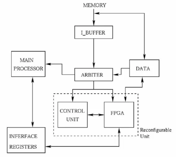
The first significant attempt at deploying instruction set metamorphosis to embedded systems taking advantage of run-time configurable hardware is P-RISC (PRogrammable Instruction Set Computer), proposed by Razdan/Smith in 1994 [26]. The architecture is depicted in Figure 9.3.
The PRISC micro-architecture is composed of a fixed RISC (a MIPS core) extended by instructions mapped on a standard FPGA embedded in the core and defined as a PFU (Programmable Function Unit). An efficient interface between the core and the PFU aims to fit the PFU into the core pipeline.
Figure 6: P-RISC Architecture
A compilation model for the ISA extension, starting from C specification is also proposed. To ease the physical interface between core and extension and to define a clear programming pattern for the compiler-based extraction of “interesting” extensions each PFU can handle 2-inputs 1-output functions. The most interesting concept of this architecture is that the PFU is considered as a function unit of the datapath, similar to an additional ALU, and PFU operands are read and written through the core register file providing a tightly coupled model. This is very friendly from the compiler and programmer point of view.
A significant novel step is represented by the “GARP” processor, which is shown in Figure 9.4. GARP [40] couples a MIPS core with a custom designed reconfigurable unit, connected as a coprocessor and addressed with explicit
Move instructions while specific assembly instructions are implemented to
trigger the configuration and computation on the reconfigurable unit. Unlike in the architecture P-RISC, the granularity of tasks mapped on the unit is quite coarse, to fully exploit the potentiality of the space-based computation approach. Another main difference respect the previous approach is that the
to the extension unit than that allowed by the core register file, although it raises relevant issues regarding memory access coherency.
Figure 7 :GARP Architecture
The GARP reconfigurable unit is composed of an array of 24 rows of 32 LUT-based logic elements. Fast carry chains are implemented row-wide to provide efficient 32-bit arithmetical/logical operations on a single row. Each row can be approximated to a 32-bit ALU and an embedded hardware
sequencer is added to the unit, in order to activate operators (one for each row)
with appropriate timing to build a customized pipeline. Candidate kernels are described at C-level and decomposed in Data-Flow-Graphs (DFG), determining elementary operators and their data dependencies, and then mapped over the existing LUT resources. The sequencer embedded in the
very well with C language and the GARP C compiler, thus easing a lot the gap between software and hardware programming indicated by Athanas/Silverman as the key issue in the deployment of instruction set adaptivity.
The MOLEN polymorphic processor [41] can be considered another important example of the reconfigurable instruction set processor paradigm. It has been implemented on a Xilinx Virtex-II FPGA coupling the on-chip PowerPC microprocessor with the Xilinx reconfigurable fabric, but the approach is quite independent from the device used to prove its feasibility. The significant contribution of MOLEN does not reside in its physical implementation, but in the theoretical approach to HW/SW co-processing and micro-architecture definition. The MOLEN contribution can be described as
• A microcode-based approach to the reconfigurable processor microarchitecture
• A novel processor organization and programming paradigm • A compiler methodology for code optimization
A significant difference with all previously described architectures is that MOLEN does not attempt to propose a mean for “hardware/software co-compilation”. Tasks to be mapped on the programmable hardware unit are considered as atomic tasks, primitive operations Microcoded in the processor architecture. Instruction set extensions are defined separately as libraries with an orthogonal HDL-based flow. Designing microcode for the adaptive extensions (_µ-code) consists in HDL design, synthesis and place & route of the extension functionality over third-party tools without any assistance from the reconfigurable processor compilation environment. This could raise issues for algorithmic developers not proficient with hardware design. On the other hand, this choice allows a large degree of freedom in the implementation allowing to extend the basic concepts to any technology. Also, as described in [41], the microcoded approach allows MOLEN-based RISPs to achieve
according to Amdahl’s law, much higher than speedups achieved by hybrid compilation.
Figure 8: MOLEN Architecture
The MOLEN micro-architecture, shown in Figure 9.5., is organized as follows: instructions are decoded by an arbiter determining which unit is targeted. “Standard” instructions are computed by the Core Processor while instructions targeting the reconfigurable hardware are computed on the
Reconfigurable Processor which is composed of a computational unit called
Custom Configured Unit and a reconfigurable microcode control unit. The
control unit allows partial reconfiguration. Exchange of data between the reconfigurable unit and the main processor is performed via specific exchange registers (XREGs).
As shown in the GARP design, in order to guarantee enough data bandwidth direct access from the extension segments to data memory is allowed, although there is no specific handling for multiple access consistency with respect to the core processor.
Although P-RISC, GARP and MOLEN represent from a theoretical standpoint the milestones that have brought to the formalization of the Reconfigurable Instruction Set Processor (RISP) concept, from the physical implementation side, an interesting attempt is described in [42][43] where the XiRisc architecture is introduced. XiRisc can be considered the first silicon implementation of a custom designed embedded reconfigurable instruction set processor. The design was performed at circuit level both for what concerns the core and the reconfigurable unit. XiRisc couples a Very Long instruction Word (VLIW) core, based on a five-stage pipeline, with an additional pipelined run-time configurable datapath (defined PiCoGA, see 2.2.2) acting as adaptive repository of application-specific functional units. While the VLIW core determines two symmetrical separate execution flows, the reconfigurable engine dynamically implements a third concurrent flow, extending the processor instruction set with multi-cycle pipelined functionalities of variable latency, according to the instruction set metamorphosis pattern.
Similar to P-RISC, extension segments are tightly integrated in the processor core receiving inputs and writing back results from/to the register file and direct access to memory is not allowed. In order to provide sufficient data bandwidth to the extension segments, PiCoGA features four source and two destination registers for each issued computation. Moreover, it can hold an internal state across several computations, thus reducing the pressure on connection to the register file.
1.2.2 Coarse grained reconfigurable processors
FPGAs have historically been used as programmable computing platforms, in order to provide high performance solutions to challenge NRE costs and time-to-market issues in the implementation of computationally intensive tasks. Even if in a first attempt, FPGA fabrics have been the immediate choice for implementation of reconfigurable hardware extensions, quite soon, it appeared evident that reconfigurable processors required computational features different from standard FPGAs. In several case application-specific logic such as hardwired multipliers has been utilize to achieve the necessary performance. When extension segments are very arithmetic-oriented, and bit-level computation is not necessary, the traditional LUT-based approach of standard FPGA can, as an extremes approach, be removed. Having in mind these concepts we can define Reconfigurable Processors (RPs) based on coarse grained hardwired operators rather than on fine grained LUTs as coarse
grained reconfigurable processors. A significant benefit of this approach is the
reduction of complexity in the place and route step, as well as the massive reduction of configuration memory and configuration time. The obvious drawback is that algorithm mapping is necessarily non-standard, and architecture-specific.
Shifting towards coarser grained Reconfigurable Architectures the definition of the PE internal structure becomes the most critical step in the design of the RP. It is obvious that the design of the PE has to be driven by an application domain in order to define the best trade-off between hardware complexity/features and application requirements. As a consequence, performance in that application field will be very impressive, but RPs will not scale well to different application environments. Coarse grained RPs will then be no more general purpose, as it was the case for the fine-grained architectures described earlier, but rather domain oriented.
blocks also called “stripes”. Each stripe maps a pipeline stage of the required computation, and is composed by an interconnect network and a set of PEs. In turn each PE contains one arithmetic logic unit and a pass register file that is used to implement the pipeline. ALUs are composed of lookup tables (LUTs) plus specific circuitry for carry chains while multipliers are built out of multiple adder instances. Each stripe can perform a different functionality per each cycle, thus providing an efficient time-multiplexing in the usage of each resource. The granularity of the computation fabric is parametric, but best performance results are obtained with 16 instances of 4- or 8-bit PEs per stripe, so that we can define the datapath as average grained.
A simplified format of C, defined Dataflow Intermediate Language (DIL), is used as entry language for the PipeRench programming environment. As in the case of XiRisc, operators to be mapped on the fabric are described at Data Flow Graph (DFG) level by a single-assignment C-based format, where variable size can be specified by the programmer, and then translated on one or more PEs on the stripe after an automated Instruction Level Parallelism (ILP) extraction.
Another interesting example of coarse grain reconfigurable architecture is the PACT XPP digital signal processor [46]. It is composed by an array of heterogeneous Processing Array Elements (PAEs) and a low level
Configuration Manager (CM). Configuration Managers are organized in a
hierarchical tree that handles the bit-stream loading mechanism. Communication between PAEs is handled by a packet-oriented interconnect network. Each PAE has 16-bit granularity and is composed by synchronization register and arithmetical/logical operations, including multiplication. Data exchange is performed by transmission of packets through the communication network, while I/O is handled by specific ports located at the four corners of the array. The PACT XPP architecture is depicted in Figure 9.7, a detailed description is presented in 2.2.1.
Figure 9: PACT Architecture
More or less both PACT and PipeRench explicitly propose to replace the concept of instruction sequencing (that is, cycle per cycle instruction fetching) by configuration sequencing (that is, spatial distribution, dynamically pipelined or not, of configuration bits) and they process data streams instead of single random accessed memory words. This concept of communication centric distributed computation is similar in principle to Transport Triggered Architectures (TTAs) [47], and it is indeed quite promising when applied to reconfigurable hardware because this micro-architectural paradigm, compared to the Von Neumann paradigm, appears more suitable to support a scalable number of function units, each with scalable latency and throughput. On the other hand, this promising approach has three main open issues:
• The communication infrastructure needs to be large yet flexible enough to allow the necessary throughput between the different function units (PEs).
• Tools and programming languages need also to describe synchronization between operators, and this requires structures and tools often unfamiliar to application developers.
and for many cases it appears impossible to renounce to the addressing flexibility offered by standard cores.
Other coarse-grained devices are based on the concept of instruction set Metamorphosis introduced above, only utilizing a different architectural support for mapping extension segments: Morphosys [37], also shown in Figure 10, is a very successful RP that also been the base for a few successful commercial implementations.
Figure 10: Morphosys Architecture
It is composed by a small 32-bit RISC core (TinyRisc), coupled to a so-called Reconfigurable cell Array composed of an 8x8 array of identical Reconfigurable Cells (RCs). Each cell is able to computes 16-bit words and contains multiplier, ALU, shifter, a small local register file and an input multiplexing logic. In order to minimize reconfiguration penalty, the architecture comprises a multi-context configuration memory, that is capable to
The array computation is organized in this way: all cells belonging to the same row receive the same control word and compute the same calculation over extended 128-bit words (8 x 16bit) as a purely Single Instruction Multiple Data (SIMD). Taking in account the array organization it’s clear as the proposed architecture is characterized from a much higher area efficiency with respect to FPGA-based solutions described earlier, but it is also rather domain oriented: the machine is conceived for applications with relevant data parallelism, high regularity, and high throughput requirements such as video compression, graphics and image processing, data encryption and DSP transforms.
1.3 Interconnection Strategies
As shown above, Reconfigurable Instruction Set Processors have evolved from the mapping of combinatorial, single cycle functional extension of PRISC up to the very intensive hyper-parallel SIMD computational pattern of Morphosys-like architectures, but indeed the micro-architectural concept has remained more or less unchanged. The only aspect that has really changed is the computational grain of the ISA extension segments.
As a consequence of this shift, one architectural issue that is becoming more and more critical is the connection between reconfigurable units and the system memory in order to provide enough data to exploit the extension segment potential. Most coarse-grained datapaths such as PACT XPP or PipeRench do not actively intervene on the data layout: they simply consume data streams, provided by standard external sources or appropriately formatted by the RISC core or by specific DMA logic. Morphosys is only slightly more sophisticated, featuring a dedicated frame buffer in order to overlap data computation and transfers over orthogonal chunks of variable width. RPs based on FPGA fabrics, such as MOLEN, could map memory addressing as part of the microcoded extension segments, but this option could be costly in terms of resources and will make any kind of co-compilation impossible creating two
An interesting solution is that of ADRES (Architecture for Dynamically Reconfigurable Embedded systems) [50]. ADRES exploits a RFU similar to that of Morphosys, based on very coarse grained (32-bit) PEs implementing Arithmetical/Logical operations or Multiplications. Differently from Morphosys, the ADRES RFU is used as function unit in the frame of a VLIW processor. Data exchange with external memory is through the default path of the VLIW processor, and data exchanges take place on the main register file, as it was the case for the XiRisc processor described in section 4. The programming model is simplified because both processor and RFU share the same memory access. Even though the RFU has a grain comparable to PACT XPP or Morphosys, data feed is random accessed and very flexible, and it is not limited to data streaming. Still, the VLIW register file remains a severe bottleneck for RFU data access. A different solution is provided by Montium [51][52] a coarse grained reconfigurable processor composed of a scalable set of Tile Processors (TP). A TP is essentially composed by a set of 5 16-bit ALUs, controlled by a specific hardwired sequencer. Each TP is provided with 10 1Kbytes RAM buffers, feeding each ALU input; buffers are driven by a configurable Address Generation Unit (ATU). Montium can be seen rather as a flexible VLIW than a RP in the context described in this work, but it is affected by the same bottleneck shared by most RP overviewed above: in order to exploit its computational density, it needs to fetch from a repository several operands per clock, and possibly each of them featuring an independent, if regular, addressing pattern. In this respect, automated addressing generation based on regular patterns could be an interesting option: most applications that benefit from hardware mapping are based on loops, and addressing is more often than not generated and incremented with regularity as part of the loop. Automated addressing FSMs could add a new level of configurability to RPs, providing an adaptive addressing mechanism for adaptive units, enhancing potential exploitation of inherent parallelism. As it is the case with adaptive computation, automated addressing can be considered an option only if
programming. In fact, it appears theoretically possible to automatically extract from a high level (typically C/C++) specification of the algorithm regular addressing patterns to be applied to automated addressing FSM: the same issue has long been discussed for high-end Digital Signal Processors [53] and it is an open research field also for massively parallel systems based on discrete FPGAs [54]. These aspects are only very recently being evaluated in RP architectures.
DREAM [12][Section 3.3.1] is an example of reconfigurable processor that feeds its RFU through automated address generation. DREAM is an adaptive DSP based on a medium grained reconfigurable unit. Program control is performed by a standard 32-bit embedded core. Kernel computation is implemented on the RFU, composed of a hardware sequencer and an array of 24x16 4-bit PEs. The RFU accepts up to 12 32-bit inputs and provides 4 32-bit outputs per clock, thus making it impractical to access data on the core register file. For this reason, DREAM is provided with 16 memory banks similar to those of Montium. On the RFU side, an address generator (AG) is connected to each bank. Address Generation parameters are set by specific control instructions, and addresses are incremented automatically at each issue of an RFU instruction for all the duration of the kernel. AGs provide standard STEP and STRIDE [53] capabilities to achieve non continuous vectorized addressing, and a specific MASK functionality allows power-of-2 modulo addressing in order to realize variable size circular buffers with programmable start point.
1.4 General Outline of the MORPHEUS solution
The large-scale deployment of Embedded Systems is indeed raising new demanding requirements in terms of computing performance, cost-efficient development, low power, functional flexibility and sustainability. This results in an increasing complexity of the platforms and an enlarging design
productivity gap: current solutions are out of breath while current development and programming tools do not support the time-to-market needs.
MORPHEUS copes with these challenges by developing a global solution based on a modular heterogeneous SoC platform providing the disruptive technology of dynamically reconfigurable computing completed by a software oriented design flow and a consistent toolset. These "Soft Hardware" architectures will enable huge computing density improvements (GOPS/Watt, Giga Operations Per Second per Watt) by a factor of x100, reuse capabilities by x5, flexibility by more than 100 and time to market divided by 2 thanks to a convenient programming toolset.
Figure
11
: Architecture of a Heterogeneous reconfigurable deviceUnless in some specific and very simple situations, today’s reconfigurable computing platforms cannot be used as the sole computing resources in a given system. In general, reconfigurable resources are used in combination with standard computing resources and other devices in a system that resembles the sketch drawn on Figure 11. The MORPHEUS architecture target, as far as it
and heterogeneous platform. Typically such a platform consists of a hardware system architecture and design tools including methodologies which allow application engineers totalize the hardware architecture [3].
The MORPHEUS hardware architecture i.e. the MORPHEUS SoC is centered on three heterogeneous reconfigurable engines (HREs) targeting different types of computation:
• The PACT XPP is a coarse grain reconfigurable array primarily targeting algorithms with huge computational demands but mostly deterministic control- and dataflow. Further enhancements based on multiple, instruction set programmable, VLIW controlled cores featuring multiple asynchronously clustered ALUs also allow efficient inherently sequential bitstream-processing.
• The PiCoGA core is a medium-grained reconfigurable array consisting of 4-bit oriented ALUs. Up to four configurations may be kept concurrently in shadow registers. The architecture is mostly targeting instruction level parallelism, which can be automatically extracted from a C-subset language called Griffy-C.
• The M2000 is a lookup table based fine grain reconfigurable device – also known as embedded Field Programmable Gate Array (eFPGA). As any FPGA, it is capable to map arbitrary logic up to a certain complexity provided register and memory resources are matching the specifics of the implemented logic. The M2000 may be scaled over a wide range of parameters. The internals of a reconfigurable logic block may be modified to a certain degree according to the requirements. Flexibility demands may favour the implementation of multiple smaller M2000 eFPGAs instead of a single large IP.
All control, synchronization and housekeeping is handled by an ARM 9< embedded RISC processor. As dynamic reconfiguration might impose a
significant performance demand for the ARM processor, a dedicated reconfiguration control unit is foreseen to serve as a respective off-load-engine.
Chapter 2 The MORPHEUS Design
2.1 The MORPHEUS Reference Architecture
Figure
12 describes a block diagram of the MORPHEUS architecture. The
SoC architecture is organized in 3 main logic sub-blocks, which reflect the SoC programming model: a control and synchronization block centered on the ARM9 processor core, a computational intensive region formed by 3 separate computational engines defined Heterogeneous Computational Engines (HRE), and a data movement block composed by a multi-layered AMBA bus architecture and a Network-on-chip (NoC) infrastructure. The SoC programming model mirrors the physical architecture of the chip.The end user interfaces with the ARM-centered region, handling the SoC as a single processor entity and making use of the standard state-of-art facilities offered by the processor–based environment that will be described in detail in the following. The innovative concepts and the heterogeneity of the computation and data movement regions are hidden by software libraries and hardware synchronization features as described by the Molen programming paradigm: the user works at high level of abstraction utilizing data chunks (streams) as operands and reconfigurable hardware operations as operators. The ARM processor handles computation and data transfer commands as “microcoded” instructions (defined as accelerated operations) that are then translated into bit-streams for reconfigurable hardware and Bus/NoC control statements for data transfers.
Other basic features of the toolset concept include the utilization of a Real-Time operating system (RTOS), that is strictly integrated with hardware services such as DMA control, interrupt management and hardware Configuration Manager (CM) to provide HRE/Data communication control and synchronization, and fast and smart handling of reconfiguration (bit-stream
ARM
ARM
AMBA AHB MAIN BUS
AMBA AHB Configuration BUS D$ I$ ITCM DTCM ON-CHIP MEM ON-CHIP MEM A M B A A P B B U S UART UART GPIO GPIO Timer Timer IEEE 1284 IEEE 1284 Main DMA Main DMA CONFIG MEM CONFIG MEM Configuration Manager Configuration
Manager Conf DMAConf DMA AHB2AHB BRIDGE AHB2AHB BRIDGE DREAM DREAM M2000M2000 XPPXPP AHB2APB BRIDGE AHB2APB BRIDGE CMC DDRAM Controller CMC DDRAM Controller MPMC SRAM Controller MPMC SRAM Controller NoC
NoCDomainDomain
DNA Controller AHB2NoC Bridge VIC Interrupt Controller VIC Interrupt Controller
Figure
12
: Morpheus Overall ArchitectureTo ensure ideal working frequency to all computational engines (that could also be dependent on the mapped application), HREs are integrated as independent clock islands. Local HRE buffer memories (Data Exchange Buffers, or DEBs) as used as a mean to propagate data across clock domains. Specific Configuration Exchange Buffers (CEBs) are used to propagate configuration bitstreams across clock domains (for details on DEBs and their connection to HREs see Section 3.3).
In this context, the design of the ARM-centered system infrastructure is a very critical step. ARM will be the main driver for most programming and control actions on all services offered by the Morpheus chip. Its criticality thus reside in the fact that in must be rock-stable, easy to use, easy to debug and well known and accepted both in terms of architecture and related tools. The usage of an unstable or not well known processor core could compromise the usability and user-friendliness of the whole system.
On the other hand, the innovation content of the overall system does not reside in this part, being rather centered on the computation engines and the relative data storage and transfer infrastructure. It is thus perfectly acceptable to make extensive use of state-of-art IP components and methodology. On the contrary, being this region the part of the system that is more closely interfaced with the off-chip world and the user point of view, it is mandatory to provide all the communication means, interfaces, and user utilities that may allow an easy, simple and efficient interface to the external word from the following points of view, roughly displayed in order of importance:
1. Application development, program compilation, RTOS utilization 2. Chip integration in a larger system to deploy peak computation
efficiency
3. Chip utilization, test and verification
4. Clear Measurement of the chip performance
Figure 4 describes the MORPHEUS chip infrastructure, with detail on the ARM centered system control and user interface facilities; the infrastructure is composed by:
• One instance of ARM926EJS processor core • A multilayered AMBA bus system
• A programmable DMA controller infrastructure • An interrupt controller
• A set of IO peripherals to ease system control, communication, debug and test. They are not intended for fast communication during peak computation
• An external memory controller for off-chip communication
for the overall system organization. Through its bus architecture, exchange registers, and configuration and data exchange buffers (XR, CEB, DEB) the ARM core is capable to drive and controller for all hardware services and computational units in the SoC, including all data and configuration transfers, so that the RTOS is put in condition to control and synchronize data movementation and configuration and computation on the HREs. Through the specific configuration bus, DMA and connection through external memory it provide the means for the Dynamic configuration handling.
The following section will briefly describe the components outlined above, their configuration in the MORPHEUS architecture and the motivations that drove their selection.
2.1.1 ARM926EJ-S Embedded processor
The ARM926EJ-S processor is a member of the ARM9 family of general-purpose microprocessors. The ARM926EJ-S processor is targeted at multi-tasking applications. The main features that make it suitable to the MORPHEUS context are full memory management, high performance, low die size, and low power consumption.
ARM926EJ-S supports the 32-bit ARM and 16-bit Thumb instruction sets, enabling the user to trade off between high performance and high code density. The processor features a standard load/store RISC Harvard cached architecture and provides a complete processor subsystem, including:
• an ARM9EJ-S integer core
• a Memory Management Unit (MMU)
• separate instruction and data AMBA AHB bus interfaces • separate instruction and data Tightly coupled memories
The ARM926EJ-S processor implements ARM architecture version 5TEJ. The TCM interfaces enable nonzero wait state memory to be attached, as well as providing a mechanism for supporting DMA access for fast reloading.
Figure
13
: ARM926EJ-S block diagramFigure 13 shows a block diagram of the ARM926EJ-S macrocell. Most important, the ARM926EJ-S supports the ARM debug architecture and includes logic to assist in both hardware and software debug through a specific JTAG connection. It will be thus possible to perform in-circuit source line debugging on the whole MORPHEUS system controlling the final board from a ARM debugger window. The device testability is enhanced by the ETM9 interface, which allows the user easy tracing of the code executed by the core in a specified timing window.
2.1.2 Multi-Layer AMBA bus system
Figure 14 describes the MORPHEUS bus system excluding the Network on Chip infrastructure. The bus architecture is based on the following layers/busses:
1. A main AMBA AHB bus controlled by the ARM processor, featuring a specific DMA controller. This bus is used by ARM for data and instructions (mostly ARM will work on caches and tightly coupled memories, so the impact of this transfers on the bus at peak computation will be negligible). Moreover, the main bus may access to HRE local memories for control and debug purposes. This bus is also used for all memory mapped control registers present in the system: HRE exchange registers, DMA control registers, Network-on-chip control registers, Configuration Manager control registers. Through bridges, this bus acts as a master on all secondary bus layers in the system. The main bus also features a dedicated access to the external memory controller.
2. A configuration AMBA AHB bus controlled by the Configuration Manager, featuring a second specific DMA controller. The bus will control all configuration ports relative to HREs, and have a dedicated access to the external memory controller to provide fast access to off-chip configuration repositories.
3. An AMBA APB bus driving chip peripherals, described in Section 2.1.5.
In the design of the MORPHEUS system, the bus architecture cannot be considered as an element of innovation; high speed, innovative interconnect strategies are implemented in the Network-on-chip design. The specifications for the bus are to provide necessary performance, and most of all to guarantee a low risk margin and offer good flexibility and programmability to the user.
External Memory Controller External Memory Controller On-chip SRAM On-chip SRAM ARM9 Core ARM9
Core Main BusDMA Main Bus
DMA
Main AMBA AHB Bus TIC
Controller TIC Controller
HREs
Configuration AHB Bus
Configuration Manager
Configuration
Manager ConfigurationDMA Configuration DMA AHB Slave to Master Bridge AHB Slave to Master Bridge On-chip SRAM On-chip SRAM AHB to APB Bridge AHB to APB Bridge APB Peripheral Bus UART Timers GPIO I2C
Figure
14
: MORPHEUS multilayer bus hierarchyThe AMBA bus protocol, initially developed by ARM, is considered as state-of-the-art by most SoC developers both in industry and academia, and is present in a very wide range of SoC products in the market landscape. In the MORPHEUS context, it provides two essential advantages:
• The ARM processor, its MMU, and various peripherals distributed by ARM provide native support for the AMBA protocol.
• A lot of bus components, peripherals and utilities are distributed as pre-verified IP blocks both in the open-source world and in the IP market, not only in terms of HDL code for silicon implementation but also in terms of SystemC library for design exploration and system simulation
To minimize risk margin and to provide a state-of-art solution, the MORPHEUS bus architecture was built utilizing Synopsys DesignWare IP
components to implement both the bus architecture itself and the DMA controller (Section 2.1.3).
2.1.3 DesignWare DW_ahb_dmac DMA Controller
In order to implement an high level programming pattern where the MORPHEUS user handles macro-operations and data chunks and/or streams, it is necessary to relieve the ARM processor, that represents the user interface towards to MORPHEUS system, of the task of transferring data through the interconnect resources and in between the memory hierarchy and from/to the different HREs.
For this reason, programmable DMA controllers will be utilized for implementing data transfers both on the main bus and on the configuration bus. As described in Section 4.4 the network-on-chip architecture will provide the same application program interface (API) of the DMAs in order to offer homogeneous access to data transfers.
In order to profit from a well-known and “safe” architecture and minimize integration risk it was decided to utilize an IP library as DMA controller: the Synopsys DesignWare AHB DMAC. The main features of the controller are the following:
• AMBA AHB based DMA Controller core that transfers data from a source peripheral to a destination peripheral
• Supports multi-layer DMA transfers when the source and destination peripherals are on different AMBA layers (Figure 15) • Multi-context: supports up to 8 concurrent channels
(source/destination pairs). Channels are unidirectional (data transfers in one direction only)
• Channel buffering: one FIFO per channel, Configurable FIFO depth, Automatic data packing or unpacking to fit FIFO width
Figure
15
: Scheme of a cross-layer DMA transferFigure 16 describes the hierarchy of any DMA transfer. Software programming by ARM controls the number of blocks in a given transfer. Once the DMA transfer has completed, the controller disables the channel and generates an interrupt to signal the DMA transfer completion. The amount of blocks and the block length is determined by the flow controller, an FSM integrated in the DMA unit that partition the overall transfer required by the driving processor in a suitable collection of partial transfers. For transfers between the DW_ahb_dmac and memory, a block is broken directly into a
The DMA controller is provided with a set of software libraries that are used to hide details and provide high-level functionality to the user.
Figure
16
: DMA transfer hierarchyThe DW_ahb_dmac is natively designed to support the AMBA AHB bus architecture. It is capable to exploit all transaction mechanisms featured by the protocol, thus ensuring the ideal utilization of efficient burst transfers. Moreover, the multi-layer support offered by this DMA controller is very useful in the context of the MORPHEUS architecture, i.e. to allow fast transfers between the main data bus and configuration data bus (this option may be used for testability to read-back the configuration memories of HREs, or to explicitly utilize the ARM core as configuration manager in some specific application or, again, for testability purposes).
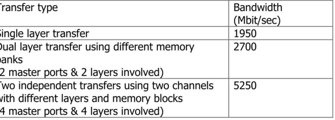
Transfer type Bandwidth
(Mbit/sec)
Single layer transfer 1950
Dual layer transfer using different memory banks
(2 master ports & 2 layers involved)
2700
Two independent transfers using two channels with different layers and memory blocks
(4 master ports & 4 layers involved)
5250
The previous table describes the bandwidth achieved by the DW_ahb_dmac, with a reference speed of 200MHZ, single block transfers of 1KB (256 words) between memory addresses, no other master device accessing the bus.
2.1.4 Interrupt Controller
The inclusion of an interrupt controller appears mandatory in the MORPHEUS architecture. On one hand, the flexibility offered by the ARM9 core in the interrupt handling is limited to two interrupt pins, one fast and one slow interrupt request. On the other hand, the MORPHEUS programming pattern relies a lot on interrupt handling for the synchronization of “microcoded” instructions, that is data chunk/stream transfers (macro-operands handling) and operation on HREs (macro-operations triggering).
The evaluations performed above on the convenience of utilizing pre-verified IP components are very much applicable also to the Interrupt controller selection. As part of the MORPHEUS reference architecture, it is made available the PrimeCell Vectored Interrupt Controller (PL190) by ARM.
As it is the case for the PL175 PrimeCell described in Section 2.1.3, this block is developed and distributed by ARM Ltd and it is especially designed to work with the ARM processor. Moreover, it is distributed as a pre-verified block for inclusion in SoC design. Moreover, PL190 has been used in many commercial products to support ARM-based real time operating systems.
The most relevant features of the PL190 are:
• Compliant to the AMBA bus protocol specification
• Control and status registers mapped on AHB for fast interrupt response
• Support for 32 standard interrupts, 16 vectored IRQ interrupts • Hardware interrupt priority