DOI 10.1393/ncc/i2020-20112-6
Communications: SIF Congress 2019
Proton-induced straining of two-dimensional crystals
E. Blundo(∗)
Physics Department, Sapienza University of Rome - Rome, Italy received 31 January 2020
Summary. — Transition-metal dichalcogenides are an emergent class of semicon-ducting materials with extraordinary opto-electronic properties when reduced to few layers. In the monolayer limit, they emit light efficiently in the visible/infrared re-gion and their flexibility and robustness allow to exploit mechanical deformations to change their inherent properties. Here, we discuss the effect of proton irradiation of bulk WS2, WSe2, WTe2, MoS2, MoSe2and MoTe2 crystals with low-energy beams.
Protons penetrate through the crystal top layer and molecular hydrogen forms. The trapped gas coalesces to create micro-/nano-domes, leading to the blistering of one-layer-thick domes filled with highly pressurised hydrogen, that locally turns the dark bulk material into an efficient light emitter. These domes are robust and stable, and host strong, non-trivial strain fields that cause unprecedented major changes in the band structure of the material.
1. – Introduction
The interest of fundamental and applied sciences for two-dimensional (2D) materials —such as graphene, hexagonal boron nitride (h-BN) and transition-metal dichalcogenides (TMDs)— grounds on the wealth of unusual and alluring electronic, optical, transport and magnetic properties these materials exhibit. Indeed, unique phenomena arise at the few-atom thick limit, stemming from the lowered dielectric screening and the en-hanced quantum effects [1]. The possibility to isolate single layers of these crystals lies in the weak van der Waals (vdW) forces that bind the different layers together. Among vdW materials, TMDs have chemical formula MX2(where M is a transition-metal atom,
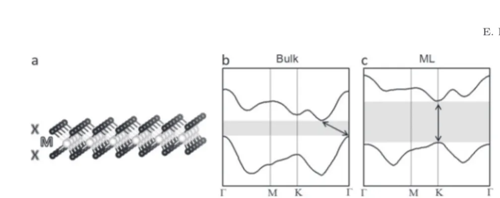
and X is a chalcogen atom) and the crystal structure of a single layer of these mate-rials can be seen in fig. 1(a). In the bulk form, TMDs are typically semiconductors characterised by an indirect gap, as shown in fig. 1(b); when the number of layers is reduced, the gap increases and remains indirect until 2 layers; when the single layer is isolated, the gap becomes direct, involving the K points in both valence and conduction band (see fig. 1(c)) [2]. This peculiar transformation of their electronic properties al-lows monolayer-TMDs to emit light efficiently in the visible or near-infrared range. This
(∗) E-mail: [email protected]
Fig. 1. – (a) Crystal structure of a single layer of a TMD crystal, having chemical formula MX2.
The lattice parameters were taken from refs. [3, 4]. (b), (c) Comparative sketches of typical energy vs. crystal momentum behaviours of (b) bulk and (c) monolayer (ML) TMDs. The shaded areas indicate the band gap, which is larger in the ML with respect to the bulk. The arrows highlight that the gap is indirect in the bulk crystal, while it becomes direct (involving the K point of both valence and conduction band) in the ML.
property, together with a strong spin-orbit coupling [5], makes these materials of great interest for optoelectronics, valleytronics and spintronics. TMD monolayers (MLs) are also important for their catalytic role in the cost-effective production of hydrogen [6]. Finally, few-layer TMDs can withstand surprisingly large mechanical deformations [7], that allow to modify their opto-electronic and transport properties. More specifically, tensile strain leads to a sizeable reduction and modification of the band gap and modifies the absorption and emission properties of the material and the carriers’ mobility and lifetime [8-18]. Periodic strain modulations could also result in pseudo-gauge fields [19], which would enable the observation of non-dissipative topological transport. These ex-amples share the need to achieve spatial control of the mechanical deformations over nanometric/micrometric regions. Several methods exist nowadays to deform 2D mem-branes, among which the formation of bubbles or bulges holds particular relevance since it permits to achieve relatively high strains. Bubbles can be created via the deposition of 2D materials on a substrate, their formation being induced by contaminants (typi-cally hydrocarbons) being trapped during the transfer process [20]. Bulges can instead be obtained by deposition of 2D crystals on pre-designed cavities, that are filled with gases and then pressurised thus causing the 2D membrane to deflect [21]. However, these methods are characterised by some minuses, since the position and size of the bubbles cannot be controlled, while the durability of the bulges is limited to few weeks due to deflating processes.
Here, we discuss a method to create strained TMD-MLs based on the effects of low-energy proton irradiation on the structural and electronic properties of bulk WS2, WSe2,
WTe2, MoS2, MoSe2 and MoTe2. Suitable irradiation conditions lead to the production
of molecular hydrogen just beneath the first X-M-X layer of the bulk crystals. Therein, a spatially localized, partial exfoliation of the material takes place and spherical domes come out on the sample surface [17]. The domes are efficient light emitters, and structural and optical characterizations demonstrate that they have thickness mainly of just one layer, and are filled with H2 gas at pressures ranging from about 10 atm to hundreds of
atms depending on their size, without showing sizable gas leakage [17]. Complex strain fields, evaluated by a mechanical model, modify profoundly the electronic band structure of the curved X-M-X planes [18]. Finally, by lithographically controlling the area of the sample basal plane participating in the hydrogen production process, the domes can be created with the desired density, well-ordered positions and size tuneable from the nanometer to the micrometer scale [17, 22].
2. – Creation of light-emitting micro-/nano-domes
Bulk flakes of WS2, WSe2, WTe2, MoS2, MoSe2 and MoTe2 crystals are exfoliated
with the scotch tape method and deposited on silicon substrates (either bare Si or Si with an Au film or with a SiO2capping). The flakes are identified by optical microscopy
or atomic force microscopy (AFM) measurements, and their thickness ranges between tens and hundreds of layers. The samples are then mounted into a vacuum chamber (evacuated at pressures p < 1.0· 10−6mbar) and irradiated with ionised hydrogen (or deuterium) via a Kaufman source, as described in refs. [17,23]. The samples are typically irradiated with doses in the range 1016–1017ions/cm2. The duration of the whole process
is of the order of few hours.
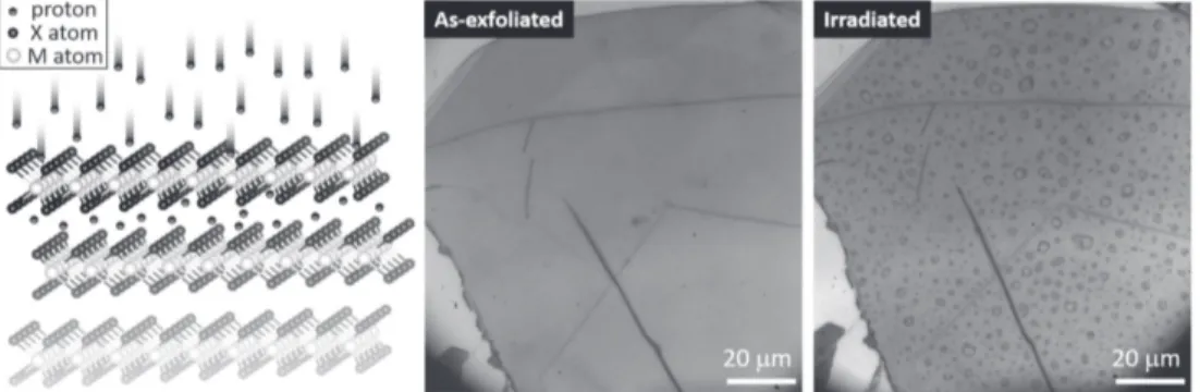
A sketch of the process can be seen in fig. 2(left), while an optical image of a flake be-fore and after proton irradiation can be seen in figs. 2(centre)-(right). Indeed, the surface of the irradiated flake is characterised by the presence of circular features, which were not present before irradiation. Atomic force microscopy measurements of the irradiated flakes reveal that all the compounds are characterised by the presence of dome-shaped bulges, protruding from the irradiated crystal surface, as shown in fig. 3. The size of the domes can be varied by acting on the proton dose and irradiation temperature, as we will discuss later. However, as shown in fig. 4(a), the domes feature a universal height-to-radius ratio, which is independent of their size. This ratio is characteristic of each compound [17, 20], as displayed in fig. 4(b).
Clues on the internal make-up of the domes can be derived by following their low temperature evolution. Figure 5(a) shows the optical microscope images of a bulk WS2
sample irradiated with dose dH = 9.0· 1016ions/cm2. The four images were acquired
at different temperatures. At 290 K, many domes —featuring iridescence— are visible. Their size decreases while cooling down the sample and at low T (see, e.g., the image at 9 K) the domes disappear, and the sample surface looks conspicuously flat. When the temperature is increased/decreased at about 30 K, the domes reappear/disappear sud-denly; as shown in panel (b) the transition completes in less than 10 mK. The transition temperature value is a number close to the critical temperature of H2(33.18 K) and thus
compatible with the presence of molecular hydrogen inside the domes: When T is suffi-ciently low/high, the hydrogen gas liquefies/boils, and the domes deflate/inflate always
Fig. 2. – Left: sketch of the irradiation process, during which an accelerated proton beam is steered onto thick TMD crystals. Centre: optical image (acquired with a 50× objective with NA = 0.5) of a bulk WS2 flake before irradiation. Right: optical image of the same flake after
Fig. 3. – 3D atomic force microscopy (AFM) images of 5 μm×5 μm areas acquired on 6 different TMDs showing the formation of domes in all the samples. The maximum height reached by the domes is also written for each panel.
in the same position. To have further confirmation of this hypothesis, we recorded the transition temperature of more than 500 WS2 domes formed by proton irradiation. To
do that, movies were acquired while warming up the samples from 5 K to ∼50 K, at a low rate equal to ∼40 mK/s. A 50× objective with numerical aperture NA = 0.5 was focused onto the sample, and the image was monitored on a CCD camera to record in real time the sample image with a rate of 10 frames per second. A histogram of the transition temperatures is shown in fig. 5(c). A Gaussian fit (black dashed line) to the histogram (grey bars) —or equivalently a sigmoidal fit to the cumulative function (black point line)— gives an average transition temperature TLVH equal to (32.2± 2.4) K, which is compatible only with the hydrogen liquid-to-vapour phase transition. The fluctuations observed in the measured temperatures (TH
LV) are chiefly due to the spread in the size (and hence in the internal pressure) of the domes. The presence of molecular hydrogen is further confirmed by isotopic shift experiments, as detailed in ref. [17].
Fig. 4. – (a) Maximum height, hm, vs. footprint radius, R, measured by AFM for hundreds
of domes. The data follow a linear behaviour, accounting for a universal height-to-radius ratio independently of R. The data shown here were reproduced with permission from ref. [17]. (b) Average value of the universal ratio for each compound.
Fig. 5. – (a) Optical images of the same area of an irradiated WS2flake at different temperatures.
(b) Optical images of a dome while being deflated (upper panel) and inflated (lower panel), acquired while increasing the temperature. The two images were taken within 10 mK. The black arrows highlight the position of the dome. (c) Histogram of the transition temperature at which the domes appear (left axis). The dashed line is a Gaussian fit to the data. The black point line is the cumulative function of the histogram (right axis). The Gaussian fit to the histogram (or, equivalently, a fit to the cumulative function) provides the average transition temperature TH
LV of proton-irradiated flakes. The data of panel (c) were reproduced with permission from
ref. [17].
We can therefore hypothesise that, during the irradiation process, accelerated protons penetrate through the top MX2 basal plane, becoming confined in between two X-M-X
layers. Therein, the following reaction takes place: 2H++ 2e−→ H2,
the electrons being supplied from the ground contact. This latter hypothesis is supported by the fact that no domes form if the flakes are deposited on insulating substrates, such as kapton. The subsequent build-up of H2 molecules leads to the local blistering of one
or few X-M-X planes, and eventually to the formation of the domes. The above scenario is supported by theoretical studies, which showed that thermal protons remain trapped in the metal plane of X-M-X layers and do not diffuse, thus favouring the accumulation of H2 molecules in the interlayer regions [24].
The thickness of the domes is indeed dependent on the energy of the proton beam during the irradiation process. By using energies of∼100 eV, domes thick several layers form, as suggested by the absence of photoluminescence (PL) emission, typical of indirect gap semiconductors. Instead, if the energy is brought to values below 30 eV, most of the
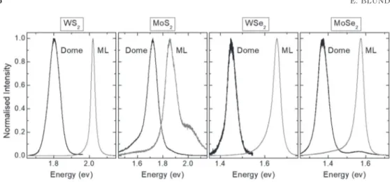
Fig. 6. – Room temperature (T = 290 K) photoluminescence (PL) spectra (black lines) of single domes formed on four MX2compounds; WTe2is a semimetal and thus does not emit a detectable
PL signal, while MoTe2 is subjected to rapid oxidation. The grey lines are the PL spectra of
the corresponding monolayer of the same compound. Each spectrum is separately normalised. The main peak in the spectra corresponds to the direct A exciton (redshifted by the presence of tensile strain [8]), arising from transitions at the K points in the conduction and valence band. The high energy shoulders (especially in Mo compounds) are due to the B exciton transition [25]. For each chemical compound the PL peak energy shift between the dome and the monolayer is equal to about 200 meV, which is attributable to the mechanical stress acting on the domes’ surface. Part of the data was reproduced with permission from ref. [17].
domes emit light efficiently. In fig. 6 we show the PL spectra of some representative domes and of the monolayers of the same compounds at room temperature, corresponding to the free-exciton recombination. The intensity of the PL emission from the domes is typically comparable to that of the monolayers, suggesting a 1-layer thickness for these structures. The energy of the PL peak of the domes is typically∼200 meV lower than that of the MLs, that is ascribable to the strain exerting on the domes surface. Further confirmation of the single-layer nature of the domes is given in ref. [17] i) by second harmonic generation experiments —showing that the domes act as efficient second-generation signal emitters, as typical of TMD MLs; ii) by circular dichroism measurements (the domes feature a degree of circular polarisation ∼60%, similarly to TMD MLs); iii) and by causing the explosion of some domes and measuring their thickness by AFM.
The studies presented so far demonstrate that proton irradiation of bulk TMDs rep-resents an alternative method for the realisation of one-layer-thick, light-emitting, highly deformed TMD domes. A theoretical and optical characterisation of the remarkable deformations achieved with this method will be discussed next.
3. – Characterisation of the strain fields related to the domes
To characterise the mechanical deformation of our 2D TMD membranes and its effect on the opto-electronic properties of these materials, we optimised the proton-irradiation process in order to achieve large domes. This is essential for the optical characterisation of these structures, since any optical setup is diffraction-limited, as detailed in the following. To optimise the parameters, we varied the proton dose and the sample temperature during irradiation. Indeed, for low doses of∼1015ions/cm2we can form only nanometric domes.
Fig. 7. – 3D AFM images of WS2domes created by irradiating the flakes under exactly the same
conditions (dose dH = 8.0· 1016ions/cm2, energy of the proton beam steered onto the sample
equal to 20 eV, same pressure equal to 10−3mbar in the chamber during the process) but for the temperature, which was set at 250◦C (left flake) 150◦C (right flake). Indeed, the size of the domes decreases at higher temperatures.
By increasing the dose, the size of the domes increases, but if the dose is too high the domes start exploding. For our studies, we focused mostly on WS2 and MoS2and found
that the optimum dose is in the range∼5·1016–1·1017ions/cm2. As for the temperature,
we found that for T ∼ 100–150◦C we obtain the largest domes, while their size decreases at higher temperatures, as shown in fig. 7.
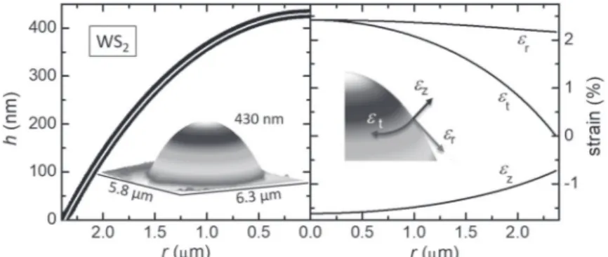
These studies allowed us to create domes with radius R > 2 μm, such as that in fig. 8(a). To quantify the mechanical stress acting on the curved membranes, finite-element methods (FEM) in the framework of the membrane theory can be used, as detailed in refs. [17], [18] and [22]. FEM calculations allow on the one hand to simulate the height profile of the domes, showing an excellent agreement with the experimental profiles measured by AFM (see fig. 8(a)). On the other hand, they allow us to calculate the strain tensor evolution in spherical coordinates, as a function of the distance from the domes’ centre, as shown in fig. 8(b). The calculations show how the strain field related
Fig. 8. – Left: experimental dependence of the dome height h on the distance from the centre r (black points) for a WS2dome. The h-r plot was derived from the AFM image shown as insets.
The white line is the result of finite-element methods (FEM) calculations. Right: dependence of the strain tensor components —in spherical components— on r obtained by FEM calculations for the dome on the left. The definition of the radial (εr) and circumferential (εt) in-plane
components and of the perpendicular (εz) out-of-plane strain component is depicted in the
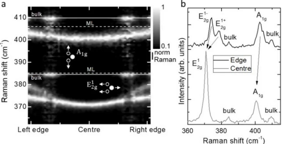
to the domes is isotropic only at the summit, where the two in-plane components (i.e., the radial component, εr, and the tangential component, εt) have the same value. It then becomes strongly anisotropic towards the edges, where the tangential component is null. Analogous behaviours are found independently of the compound, as discussed in refs. [17] and [26]. To support these theoretical calculations, we performed micro-Raman (μ-Raman experiments). These latter were performed in a confocal configuration, by scanning a 532.2 nm laser along a diameter of the domes at steps of about 60 nm. The signal was collected by the same objective employed to focus the laser beam, in a back-scattering geometry. A 100× objective with NA = 0.9 was used, resulting in a Gaussian excitation spot with σ = 230 nm (accounting for the necessity to fabricate relatively large domes). Figure 9(a) depicts a μ-Raman scan across a MoS2 dome (with diameter
D = 3.2 μm), in the region of the out-of-plane (A1g) and of the in-plane (E2g1 ) phonon
modes. The colour plot displays the normalised data in order to follow more clearly the phonon-energy behaviours, showing a progressive softening of both the in-plane and out-of-plane vibrational modes while moving from the edge towards the centre of the dome, in agreement with the expected tensile-strain increase [21]. The intensity of the two modes generally shows some oscillating behaviour which can be ascribed to both
Fig. 9. – (a) One-dimensional, room-temperature (RT), μ-Raman scan along the diameter of a MoS2 dome (with diameter D = 3.2 μm) in the spectral region of the out-of-plane A1g phonon
mode and of the in-plane E1
2g modes (depicted as inset). The horizontal axis indicates the
laser spot position with respect to the dome centre, whereas the vertical axis indicates the Raman shift with respect to the laser line. The Raman data were separately normalised in the two phonon ranges of the in-plane and out-of-plane modes, and the base-10 logarithm of the normalised intensity is shown in a false colour scale (see colour bar). The choice to display the normalised data is aimed at following the phonon-energy behaviours along the scan more clearly. The A1g and E12gmodes of bulk MoS2(at 408.6 cm−1and 383.5 cm−1, respectively, highlighted
by white solid lines) can be noticed (due to the presence of the bulk flake underneath). While the bulk frequencies are constant, the μ-Raman signal of the dome is clearly shifted at lower frequency with respect to the unstrained ML modes (whose frequencies are highlighted by the white dashed lines). (b) Comparison between the μ-Raman spectrum at the edge and at the centre. The effect of strain can be well noticed both in the redshift of the modes and in the splitting of the E12g mode at the edges.
the effect of strain and interferential phenomena, as discussed in ref. [17]. Interestingly, the Raman data of fig. 9(a) and the representative spectra of fig. 9(b) show an evident splitting of the in-plane E1
2g mode towards the edges that is typically induced only by
the presence of anisotropic strains [11, 27], consistently with the theoretical modelling provided by FEM calculations.
To characterise the effects of strain on the opto-electronic properties of TMD MLs, we performed micro-PL (μ-PL) scans, in a configuration analogous to the μ-Raman measurements here discussed. In fig. 10(a) we show the result obtained for a WS2 dome
with radius R = 2.3 μm. While going from the edge towards the summit, both a decrease of the PL signal and a remarkable redshift of the PL peak can be observed. More in detail, the μ-PL spectra recorded close to the edge are dominated by the direct (KCB-KV B) band gap exciton (A), whose energy (equal to 2.00 eV in a strain-free reference WS2
ML [17]) is redshifted by the tensile strain exerted on the dome. As shown in fig. 10(b), as the excitation laser moves toward the centre, the A transition keeps redshifting and concomitantly a new, less intense band, labelled I, takes over and eventually dominates the spectrum. As predicted by numerous theoretical works, the presence of strain in TMD MLs should result in a significant reordering of the energies of the critical points of the band structure [8-16]. In particular, for tensile biaxial strains ε > 1% in WS2 MLs,
the valence band maximum should change from the K to the Γ point of the reciprocal space [8,10-12,14,16], as shown in the sketch of fig. 10(c). We therefore ascribe the I band observed towards the domes’ summit to the indirect KCB-ΓV B transition. Despite the strain values predicted theoretically are affordable, only feeble experimental evidences of this direct-to-indirect transition have been reported so far [28-31]. In the present work, the observation of the indirect band is due to the large tensile strains induced by the pressure exerted on the TMD ML by the H2gas trapped within the dome and favoured
by funnelling phenomena related to the presence of a strain gradient [18]. A confirmation of the indirect nature of the I band is given by the temporal decay of the μ-PL signal of WS2 domes. To perform the measurements, the domes were cooled down at 50 K to
minimize the contribution of non-radiative decay channels [32]. To avoid a reduction of the domes’ size at low temperatures, the domes were capped with a thin methylpentane film, as discussed in ref. [18]. Figure 10(d) shows the μ-PL decay curve relative to the A and I transitions, measured on the very same point of a WS2 dome: The two
transitions exhibit largely different temporal behaviours. The decay time of the A exciton is instrument limited (<250 ps), in agreement with other reports [32, 33]. Instead, the I exciton shows a much longer temporal decay that can be fitted by a double exponential function with two decay times equal to (0.40± 0.06) ns and (2.9 ± 0.7) ns, which clearly points to an indirect optical transition [33]. To determine the strain value at which the direct-to-indirect transition occurs, in fig. 10(e) we show the energy behaviour of the A and I transitions with strain, for the dome shown as inset. The strain was estimated via FEM calculations and the data are plotted as a function of the total in-plane strain εp = εr+ εt, due to the analogous effect of the different in-plane components on the electronic properties of TMDs [8]. The energies of the direct/indirect excitons should vary linearly with strain: EA,I(εp) = EA,I(0)− ΔA,I· p where ΔA,I is the shift rate with strain of the A (I) exciton. To correctly interpret the data in fig. 10(e), however, we have to consider that the strain-induced progressive decrease of the band gap energy from the dome edge towards the centre leads excitons to drift toward the minimum energy available within their diffusion length before recombining [18], that is known as funnel effect. The solid curves displayed in fig. 10(e) result from a fit performed by taking into account the exciton funnelling, while fixing the radius of the collection area Rc to 2.5σ.
Fig. 10. – (a) μ-PL scan at RT along a diameter of a WS2 dome with radius R = 2.3 μm. The
horizontal axis indicates the laser spot position with respect to the dome centre, and the vertical axis indicates the emitted photon energy. The base-10 logarithm of the micro-PL intensity is shown in a false colour scale. (b) μ-PL spectra acquired at the edge, at the centre, and between the edge and the centre of a WS2 dome with radius R = 2.37 μm. At the edge, the direct A
transition dominates the spectrum; halfway, the I transition can be seen as well; at the centre, the spectrum is dominated by the I band. The spectra are normalised for ease of comparison, the intensity factors are quoted. (c) Sketch of the strain-induced direct-to-indirect band gap crossover occurring due to a reordering of the critical points in valence band. (d) Temporal evolution of the μ-PL signal measured at the centre of a dome at T = 50 K, where both the A and I transitions could be observed. The μ-PL spectrum is shown as inset. The grey-shaded area refers to the exciting laser decay curve and sets the temporal resolution. (e) Dependence of the energy of the A and I exciton transitions on the in-plane strain εpfor a WS2 dome with
radius R = 2.86 μm and maximum height hm = 482 nm. The solid lines (relative to the A/I
exciton) are fits performed while taking funnelling into account [18]. These fits entail linear dependences of the exciton energies on εp, which are displayed as dashed lines; the shaded areas
enveloping each curve account for the uncertainty of our fitting procedure. The data presented in panels (d) and (e) were reproduced from ref. [18].
Fig. 11. – Optical images of ordered arrays of domes obtained by patterning the flakes before proton irradiation. The domes on the left were created in openings with size 7.5 μm, those on the right in openings with size 1 μm.
The actual (i.e., free from the funnel effect), strain dependences are shown as dashed lines. This analysis permits to set the direct-to-indirect band gap crossover point at εp = (2.7± 0.3)%, highlighted by vertical dashed lines in fig. 10(e). The displayed fits yield the values of the shift rates and extrapolation energies shown in the figure, which are in agreement with previous experimental [34, 35] and theoretical works [8, 10, 12, 14-16].
Similar findings were observed also in MoS2 and WSe2, as detailed in ref. [18].
4. – Conclusions
In conclusion, we have discussed how proton irradiation of bulk TMDs deeply affects the morphology of the crystal surface, leading to the formation of spherical micro-/nano-domes. These structures are typically stable [17] and emit visible or near-infrared light efficiently, with important prospects for opto-electronic applications. Furthermore, the domes host high and complex strain fields, that enable the unprecedented clear observa-tion of a strain-induced direct-to-indirect bandgap crossover.
The fundamental and applicative prospects of the domes are further enhanced by the possibility to control their formation process via lithographic approaches, allowing the creation of ordered arrays of domes (see fig. 11) and to enhance their built-in strain up to > 10%, thus leading to controllable, giant and non-uniform strain landscapes at the micro-/nano-scale [22].
∗ ∗ ∗
The author acknowledges her supervisor A. Polimeni and her colleagues D. Tedeschi, M. Felici, G. Pettinari, T. Yildirim and Y. Lu for their precious contribution to the research topic presented in this work.
REFERENCES
[1] Ajayan P., Kim P. and Banerjee K., Phys. Today, 69 (2016) 38. [2] Zhang L. and Zunger A., Nano Lett., 15 (2015) 949.
[3] The Materials Project, https://materialsproject.org/ (2018).
[4] Aly¨or¨uk M. M., Aierken Y., C¸ ak´ır D., Peeters F. M. and Sevik C., J. Phys. Chem. C, 119 (2015) 23231.
[5] Xiao D., Liu G.-B., Feng W., Xu X. and Yao W., Phys. Rev. Lett., 108 (2012) 196802. [6] Voiry D., Yang J. and Chhowalla M., Adv. Mater., 12 (2013) 850.
[7] Bertolazzi S., Brivio J. and Kis A., ACS Nano, 5 (2011) 9703. [8] Johari P. and Shenoy V. B., ACS Nano, 6 (2012) 5449.
[10] Shi H., Pan H., Zhang Y.-W. and Yakobson B. I., Phys. Rev. B, 87 (2013) 155304. [11] Chang C.-H., Fan X., Lin S.-H. and Kuo J.-L., Phys. Rev. B, 88 (2013) 195420. [12] Amin B., Kaloni T. P. and Schwingenschl¨ogl U., RCS Adv., 4 (2014) 34561. [13] Das R., Rakshit B., Debnath S. and Mahadevan P., Phys. Rev. B, 89 (2014) 115201. [14] Ortenzi L., Pietronero L. and Cappelluti E., Phys. Rev. B, 98 (2018) 195313. [15] Wang L., Kutana A. and Yakobson B. I., Ann. Phys., 526 (2014) L7.
[16] Zollner K., Faria Junior P. E. and Fabian J., Phys. Rev. B, 100 (2019) 195126. [17] Tedeschi D., Blundo E., Felici M., Pettinari G., Liu B., Yildrim T., Petroni
E., Zhang C., Zhu Y., Sennato S., Lu Y. and Polimeni A., Adv. Mater., 31 (2019) 1903795.
[18] Blundo E., Felici M., Yildirim T., Pettinari G., Tedeschi D., Miriametro A., Liu B., Ma W., Lu Y.and Polimeni A., Phys. Rev. Res., 2 (2020) 012024.
[19] Ochoa H., Zarzuela R. and Tserkovnyak Y., Phys. Rev. Lett., 118 (2017) 026801. [20] Khestanova E., Guinea F., Fumagalli L., Geim A. and Grigorieva I., Nat.
Commun., 7 (2016) 12587.
[21] Lloyd D., Liu X., Christopher J. W., Cantley L., Wadehra A., Kim B. L., Goldberg B. B., Swan A. K.and Bunch J. S., Nano Lett., 16 (2016) 5836.
[22] Blundo E., Di Giorgio C., Pettinari G., Yildirim T., Felici M., Lu Y., Bobba F. and Polimeni A., Adv. Mater. Interfaces, 7 (2020) 2000621.
[23] Felton J., Blundo E., Ling S., Glover J., Kudrynskyi Z. R., Makarovsky O., Kovalyuk Z. D., Besley E., Walker G., Polimeni A., Patan´e A., Molecules, 25 (2020) 2526.
[24] Seel M. and Pandey R., 2D Mater., 3 (2016) 025004.
[25] Frisenda R., Niu Y., Gant P., Molina-Mendoza A. J., Schmidt R., Bratschitsch R., Liu J., Fu L., Dumcenco D., Kis A., Lara D. P. D. and Castellanos-Gomez A., J. Phys. D: Appl. Phys., 50 (2017) 074002.
[26] Wang P., Gao W., Cao Z., Liechti K. M. and Huang R., J. Appl. Mech., 80 (2013) 040905.
[27] Lee J.-U., Woo S., Park J., Park H. C., Son Y.-W. and Cheong H., Nat. Commun., 8 (2017) 1370.
[28] Chaste J., Missaoui A., Huang S., Henck H., Ben Aziza Z., Ferlazzo L., Naylor C., Balan A., Johnson A. T. C.jr., Braive R. and Ouerghi A., ACS Nano, 12 (2018) 3235.
[29] Wang Y., Cong C., Yang W., Shang J., Peimyoo N., Chen Y., Kang J., Wang J., Huang W.and Yu T., Nano Res., 8 (2015) 2562.
[30] Pet˝o J., Dobrik G., Kukucska G., Vancs´o P., Ko´os A. A., Koltai J., Nemes-Incze P., Hwang C.and Tapaszt´o L., 2D Mater. Appl., 3 (2019) 39.
[31] Ma C., Yan J., Huang Y., Zheng Z. and Yang G., Nanotechnology, 31 (2019) 065204. [32] Robert C., Lagarde D., Cadiz F., Wang G., Lassagne B., Amand T., Balocchi A., Renucci P., Tongay S., Urbaszek B. and Marie X., Phys. Rev. B, 93 (2016) 205423.
[33] Liu H., Wang T., Wang C., Liu D. and Luo J., J. Phys. Chem. C, 123 (2019) 10087. [34] He X., Li H., Zhu Z., Dai Z., Yang Y., Yang P., Zhang Q., Li P., Schwingenschlogl
U.and Zhang X., Appl. Phys. Lett., 109 (2016) 173105.
[35] Frisenda R., Dr¨uppel M., Schmidt R., de Vasconcellos S. M., de Lara D. P., Bratschitsch R., Rohlfing M. and Castellanos-Gomez A., 2D Mater. Appl., 1 (2017) 10.