topological semimetal Cd
3
As
2
Adriano Mosca Conte
1,2,*, Olivia Pulci
2,3,*& Friedhelm Bechstedt
4,*Using ab initio density functional theory the band structure and the dielectric function of a bct Cd3As2 crystal are calculated. We find a Dirac semimetal with two Dirac nodes k± near the Γ point on the tetragonal axis. The bands near the Fermi level exhibit a linear behavior. The resulting Dirac cones are anisotropic and the electron-hole symmetry is destroyed along the tetragonal axis. Along this axis the symmetry-protected band linearity only exists in a small energy interval. The Dirac cones seemingly found by ARPES in a wider energy range are interpreted in terms of pseudo-linear bands. The behavior as 3D graphene-like material is traced back to As p orbital pointing to Cd vacancies, in directions which vary throughout the unit cell. Because of the Dirac nodes the dielectric functions (imaginary part) show a plateau for vanishing frequencies whose finite value is proportional to the Sommerfeld fine structure constant but varies with the light polarization. The consequences of the anisotropy of the Dirac cones are highlighted for the polarization dependence of the infrared optical conductivity.
Topology–dependent electronic properties of solids are subject of considerable current interest1,2. In particular, the appearance of ultrarelativistic particles in Dirac cones opens access to novel physics in topological matter. Topological insulators (TIs) are a new class of such materials3,4. Their surfaces or interfaces as well as edges exhibit topologically protected two-dimensional (2D) or one-dimensional linear bands in their fundamental gap as first demonstrated for heterojunctions of the band-gap-inverted HgTe zinc-blende crystals5,6. Another exotic material class is built by topological semimetals, in particular Weyl semimetals (WSMs)1,2 sometimes, in the three-dimensional (3D) case with higher symmetry, called 3D Dirac semimetals7. Unlike two-dimensional (2D) TIs, which represent a quantum spin Hall phase described by a single topological invariant Z2, a 3D TI is charac-terized by four invariants8. A WSM is characterized by the monopole-antimonopole separations in momentum space2. A WSM is a new topological state of 3D quantum matter with Weyl nodes at the Fermi level in the bulk and Fermi arcs on the surface9. Around Weyl nodes the low-energy physics is given as 3D two-component Weyl fermions10. To get a WSM, either time-reversal (T) or inversion (I) symmetry should be broken. In the case of both T and I symmetries, one expects a 3D Dirac semimetal described as four-component Dirac spinors11 with linear dispersion, which can be considered as two distinct Weyl fermions with opposite chirality. The band touch-ing point is the Dirac point but sometimes still called Weyl point. The presence of Fermi arcs on a surface between two corresponding Weyl points whithin the WSM (or even a Dirac semimetal)9 has been recently predicted the-oretically12,13 and confirmed experimentally by means of angle-resolved photoemission spectroscopy (ARPES) for the compounds Na3Bi and Cd3As214–16. The ultra-high carrier mobility measured for Cd3As217 supports the exist-ence of linear bands and massless Dirac or Weyl fermions. High-quality needle-like or large chunky Cd3As2 crystals can be grown using excess Cd17. Indeed, the existence of stable Cd3As2 solids has been known for years18,19. Of particular interest were their semimetallic character and high electron mobility20. The electronic structure of Cd3As2 has been calculated13 for the primitive tetragonal (pt) polymorph with space group P42/nmc
D
( 415h) and 40 atoms in the primitive unit cell, which should appear at intermediate temperatures (475 °C)18. Calculations have been performed also for the non-centrosymmetric, as well as body-centered tetragonal (bct) structure with I41/cd C( 412v) space group and 80 atoms in the unit cell, proposed for temperatures below 475 °C19.
The basic geometry is given as an anti-fluorite arrangement of the atoms with one fourth Cd site vacancy (see Fig. 1). With the corresponding 10-atom building block the pt and bct structures can be constructed. The pt struc-ture with lattice constants a = 8.95 Å and c = 12.65 Å has As atoms in an fcc array and six Cd ones in fluorite-like
1ISMN, Consiglio Nazionale delle Ricerche, Via Salaria Km 29,300 00015 Monterotondo Stazione (Roma) - Italy. 2Dipartimento di Fisica, Università di Roma ‘Tor Vergata’, Via della Ricerca Scientifica 1, I-00133, Rome, Italy. 3I.N.F.N,
- Sezione di Roma ‘Tor Vergata’, and CNR-ISM, Roma, Italy. 4IFTO, Friedrich-Schiller-Universität and ETSF,
Max-Wien-Platz 1, 07743 Jena, Germany. *These authors contributed equally to this work. Correspondence and requests
for materials should be addressed to A.M.C. (email: [email protected]) received: 25 October 2016
Accepted: 27 February 2017 Published: 06 April 2017
www.nature.com/scientificreports/
positions in a 10-atom subsystem. The bct phase has a larger unit cell with a = 12.67 Å and c = 25.48 Å21 in which the empty cube Cd vertices are ordered in 3D rather than in a 2D array.
A very recent X-ray reinvestigation of the bct polymorph21 found a centrosymmetric rather than a non-centrosymmetric symmetry with a distorted superstructure of the antifluorite type with lattice constants
a = 12.633 Å and c = 25.427 Å and space group I41/acd D( 420h). These findings are important for the topological character of Cd3As2. The presence or absence of inversion symmetry has implications on its band structure. In the non-centrosymmetric case the spin degeneracy of the bands in the vicinity of a Weyl point is lifted and Cd3As2 is an example for a Weyl semimetal13. With inversion symmetry the compound represents a 3D Dirac semimetal with no spin splitting. This makes Cd3As2 a 3D electronic analogue of graphene21. This relationship has however not been proven by an orbital analysis. The appearance of linear bands is claimed to be found in the ARPES meas-urements14–16. Other electronic structure studies, e.g. indirect ones by means of optical spectroscopies, became available just recently22,23.
In this paper we study the influence of the stacking of basic units of Cd3As2 on the electronic structure and optical properties at vanishing frequencies. We investigate the analogy of a Dirac semimetal to graphene. For that purpose, we relate the 3D Dirac cones to the topological 3D arrangements of As p orbitals with varying orientation. We distinguish between the Dirac electrons near the Fermi energy and Kane electrons away from it by about 1 eV. The influence of the character as topological semimetal on the optical properties, especially the optical absorption, is a special topic of the paper. In particular, the influence of linear bands near Dirac points on the frequency dependence of the optical conductivity is discussed. The anisotropy of the Dirac cones governs its polarization dependence.
Results
Cd
3As
2building block: simple cubic substructure.
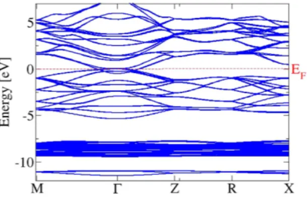
Several basic properties of Cd3As2 polymorphscan be understood within a simplified crystal structure. An fcc sublattice of As atoms with a lattice constant a0 describes the unit cells (see Fig. 1) of such a model crystal. Each As atom is surrounded by 6 Cd atoms at the cor-ners of a cube with an edge a0/2. Two Cd vacancies appear diagonally opposite each other in one face of the small cube. As illustrated in Fig. 1, a distorted anti-fluorite structure with two formula units Cd3As2 and two missing cations appear in a cube of edge length a0. The relaxed Cd positions are described elsewhere21. The resulting lat-tice constant of the cube is a0 = 6.46 Å. It indicates that the bct crystals with space groups I41/cd or I41/acd may be described by non-primitive tetragonal unit cells consisting of 2 × 2 × 4 = 16 cubes with 160 atoms and hence by primitive bct cells with 80 atoms. We study one cube, that is, one building block of the true bct stucture. The studied model crystal with a simple cubic Bravais lattice is a metal, as can be seen in the band structure in Figs 2 and 3. The bands are plotted versus high-symmetry lines in a simple cubic BZ (see ref. 24) because of the sc trans-lational symmetry. The crystal symmetry is however lower. Due to the Cd vacancies the crystal possesses a low symmetry with a point group only with a rotation by 180 degrees around the rotational axis (− 1, 0, 1). The overall band structure in Fig. 2 is rather similar to those of a fluorite crystal, such as CaF2, or anti-fluorite one, such as Na2O. However, there are distinct features in the details.
Despite the overlap around Γ , the bands in Fig. 2 can be arranged in four groups. The conduction bands have a strong Cd5s character in their low-energy parts, as shown in Fig. 3. They are followed by the upper valence bands with strong As4p character. Below (around − 8 eV) one finds Cd4d-derived as well as As4s-dominated bands.
The orbital character of the band states near the Fermi level has been obtained by a Löwdin charge population analysis25 in Fig. 3. In this energy region around Γ the importance of the SOI is clearly visible. Together with the scalar-relativistic effects it tends to bring the Cd s atomic level below the As p one leading to a band inversion Figure 1. Basic geometry of Cd3As2 represented by a 10-atom cube which is a building block for the 80-atom bct structure. It is made of an fcc sublattice of As 80-atoms (green) each surrounded by 6 Cd 80-atoms (purple) disposed at cube vertexes as in an anti-fluorite arrangement but with two Cd vacancies at diagonal corner points of one face of the cube.
between As4p and Cd5s-derived bands at Γ . The situation is similar to the band inversion in the case of the zero-gap semiconductor HgTe crystallizing in zinc-blende geometry26. The fourfold degenerate and, hence, the upper spin-orbit-split As p level pins the Fermi level. However, the lower symmetry of the Cd3As2 model crystal enforces its metallicity. The Cd5s-derived, low-lying parabolic band crossed by the Fermi energy describes a metal. The band inversion due to the scalar relativistic effects already gives a hint for the non-trivial topological character of Cd3As2 similar to the cases of the HgTe and α-Sn26. Another interesting effect of the SOI is the spin splitting of the p-like bands away from Γ in agreement with the fact that the studied system is without inversion symmetry. The band structure in Fig. 3 also shows the absence of linear bands crossing near the Fermi level and, hence, the absence of 3D Dirac cones. This fact already shines light on a possible character of a Weyl or Dirac semimetal in the bct geometries with 80-atom unit cells.
The consequences of the band structure with SOI on optical spectra are illustrated in Fig. 4. The imaginary part of the interband dielectric function (eq. (8) in Method part) in Fig. 4a clearly illustrates the influence of the band structure. At photon energies of ħω ~ 2.6 eV there is a peak mainly due to dipole-allowed optical transitions at the BZ boundary near M points (see Fig. 2). For ω → 0 the imaginary parts show the typical behavior for interband transitions with vanishing gap, while the real parts in Fig. 4b diverge in agreement with the metallic character of the artificial material.
Body Centered Tetragonal Cd
3As
2crystal.
The starting atomic positions in a real bct Cd3As2 crystalhave been determined from those in the artificial sc crystal with cubes of edge length a0 as building blocks. In such a cube four As atoms occupy corner and mid-face positions (0, 0, 0) (0, 1/2, 1/2) (1/2, 0, 1/2) and (1/2, 1/2, 0) of the fcc sublattices. The six Cd atoms surround the As atom in position (0, 0, 0) and sit at the corners of a small cube with edge length a0/2, thereby letting two positions empty to simulate the vacancies. The fcc sublattice of As atoms is then used to build up a non-primitive tetragonal lattice with Bravais vectors (2, 0, 0), (0, 2, 0) and (0, 0, 4) in units of a0. The other Cd atom coordinates are instead found by fixing the center of symmetry in the center of the tetragonal cell and applying the symmetry operations of the I41/acd space group to each of the six Cd atoms surrounding the As atom in (0, 0, 0) position. In this way, all the As atoms are surrounded by six Cd-atom cubes with an arrangement of the vacancies that helix inside the bct unit cell as displayed in Fig. 3 of ref. 21. We test this structure applying symmetry operations of the I41/acd space group (see ref. 27). The resulting structure is indeed centrosymmetric. Finally, the tetragonal crystal with 160 atoms in the non-primitive unit cell is reduced to a bct crystal with 80 atoms in the atomic basis and Bravais lattice vectors (200) (020) and (112) in units of a0. In a final optimization step the atomic positions are allowed to relax until the DFT total energy reaches a minimum. The resulting tetragonal lattice constants amount to c = 25.84 Å and a = 12.93 Å close to the experimental values21. Figure 2. Electronic band structure of the 10-atom substructure of Cd3As2 with SOI in a wide energy range.
The Fermi energy is used as energy zero.
Figure 3. Electronic band structure of the 10-atom substructure of Cd3As2 with (black) and without (dashed red) SOI. The orbital character of the corresponding Bloch states is reported.
www.nature.com/scientificreports/
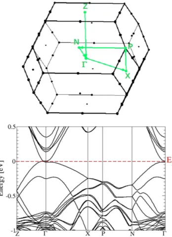
The Cd3As2 band structure calculated with SOI for the relaxed geometry is plotted in Fig. 5 versus high-symmetry lines in the bct BZ. No spin splitting of the bands is visible because of the presence of inversion symmetry. The absolute positions of the band energies, the band dispersions, and the band splittings on the BZ boundary along XP and PN are very similar to those calculated by means of the experimentally determined cen-trosymmetric geometry and an all-electron DFT approach21. All bands are at least twofold degenerate. However, also the non-centrosymmetric bct crystal and a different DFT approach based on projector-augmented waves give very similar results13, because of the rather small spin splittings.
Most interesting is the behavior of the band structure near the Fermi energy EF and the BZ center Γ in Fig. 6. Far away from Γ there are no allowed band states in the low-energy region. Despite the band folding effect due to the larger unit cell, the bands around Γ in Fig. 6 show seemingly some similarities to those in Fig. 3. There are As
p bands crossing the Fermi level. However there are also differences: the Cd s-derived band crossing the Fermi
level in the small cube here disappeared. As more clearly visible in Fig. 7 for an extremely small energy interval, around Γ a small gap of about 0.02 eV is opened. However, along the Γ Z line (and consequently along the oppo-site Γ Z line) twofold degenerate linear bands cross at k±=(0, 0,±k0), thereby forming two fourfold-degenerate
Dirac points at the Fermi level. Therefore the centrosymmetric bct Cd3As2 forms a topological Dirac semimetal with two Dirac points on the tetragonal axis in a distance ± k0 from Γ . Similar to graphene, ideal bct Cd3As2 may be also identified as a multivalley zero-gap semiconductor. In the non-centrosymmetric case13,15 small band split-tings occur and hence Weyl points arise. Around Γ and EF the band structures in Figs 6 and 7 are in agreement with symmetry considerations28. The inverted band structure, already found for the building blocks consisting of two formula units Cd3As2, cannot open up an energy gap due to the C4 rotational symmetry around the tetragonal axis. It protects two 3D Dirac cones touching at two special points k± along the Γ Z line13. Actually, the linearity of the bands at the Dirac points holds just in a very small energy range, as shown in Fig. 6. Therefore, Dirac fermions only appear for excitation energies much lower as claimed discussing ARPES measurements (see discussion below).
The symmetry protection of the vanishing gap at the Dirac nodes even in the presence of SOI is illustrated in Fig. 7 for bands along the tetragonal axis. This figure enlights the SOI influence. Whereas higher-lying conduction bands and lower-lying valence bands are generally shifted toward higher energies, the bands forming the Dirac cones are hardly influenced along the Γ Z direction. The Dirac points are protected by the crystal symmetry (see also arguments in ref. 28). However, also the gap at Γ between the energetically adjacent conduction and valence Figure 4. Imaginary (a) and real (b) part of the dielectric function of the 10-atom substructure of Cd3As2. The components xx, yy, and zz are indicated by red, green, and blue lines, respectively. The Cartesian coordinates are identified with the cubic axes.
bands is also only less shrinked by SOI. The relatively small influence of SOI is in agreement with the above results on the artificial sc Cd3As2 crystal.
The details of the empty (+ ) and filled (− ) band around a Weyl or Dirac point can be described by the hyber-bolic dispersion formula (for a node on the positive Γ Z line)
ε+ −/ ( )k = ±
{
v kF2 2+[vF⊥+ −2/ θ(k⊥−k0)+vF⊥− +2/ θ(k0−k⊥)](k⊥−k0)2}
, (1) 12
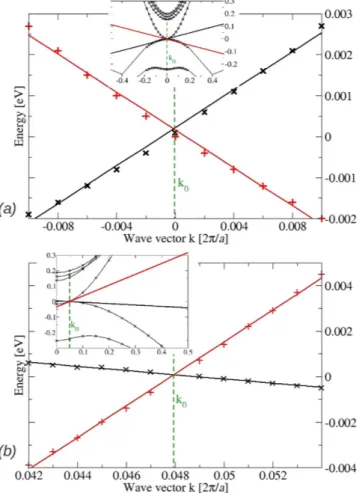
where k‖ lies in the xy plane and k⊥ is along the tetragonal axis z. The corresponding linear fits around k⊥ = k0 and
k‖ = 0 for a small energy interval are depicted in Fig. 8a,b. The three values of the Fermi velocity, resulting in units of 105 m/s are = .v 0 73
F , vF⊥+= .2 2, and vF⊥−= .0 29, indicate the symmetry of the Dirac cones in the xy-plane but
the considerable asymmetry along the tetragonal z axis. The positions of the two Dirac nodes in k space are given by k0 = 0.0481 2π/a = 0.099 Å−1 using the optimized lattice constant a = 12.93 Å. From the insets of Fig. 8 it is Figure 5. Electronic band structure of the bct Cd3As2 superstructure with SOI. (a) bct BZ with indication of
high-symmetry lines and dots. (b) Bands versus high-symmetry lines. The Fermi energy is used as energy zero.
Figure 6. Zoom of the band structure of bct Cd3As2 near one Dirac point on the tetragonal axis ΓZ with SOI.
www.nature.com/scientificreports/
Figure 7. (a) Electronic band structures of bct Cd3As2 along the Γ Z line with (solid black lines) and without SOI (dashed blue lines) (b) Zoom for significantly reduced energies.
Figure 8. Empty and occupied bands (crosses) around the Dirac point =k+
(
0, 0, 0 0481. 2aπ)
at Γ Z versus wavevector k‖ in the xy-plane (a) and k along the z coordinate (b). The linear fits together with the resulting ⊥three Fermi velocities = .vF 0 73, vF⊥+= .2 2, and vF⊥−= .0 29×10 m/s5 to characterize the Dirac cones (1). The
insets display the stronger band dispersion around Dirac node if larger energy and wavevector intervals are studied.
clear that the linearity of the bands at the Fermi level holds just for an extremely small range of energies and just very near the Dirac points.
The computed values differ significantly from the values k0 = 0.032 Å−1 and v
F = 3 × 10⁵ m/s derived for iso-tropic Dirac cones13 or k
0 = 0.12 Å−1, = . − . ×vF 7 6 8 8 10 m/s5 , and vF⊥+= . ×2 3 10 m/s5 29. Optical
measure-ments22 indicate energy-dependent average Fermi velocities which range from 1.2 × 10⁵ to 3 × 10⁵ m/s somewhat larger than our computed values. The comparison with ARPES data15,16,29 is difficult because of the different sur-face orientations, the study of relatively large energy intervals, where the linear bands presented in Fig. 8 change their dispersion into a pseudolinear behavior (see inset), and the necessary refolding of measured bands around the center of the surface BZ to bands around the Dirac points with finite k0 value. Therefore, the Fermi velocities derived from ARPES are hardly compatible with the ones derived from Fig. 8. This especially holds for the meas-urement of occupied linear bands up to 5 eV below the Fermi level29. Correspondingly, the experimentally derived values of 10 × 105 m/s perpendicular to the surface normal and 3.3 × 10⁵ m/s along the normal of the cleavage face are larger than our theoretical ones. The deviations are larger than the 15–20% quasiparticle increases expected from graphene and other honeycomb sheet materials30,31. This is illustrated by the insets in Fig. 8. Away from the Dirac points, the band dispersion and, hence, in the linear approximation, the Fermi energies are larger than the fit values for small energies and wave vectors. According to our findings in Figs 6, 7 and 8, symmetry-protected asymmetric Dirac cones only appear at small electron and hole energies, in contrast to ARPES studies14–16 but in line with results of scanning tunneling spectroscopy (STS)32. The pseudo-linearity observed in ARPES for higher energies may be interpreted in terms of the standard Kane model for semiconductors (see ref. 33), here however for a zero-gap semiconductor23. Especially for surfaces not perpendicular to the tetragonal axis, we expect indi-cations for the band asymmetry when approaching one Dirac node from its left or right side along the Γ Z direc-tion in future high-resoludirec-tion ARPES measurements for extremely low electron energies. The interpretadirec-tion of the current ARPES studies14–16, in which the observed conical feature extending over a wide energy range was identified as symmetry protected Dirac particles, is questionable.
The existence of 3D cones at Dirac nodes k± has been confirmed by other calculations13 and ARPES meas-urements15,16,29. The orbital character of the band states forming Dirac cones above and below the Fermi energy near the Dirac node k± at the Γ Z line is illustrated in Fig. 9. By means of the orbital projection technique we find that all these states around the Dirac nodes possess an As p character. The topological character of the bct Dirac semimetal therefore gives rise to a completely different orbital character of the bands crossing near the Γ point in comparison to that of the artificial sc Cd3As2 crystal. Instead of Cd s here only As p states do contribute. Which p orbital contribute depends, however, on the direction of the k vector. This is demonstrated by their wave function squares plotted also in Fig. 9. They indeed indicate the dominance of As p states, mainly those pointed toward Cd vacancies. In contrast to the in-plane honeycomb arrangement of perpendicular C pz orbitals in 2D graphene, in the topological Dirac semimetal Cd3As2 more or less all As atoms contribute. We trace this fact back to the appearance of Cd vacancies in all directions due to their helix arrangements. The orientation of the As p orbitals depends on the k value and on the energy above or below the Fermi energy. Along Γ Z the HOMO and HOMO − 1 states mainly possess pz character, while px/y orbitals form the LUMO and LUMO + 1 states.
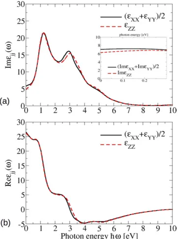
Optical spectra. The optical spectra of bct Cd3As2, which result from the band structure in Fig. 5, are plotted in Fig. 10. More precisely, the real and imaginary parts of the dielectric function are displayed for light polarization Figure 9. Atomic and orbital character of electronic states near a Dirac point. The corresponding
www.nature.com/scientificreports/
parallel and perpendicular to the tetragonal axis. Above ~2 eV they show more or less the same lineshape as the corresponding spectrum for the artificial sc Cd3As2 presented in Fig. 4. The pronounced absorption peak near
ħω = 2.6 eV in Fig. 10a still appears with almost the same intensity. However, the spectra for small photon
ener-gies ħω < 1.5 eV are totally different. The spectral weights are redistributed to guarantee the oscillator strength sum rule. An additional pronounced peak appears at ħω ≈ 1.2 eV, whereas the imaginary parts approach a small positive value for ω → 0. Both observations are consequences of the modified band structure in Fig. 5. The addi-tional peak is due to van Hove singularities in the joint density of states at the lowest optical transition energies near Z and N points. The low-energy behavior is instead dominated by the non-conical 3D Dirac cones. In con-trast to the linear-energy variation of the joint density of states for Dirac cones in 2D graphene-like systems28,34, in the 3D case linear bands give rise to a quadratic energy behavior of the joint density of states. Together with finite optical transition matrix elements in Table 1 and the ω−2 prefactor in expression (8) in the Methods section, finite imaginary parts Im ( )ε ωjj arise in the limit ω → 0.
In order to discuss more quantitatively the low-frequency behavior we first study the optical matrix elements, although only pseudo wave functions are available. Most important is that the momentum matrix elements at the Dirac nodes k = k± are finite in Table 1, despite the vanishing optical transition energy. In the case of 2D graphene we have learnt34 that the matrix element squares averaged over the degenerate states (k ≈ k±)
Figure 10. Real (a) and imaginary (b) part of the dielectric function for the bct phase. Inset: low energy limit for the imaginary part of the dielectric functions, calculated with a more dense k-point grid.
v c j = x j = y j = z HOMO LUMO 5.263 3.224 4.396 HOMO LUMO + 1 7.275 9.314 6.68 HOMO − 1 LUMO 7.275 9.314 6.668 HOMO − 1 LUMO + 1 5.263 3.224 4.396 Tot Σ 25.077 25.077 22.145
Table 1. Optical matrix elements |〈 | | 〉|c p vk j k 2 at a Dirac node k = k
± with a vanishing transition energy
εc,k−εv,k=0 in atomic units 10−2 (ħ/aB)2. Two energetically degenerate valence (conduction) bands
states near the two Dirac points k± contribute. Approximately the direction dependence of the momentum matrix elements is assumed to be equal to the wave vector as known from the Dirac physics for 2D materials31,34. Considering the twofold band degeneracy and the two Dirac nodes in the BZ, it can be analytically shown that for
ω → 0 it holds ε ω = α c v Im ( ) 1 3 , (3) jj Fj
where the Sommerfeld finestructure constant α = e2/ħc and an effective Fermi velocity for the Cartesian direction j = + − −+ + ⊥ − ⊥ + ⊥ − ⊥ + ⊥ − ⊥ v v v v v v v v v 1 2 1 1 5 (4) Fj Fj F F F F F F F 2 2
are applied. In the limit of isotropic Dirac cones and electron-hole symmetry =v vF⊥+=vF⊥−=vFx=vFy=vFz
expression (4) agrees with literature findings22 (apart from a factor 2).
With the values vFx=vFy= .1 24×10 m/s5 and vFz= .1 42×10 m/s5 resulting from eq. 4 with the fit values
in Fig. 8 one obtains the values Imε ωxx( →0)=Imε ωyy( →0)= .5 89 and Imε ω →zz( 0)= .5 14. These
val-ues are in rough agreement with the results of the ab initio calculations performed using eq. 8 and displayed in Fig. 10. The ab initio values Imε ωxx( →0)=Imε ωyy( →0)= .7 0 and Imε ω →zz( 0)= .6 23 are however
somewhat larger indicating smaller effective Fermi velocities, in agreement with the above discussion of linear and pseudolinear bands. The differences between the imaginary parts at zero frequency, characterizing the aniso-tropy of the crystal, 0.75 (analytic formula (3)) and 0.80 (ab initio calculations) are however close to each other. The small deviation is mainly due to the neglect of the k dispersion of the momentum matrix elements (2) away from the Dirac points.
Experimentally the optical reflectivity of [001] and [112]-oriented n-doped Cd3As2 crystals has been studied in a wide frequency range ħω = 0.006–2.8 eV22,23. Using the Kramers-Kronig relation also the real part of the optical conductivity (in cgs units)
σ ω ω π ε ω = Re ( ) Im 4 ( ) (5) jj jj
has been derived. It is isotropic within the (001) plane in agreement with the tetragonal symmetry. Because of relation (5) with (3) we predict for undoped samples
σ ω πα ω ω = c = . v e h v Re ( ) 1 12 6 (6) jj Fj Fj 2
The right-hand side of (6) is by a factor 2 smaller than the derivation in ref. 22 but agrees (apart from ħ2 as a misprint) with theoretical studies for systems with electron-hole symmetry and isotropic Dirac cones35. The reciprocal von Klitzing constant h e/ 2=25 813. kΩ leads to the conductivity in SI units. The linear frequency dependence in (6) also appears in Fig. 11 for small frequencies ħω < 0.4 eV independent of the polarization direc-tion. The absolute conductivity values reasonably agree with the measurements22,23. The slope coefficient
ω σ ω α π = = S d d c v Re ( ) 12 (7) jj jj Fj
with values Sxx = Syy = 0.52 × 10⁻¹⁰ Ω−1 m−1 s and Szz = 0.45 × 10⁻¹⁰ Ω−1 m−1 s computed with the effective Fermi velocities vFj using eq. 4 agree with the ab initio calculations Sxx=Syy= .0 64×10−10Ω−1m s−1 and
Szz = 0.60 × 10⁻¹⁰ Ω−1 m−1 s shown in Fig. 11. The lower slope parameter along the tetragonal axis is in qualitative agreement with recent optical measurements23. Most interesting is the linear behavior of the conductivities in the wide energy interval 0–0.3 eV. This is due to the pseudolinearity of the bands above and below the Dirac points, as discussed above. For very small frequencies (0.0–0.01 eV) a linearity with a different slope is expected, due to the linear bands at the Dirac points (see Fig. 8). To make it visible, one has to sample the BZ around the k± with a
more dense k-point grid. Moreover, the spectrum, in this low energy range, is modified by the Drude term in a real sample. The measured curve for Reσxx(ω) shows an almost linear behavior in the energy range ħω = 0.16– 0.74 eV22 with a slope parameter of about S
www.nature.com/scientificreports/
value 0.64 × 10⁻¹⁰ Ω−1 m−1 s. For small frequencies the experimental spectrum shows several peaks. The power-law fit of the spectra in a wider energy range shows some deviations. The non-linear frequency depend-ence can be traced back to the sublinear k dispersion of the bands away from the Dirac nodes35.
A word of caution is needed, comparing calculated optical spectra with measured ones in the far-infrared region ħω smaller or equal 30 meV. In this spectral region our prediction of a linearly varying frequency depend-ence of the optical conductivity is modified by two effects: (i) Polar optical lattice vibrations will contribute to the optical absorption (see Fig. 1b in ref. 23). (ii) At finite (e.g. room) temperature the occupation of the Dirac cones near the Fermi energy will be slightly modified according to the Fermi function. The resulting free electrons and holes will give rise to Drude terms, which are hardly visible because of their small plasma frequencies. Both effects may slightly influence the limit ω → 0 and hence the slope parameter of the conductivity. Nevertheless,we can state that, despite of the strong anisotropy of the Dirac cones being visible in Fig. 7, the optical conductivity, as an integral quantity, exhibits linear frequency slopes. Those are certaintly dominated by non-conical Dirac fermions. On the other hand, in the higher frequency limit the slopes may be influenced by almost massless Kane-like fer-mions (see discussion in refs 23 and 36). However, the bands in Figs 5 and 7 clearly indicate that the interpretation in terms of massless Kane-like fermions is too simple. The complexity of the band structures around the Dirac points and Γ , in particular in the conduction band region along Γ Z, suggests that for photon energies ħω around 0.5 eV or larger optical transitions, in which no or only one Dirac cone is involved, play a role. The optical spectra ask for a more careful interpretation beyond Dirac fermions or even massless Kane-like fermions.
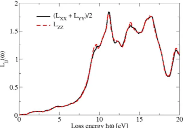
For intermediate energies the fine structure of the energy loss spectra in Fig. 12 is due to the details of the band structure. However, the high-energy behavior of the loss functions is also influenced by collective plasmonic excita-tions of the valence electron with approximate plasma frequencies ωp=(4πe n m2 / )1/2 and corresponding valence electron densities n. According to the band structure in Fig. 2 the valence electrons can be grouped into such due to As p, s and Cd d electrons. Since only the valence s and p electrons can be nearly treated as free electrons in the for-mula for the plasma frequency, two peaks in the loss spectrum near 10.6 eV (only p electrons) and 13.5 eV (s and p electrons) can be explained. Because of the stronger binding, the write effective mass of the Cd d electrons is larger than the free-electron mass. Consequently two other structures near 12.5 and 15.1 eV may be related to collective Figure 11. Real part of the optical conductivity for the bct phase. (a) Black: xx and yy component, (b) red: zz component. The slope parameters Sjj characterizing the constant imaginary parts of the dielectric tensor are also given.
excitations where the d electrons partially contribute. The pronounced peak around ħω = 20 eV can be explained by contributions from the lowest As s and Cd5d bands into higher-lying conduction bands with p character.
Summary and Conclusions
We have studied the most important electronic and optical properties of bct Cd3As2 crystals with 80 atoms in the unit cell by means of the ab initio density functional theory for calculations of the total energy and the electronic structure. The Kohn-Sham eigenvalues and eigenfunctions including the spin-orbit interaction have been used to predict band structures and the independent components of the frequency-dependent dielectric tensor. The results have been compared with recent ARPES and optical reflectivity measurements.
We have demonstrated that important electronic properties are already present in an artificial crystal con-sisting of 10-atom cubes. This holds especially for the tendency of an inverted band structure near the Γ point. However, the topology of the arrangement of the vacancies plays the most important role for the occurrence of Dirac points. In the inversion-symmetric bct geometry with large unit cells Cd3As2 appears as a Dirac semimetal with two Dirac nodes k± at the tetragonal axis near the Γ point. The Fermi energy is pinned at the Dirac nodes, so that the Fermi surface only consists of two separate points. Therefore, bct Cd3As2 may be also interpreted as a multi-valley zero-gap semiconductor as graphene. For small energy variations we indeed found linear bands near k±, which however show a violation of the electron-hole symmetry and a strong asymmetry of the resulting Dirac cones in contrast to 2D graphene. The characteristic three Fermi velocities are of the order of magnitude (but smaller) as derived from ARPES experiments. The linear bands are formed by As p orbitals with varying orientation, underlining the interpretation of bct Cd3As2 as a 3D graphene. We suggest experiments with higher resolution to resolve the strong anisotropy of the Dirac cones along the tetragonal axis for small energies.
Despite the vanishing excitation energy the optical transition matrix elements at k± are finite. Together with the band linearity and the vanishing gap we have derived constant but finite imaginary parts of the dielectric tensor. We demonstrate that the low-frequency value is governed by the Sommerfeld finestructure constant and an effective averaged Fermi velocity. We relate the measured dependence of the optical conductivity on the light polarization to the anisotropic Dirac cones for not too large photon energies. For energies in the range of about 0.5 eV the slopes of the optical conductivity are influenced by Kane-like fermions, also with linear band dispersions.
Methods
In order to compute the structural, electronic and optical properties of Cd3As2 we apply the Density Functional Theory (DFT) as implemented in the code Quantum Espresso package37. Exchange and correlation (XC) are treated within the generalized gradient approximation (GGA) of Perdew, Burke and Ernzerhof (PBE)38. The electron-ion interaction is described by ultrasoft pseudopotentials for the s and p electrons but also for the low-lying Cd4d electrons39. Scalar relativistic corrections (mass and Darwin terms) and spin-orbit interaction (SOI) are taken into account. The inclusion of SOI has been done by first solving an all-electron radial Dirac-like Kohn-Sham equation for each atomic species and then taking the two upper components of the Dirac spinor electronic states in order to build the pseudopotential projectors40,41.
The wavefunctions are expanded into plane waves up to an energy cutoff of 80 (70) Ry for small (large) unit cells with 10 (80) atoms. The Brillouin Zone (BZ) is sampled by a uniform grid of 4 × 4 × 4 (2 × 2 × 2) Monkhorst-Pack k-points42 which are displaced in [111] direction by half a grid step. The atomic positions are determined by relaxing the atomic coordinates for given lattice constants until the Hellmann-Feynman forces are smaller than 1 meV/Å. Since quasiparticle corrections to the positions of the band extrema are vanishing24 around the Fermi level we restrict ourselves to the Kohn-Sham eigenvalues of the DFT. On an absolute energy scale there is a tendency for compensation of the blueshift of the spectra due to quasiparticle effects with their redshift due to excitonic effects24, hence they are neglected. Such effects may only slightly increase the wave-vector dispersion. Indeed, in the case of graphene and other 2D honeycomb material the Fermi velocities increase by about 15–20% due to quasiparticle effects30,31.
Figure 12. Energy loss spectra for vanishing momentum transfer but propagation along the Cartesian axes of the Cd3As2 80-atom bct crystal. The different directions are displayed by colored lines.
www.nature.com/scientificreports/
The frequency-dependent dielectric tensor ε ωij( ) is calculated within the independent-particle approach43. The optical absorption is dominated by the imaginary part of its diagonal elements (j = x, y, z)24
∑∑
ε ω π ω ε ε δ ε ε ω = − − |〈 | | 〉| − − Im e m V f f c p vk k ( ) 2 1 [ ( ) ( )] ( ) (8) jj c v c v j c v k k k k k 2 , , , 2 , , with V as the crystal volume. Here only interband transitions between occupied (|vk〉) and empty (|ck〉) Bloch states with ∈k BZ and corresponding eigenvalues εc k, and εv k, are taken into account. Their occupation is described by a smeared Fermi distribution f ε( ). The real part of (8) follows via the Kramers-Kronig relation24. The strength of the optical transitions in (8) is governed by the matrix elements of the jth component of the momen-tum operator p. For the simple cubic geometry we have used a mesh of 30 × 30 × 30 k-points, whereas a mesh of 5 × 5 × 5 k has been used for the bct phase. For the low energy limit of ε ωjj( ) we have used a more dense mesh of k-points around the Dirac nodes. The dielectric function (8) is directly related to the optical conductivity tensor
σˆ(ω) (see eq. 5). Therefore, the imaginary part in (8) not only allows the calculation of the real part via the Kramers-Kronig relation but also real and imaginary parts of the components of the conductivity tensor. In addi-tion, by means of both quantities also the energy loss function Lj= −Im(1/ ( ))ε ωjj for vanishing momentum transfer can be derived.
References
1. Ando, Y. Topological insulator materials. J. Phys. Soc. Jpn. 82, 102001, doi: 10.7566/JPSJ.82.102001 (2013).
2. Hasan, M. Z., Yu, S.-Y. & Biang, G. Topological insulators, topological superconductors and weyl fermion semimetals: discoveries, perspectives and outlooks. Physica Scripta T 164, 014001, doi: 10.1088/0031-8949/T168/1/019501 (2015).
3. Hasan, M. Z. & Kane, C. L. Colloquium: Topological insulators. Rev. Mod. Phys. 82, 3045–3067, doi: 10.1103/RevModPhys.82.3045 (2010).
4. Moore, J. E. The birth of topological insulators. Nature 464, 194–198, doi: 10.1038/nature08916 (2010).
5. Volkov, B. A. & Pankratov, O. A. Two-dimensional massless electrons in an inverted contact. JETP Lett. 42, 178 (1985). 6. Kusmartsev, F. V. & Tsvelik, A. M., Semimetallic properties of a heterojunction. JETP Lett. 42, 259 (1985).
7. Zhu, Z. & Hoffman, J. E. Condensed-matter physics: Catching relativistic electrons. Nature 513, 319–320, doi: 10.1038/513319a (2014).
8. Fu, L. & Kane, C. L. Topological insulators with inversion symmetry. Phys. Rev. B 76, 045302, doi: 10.1103/PhysRevB.76.045302 (2007).
9. Wan, X., Turner, A. M., Vishwanath, A. & Savrasov, S. Y. Topological semimetal and fermi-arc surface states in the electronic structure of pyrochlore iridates. Phys. Rev. B 83, 205101, doi: 10.1103/PhysRevB.83.205101 (2011).
10. Weyl, H. Elektron und gravitation. i. Zeitschrift für Physik 56, 330–352, doi: 10.1007/BF01339504 (1929). 11. Dirac, P. A. M. The quantum theory of the electron. P. Roy. Soc. Lond. A Mat. 117, 610–624 (1928).
12. Wang, Z. et al. Dirac semimetal and topological phase transitions in A3bi (a = Na, k, rb). Phys. Rev. B 85, 195320, doi: 10.1103/
PhysRevB.85.195320 (2012).
13. Wang, Z., Weng, H., Wu, Q., Dai, X. & Fang, Z. Three-dimensional dirac semimetal and quantum transport in cd3as2. Phys. Rev. B
88, 125427, doi: 10.1103/PhysRevB.88.125427 (2013).
14. Liu, Z. K. et al. Discovery of a three-dimensional topological dirac semimetal, na3bi. Science 343, 864–867, doi: 10.1126/ science.1245085 (2014).
15. Neupane, M. et al. Observation of a three-dimensional topological dirac semimetal phase in high-mobility cd3as2. Nat Commun 5, –, doi: 10.1038/ncomms4786 (2014).
16. Borisenko, S. et al. Experimental realization of a three-dimensional dirac semimetal. Phys. Rev. Lett. 113, 027603, doi: 10.1103/ PhysRevLett.113.027603 (2014).
17. Liang, T. et al. Ultrahigh mobility and giant magnetoresistance in the dirac semimetal cd3as2. Nat Mater 14, 280–284, doi: 10.1038/ nmat4143 (2015).
18. Stackelberg, M. & Paulu, R. Untersuchungen an den Phosphiden und Arseniden des Zinks und Cadmiums. Das Zn3P2-Gitter Z.
Phys. Chem. B 28, 427 (1935).
19. Steigmann, G. A. & Goodyear, J. The crystal structure of cd3as2. Acta Crystallographica Section B 24, 1062–1067, doi: 10.1107/ S0567740868003705 (1968).
20. Rosenberg, A. J. & Harman, T. C. Cd3as2 – a noncubic semiconductor with unusually high electron mobility. Journal of Applied
Physics 30, 1621–1622, doi: 10.1063/1.1735019 (1959).
21. Ali, M. N. et al. The crystal and electronic structures of cd3as2, the three-dimensional electronic analogue of graphene. Inorg. Chem.
53, 4062–4067, doi: 10.1021/ic403163d (2014).
22. Neubauer, D. et al. Interband optical conductivity of the [001]-oriented dirac semimetal cd3as2. Phys. Rev. B 93, 121202, doi:
10.1103/PhysRevB.93.121202 (2016).
23. Akrap, A. et al. Magneto-Optical Signature of Massless Kane Electrons in Cd3As2. Phys. Rev. Lett. 117, 136401, doi: 10.1103/
PhysRevLett.117.136401 (2016).
24. Bechstedt, F. Many-Body Approach to Electronic Excitations: Concepts and Applications (Springer-Verlag, Heidelberg, 2015). 25. Vitali, L. et al. Electronic Structure of Surface-supported Bis(phthalocyaninato) terbium(III) Single Molecular Magnets. Nano Lett.
8, 3364, doi: 10.1021/nl801869b (2008).
26. Küfner, S. & Bechstedt, F. Topological states in α − Sn and hgte quantum wells: A comparison of ab initio results. Phys. Rev. B 91, 035311, doi: 10.1103/PhysRevB.91.035311 (2015).
27. http://img.chem.ucl.ac.uk/sgp/large/142a.htm.
28. Young, S. M. et al. Dirac semimetal in three dimensions. Phys. Rev. Lett. 108, 140405, doi: 10.1103/PhysRevLett.108.140405 (2012). 29. Liu, Z. K. et al. A stable three-dimensional topological dirac semimetal cd3as2. Nat Mater 13, 677–681, doi: http://dx.doi.
org/10.1038/nmat3990 (2014).
30. Yang, L., Deslippe, J., Park, C.-H., Cohen, M. L. & Louie, S. G. Excitonic effects on the optical response of graphene and bilayer graphene. Phys. Rev. Lett. 103, 186802, doi: 10.1103/PhysRevLett.103.186802 (2009).
31. Matthes, L., Pulci, O. & Bechstedt, F. Massive dirac quasiparticles in the optical absorbance of graphene, silicene, germanene, and tinene. Journal of Physics: Condensed Matter 25, 395305 (2013).
32. Jeon, S. et al. Landau quantization and quasiparticle interference in the three-dimensional Dirac semimetal Cd3As2. Nat. Mater. 13,
851, doi: 10.1038/nmat4023 (2014).
33. Enderlein, R. & Horing, N. J. M. Fundamentals of Semiconductor Physics and Devices (World Scientific, 1997).
34. Matthes, L., Gori, P., Pulci, O. & Bechstedt, F. Universal infrared absorbance of two-dimensional honeycomb group-iv crystals. Phys.
42. Monkhorst, H. J. & Pack, J. D. Special points for brillouin-zone integrations. Phys. Rev. B 13, 5188–5192, doi: 10.1103/PhysRevB.13.5188 (1976).
43. Adolph, B., Gavrilenko, V. I., Tenelsen, K., Bechstedt, F. & Del Sole, R. Nonlocality and many-body effects in the optical properties of semiconductors. Phys. Rev. B 53, 9797–9808, doi: 10.1103/PhysRevB.53.9797 (1996).
Acknowledgements
O.P. acknowledges financial support from EU HORIZON2020 RISE project CoExAN (GA644076). CPU time was granted by CINECA.
Author Contributions
F.B. conceived the project, A.M.C. and O.P. did the calculations, all authors analysed the results. All authors reviewed the manuscript.
Additional Information
Competing Interests: The authors declare no competing financial interests.
How to cite this article: Conte, A. M. et al. Electronic and optical properties of topological semimetal Cd3As2.
Sci. Rep. 7, 45500; doi: 10.1038/srep45500 (2017).
Publisher's note: Springer Nature remains neutral with regard to jurisdictional claims in published maps and institutional affiliations.
This work is licensed under a Creative Commons Attribution 4.0 International License. The images or other third party material in this article are included in the article’s Creative Commons license, unless indicated otherwise in the credit line; if the material is not included under the Creative Commons license, users will need to obtain permission from the license holder to reproduce the material. To view a copy of this license, visit http://creativecommons.org/licenses/by/4.0/