Università degli Studi di Ferrara
DOTTORATO DI RICERCA IN
Fisica
CICLO XXI
COORDINATORE Prof. Filippo Frontera
Surface interaction mechanisms in metal-oxide
semiconductors for alkane detection
Settore Scientifico Disciplinare FIS/01
Dottorando Tutore
Contents
Introduction v
1 Metal-oxide semiconductors: electronic behaviour and working
mecha-nism 1
1.1 Bulk and band model . . . 2
1.2 Intrinsic surface states . . . 4
1.2.1 Double layer . . . 4
1.2.2 The equation of Poisson . . . 6
1.2.3 Spherical model and limits to the depletion approximation . . . 10
1.3 Working mechanism models . . . 15
1.3.1 Conductance variation . . . 15
1.3.2 Conduction and morphology of the sensitive layer . . . 17
1.3.3 Effects of adsorbed gases on electric resistance of sensors . . . 21
2 Gas adsorption processes 27 2.1 Physisorption and chemisorption . . . 27
2.2 Adsorption isotherms . . . 30
2.2.1 The Langmuir isotherm . . . 30
2.2.2 The BET isotherm . . . 33
2.2.3 The Freundlich isotherm . . . 34
2.3 The rates of surface processes . . . 35 3 Synthesis and deposition techniques 39
CONTENTS 3.1 Synthesis of the nanostructured metal-oxide
powders . . . 39
3.2 The serigraphic process . . . 40
3.3 Production process of thick films . . . 41
3.3.1 Preparation of the pastes . . . 43
3.3.2 Substrates . . . 44
3.3.3 Printing . . . 45
3.3.4 Drying up . . . 46
3.3.5 Sinterisation . . . 46
4 Temperature-programmed desorption measurements 49 4.1 Theoretical model . . . 50
4.2 TPD and ITPD experiment . . . 52
4.2.1 Experimental apparatus . . . 53
4.2.2 Description of the experiments . . . 54
4.3 Results and discussion . . . 54
5 Alkane sensing 63 5.1 Alkane oxidation via heterogeneous catalysis . . . 63
5.2 Conduction measurements . . . 65
5.2.1 Experimental conditions . . . 65
5.2.2 Results and discussion . . . 68
Conclusions 87
Introduction
Solid state gas sensors represent a remarkable application of modern nanotechnologies and complex physico-chemical processes. These devices transduce a chemical quantity, such as a gas concentration, into an electric signal.
Gas sensors based on semiconductive materials have gained an increasing interest, thanks to their advantageous characteristics in comparison with traditional systems (based on optics and spectroscopic analysis), which are more cumbersome, expensive and require a careful maintenance by qualified personnel. On the other hand, solid state devices are characterised by small encumbrance, easy usage, low-cost, reliability, high sensitivity and repeatability. However, sensor electric properties are also influenced by the interaction with molecules of gases present in the atmosphere other than the target gas. It is difficult to eliminate the effect of interfering gases, whose signal may overcome that of the gas of interest. This intrinsic lack of selectivity made research in this field to come to a standstill and hindered a significant development of such sensors. Additivation of sensitive material by means of catalysts (such as Pd, Pt and Au) seems to be a viable way to promote or hin-der a chemical reaction instead of another. Nonetheless, experiments have not solved this problem yet. Another solution is the usage of filtres, though the number of experimental studies in this direction is meagre.
Semiconductor gas sensors are mainly applied to environmental monitoring, in order to keep pollutant gas concentrations under control, because of their negative effects on human health and on monuments. Also indoor applications are very useful, e.g. for the detection of gas leaks from both heating system and gas kitchen. For these reasons, researchers have concentrated their studies towards gases like CO, CO2, NOx and alkanes.
Light alkanes have been widely studied for many years especially in catalysis. Their behaviour is relatively easy to understand because of their simple molecules. Therefore,
Introduction a great number of publications appears in literature with theories and results concerning alkane reaction mechanisms. Moreover, these gases are very interesting also for gas sensing. Methane and propane have been extensively used for combustion, propane is employed for the production of hydrogen by steam-reforming plants, and i-butane is recognised to be very useful in charge particle detection in nuclear physics.
A clearer analysis of surface reaction phenomena is the key to find a solution to the problem of limited selectivity. This approach has been applied to gases of great interest, such as alkanes. The main aim of this dissertation is to clarify some theoretical and exper-imental aspects related to the sensing processes of metal-oxide semiconductors, studying their surface and conduction properties.
The first chapter deal with the electronic behaviour and the conduction mechanism of metal oxides, whereas the second contains a general view of gas adsorption processes. The synthesis and the deposition methods, employed for the production of the sensitive powders and of the thick film sensors, are described in chapter 3. The subsequent chapters are dedicated to the experimental measurements. First, surface interactions between metal-oxide powders and oxygen were analysed by means of temperature-programmed desorption techniques. The results of desorption experiments, performed at the IRCELYON (Institut de Recherches sur la Catalyse et l’Environnement de Lyon), are presented and discussed in chapter 4. In the end, sensing of light alkanes was studied. Chapter 5 comprises an explanation of the reaction mechanisms between alkanes and the surface of the sensors and the discussion of the results of conduction measurements, carried out at the Sensor and Semiconductor Laboratory of Ferrara.
Chapter 1
Metal-oxide semiconductors:
electronic behaviour and working
mechanism
Metal-oxide semiconductors are widely studied and used as raw materials for chemoresistive gas sensors. These devices are found to be very useful in the detection of toxic and pollutant gases. Indeed, they are recognised to have established advantages such as low cost, compactness and ease of integration with integrated circuit technology.
As Wagner and Hauffe [1] discovered in 1938, adsorbed atoms and molecules on the sur-face of a semiconductor influence its properties, such as conductivity and sursur-face potential. Later, many researchers [2, 3, 4] studied these effects on semiconductor electric conduc-tance. The first applications of these discoveries arrived soon after [5, 6] together with the production of the first chemoresistive-semiconductor-gas sensors. Since that moment, technology development and the problem of toxic and pollutant gas monitoring encouraged improvements in the production and in the performances of different kind of gas sensors.
A large part of commercial gas sensors are built with SnO2, while TiO2 and ZrO2 are
Metal-oxide semiconductors: electronic behaviour and working mechanism
1.1
Bulk and band model
Electrons in a crystal can only adopt energy values which stay inside certain ranges or more specifically bands of energy. Energy bands are separated from prohibited energy bands, called band gap [7]. In a semiconductor the highest energy band occupied by fundamental state electrons is called valence band, while the upper band, in which electrons can be promoted, is called conduction band. Conduction band would be completely empty in a perfect crystal at 0 K. However, we remark that solids have an imperfect structure, as a consequence electrons are present in the conduction band or miss in the valence one. Therefore, semiconductors applied on gas sensing are based on the fact that electrons could be transferred or removed from the conduction band, in order to induce consistent variations in the conductivity of the material.
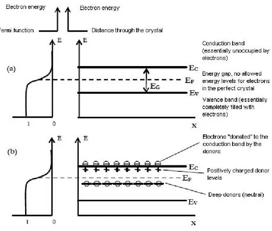
Semiconductor band model is depicted in Fig. 1.1, where electron energy is on the x-axis, while the distance inside the crystal is on the y-axis. The energy gap Eg
repre-sents the demanded energy for valence electron excitation (promotion to conduction band). Electron distribution in the different energy levels under thermal equilibrium condition is given by the function of Fermi f :
f = 1 1 + eE−EFkT
(1.1) Where k is the Boltzmann constant and T is the absolute value of temperature. This function expresses the probability that an energy level E is occupied by an electron. The energy of Fermi is that value of energy EF where f=1/2, that is to say that an energy level
Figure 1.1: Fermi function and band diagram for semiconductors; (a) intrinsic semiconductor; (b) n-type semiconductor with deep and shallow donors.
Metal-oxide semiconductors: electronic behaviour and working mechanism the electron density, n, can be written (employing Boltzmann approximation, for which f is reduced to a simple exponential, if E-EF " kT) [7]:
n = NC · e−(EC−EF)/kT (1.2)
where NC is the effective density of the states next to the bottom of the conduction band.
1.2
Intrinsic surface states
A sudden interruption of the crystal lattice periodicity occurs on the surface. Thus, surface atoms or ions have an incomplete coordination number (number of first neighbours), which causes a rearrangement and a greater reactivity in comparison to that of bulk atoms or ions. The perturbation of lattice periodicity is enough to create intrinsic localised electronic states at surface level [9].
In ionic materials, as many metal oxide semiconductors are, every surface ion, having incomplete coordination, is even not coupled with the opposite charge ion. In a metal oxide, metal cations tend to catch electrons behaving as acceptors, while oxygen anions tend to release electrons behaving as donors. In this last case, one can visualise the electron as not coupled in an orbital, which extends up till outside the surface. Now, it is ostensible that this electron could both accept another electron to create a couple and enter in the bulk, leaving a unoccupied surface state.
In the end, it is possible to say that both energy levels, acceptors and donors, are present on the surface of the crystal. Fig. 1.2 shows a band model which includes the surface of the crystal and indicates the presence of surface states [7]. The case when there is no net charge is used for simplicity. This is the so-called flat-band case. As one can
Figure 1.2: Surface states bands at the n-semiconductor surface. In the diagram, the surface states are assumed to be neutral (acceptor states are unoccupied and donor states are occupied). For simplicity in many arguments, the bands of surface states can be represented as single energy levels.
Metal-oxide semiconductors: electronic behaviour and working mechanism they will move from the conduction band to those lower-energy states, forced by this new energetically more favourable configuration. With the upper levels (acceptors) completely empty and the lower levels (donors) completely full, by definition the Fermi energy must be in between. Therefore, the electrochemical potential of the electrons at the surface states is lower than that in the conduction band. Thereby, electrons will have to move towards the surface states. When such transitions occur, a charge builds up at the surface and a countercharge in the bulk (the countercharge being that of the donor ions).
Fig. 1.3 shows an n-type semiconductor after the charge has moved from the donor ions to the surface states. A double layer is formed, with the positively charged donors in the semiconductor as space-charge layer on the one side, and the negatively charged surface states as a sheet of charges on the other side. Thus, an electric field develops between these two charge layers. The term space-charge layer refers to the region, where the uncompensated donor ions are the only important charged species. The charge density from such ions is Ni=ND-NA, where ND is the donor density and NAis the acceptor density.
The term depletion layer is used to describe this region, because all the mobile carriers (in figure 1.3, the electrons) have been exhausted from the region and moved to the surface [7].
A scheme of two grains of metal-oxide powder is depicted in Fig. 1.4, where the space-charge region around the surface and at the contact point is shown. The oxygen species adsorbed create the surface-charge layer, which is responsible for the intergranular potential barrier that conduction electrons have to overcome, in order to go from a grain to another.
1.2.2
The equation of Poisson
Figure 1.3: Double layer. Electrons from the conduction band are captured by surface states, leading to a negatively charged surface with the counter-charge the positively charged donors near the surface.
dent of x (the distance into the crystal), in general, because the donors or acceptors have been introduced into the material in such a way as to make them independent of distance (homogeneous doping). A change in coordinates is helpful in relating the mathematics to the band diagram, where, rather than potential, the energy of an electron is plotted. We define to that end the parameter V as:
V (x) = Φb − Φ(x) (1.4)
where Φb is the potential in the bulk of the semiconductor. Then the first integration of
Poisson’s equation is straightforward: dV
dx =
qNi(x− x0)
!!0
(1.5) where x0 is the thickness of the space-charge region. The thickness of the space-charge
Metal-oxide semiconductors: electronic behaviour and working mechanism
x≥ x0 the semiconductor is uncharged, so we use the boundary condition that dV/dx=0
at x=x0. For n-type material NDx0(=Nix0) is the number of electrons (per unit area)
extracted from the surface region of thickness x0, and this equals the number of electrons
(per unit area) moved to the surface:
Nix0 = Ns (1.6)
where Ns is the density of charged surface states. The integration of 1.5 leads to:
V = qNi(x− x0)
2
2!!0
(1.7) because V was defined zero at x=x0. This leads to the relation of Schottky; the value of
the surface barrier Vs (V at x=0) is
Vs=
qNix20
2!!0
(1.8) The energy qVsis the energy that electrons must attain before they can move to surface
energy levels. In the end, using 1.6 to eliminate x0 from 1.8, the following expression is
obtained: Vs = qN2 s 2!!0Ni (1.9) an important relation describing the potential difference between the surface and the bulk (or, as qVs, the energy difference of electrons between the surface and the bulk) as a
function of the amount of charge Ns on the surface. In the above calculus, the charge was
assumed to be on clean surface, but equally well the charge can be associated, for example, to the density of negatively charged adsorbed oxygen (e.g., O−2), of critical interest for semiconductor gas sensors operating in air.
Metal-oxide semiconductors: electronic behaviour and working mechanism
1.2.3
Spherical model and limits to the depletion approximation
The barrier of Schottky is usually studied within the depletion approximation in plane geometry. However, when considering a grain with radius R comparable to the dimension of the depletion region, the curvature effects become relevant and some modifications are necessary [10].
First of all, the equation of Poisson is solved in spherical symmetry: 1 r d2 dr2[rΦ(r)] =− qNd ! (1.10)
where Nd is the density of donors, which are supposed to be completely ionised at the
working temperature. R is defined as the radius of the grain, while R0 the radius of the
neutral region (see Fig. 1.5). When considering the depletion approximation, the density of charge is qNd in the whole region thick R-R0 (x0 in par. 1.2.2) and zero elsewhere.
Moreover, another hypothesis is that Φr becomes zero for r=R0, that is to say that the
electric field -∇Φ(r) is zero for r≤R0. It has to be remarked that in this approximation
R-R0 represents both the thickness of the depletion region and the length of the potential
extinction.
The difference between the potential in the centre of the grain and that on the surface is called the built-in potential V. Therefore, the following initial conditions are imposed to Eq. 1.10:
[Φ(r)]R0 = 0 − ∇Φ(r)|R0 = 0 (1.11)
Figure 1.5: Scheme of a grain, where Ntis the surface density of acceptors and Ndis the density
Metal-oxide semiconductors: electronic behaviour and working mechanism It is worth remarking that the grain must be altogether neutral, so that the surface charge density, qNt, exactly compensates for the space charge in the depleted region. This
implies: Nt= Nd ! R 3 − R3 0 3R2 " (1.13) The spherical model just described is still based on the depletion approximation, which unfortunately fails, when the dimension of the grain goes down a limit value.
When considering an n-type semiconductor, the charge density must be expressed as fol-lows:
ρ(r) = qNd− qNdeqΦ(r)/kT (1.14)
where the second term is the contribution of the mobile charge carrier at nonzero temper-ature.
The charge density used in the depletion approximation must be achievable from Eq. 1.14, in which the zero of energy (and potential) is fixed at ECBB (bulk) (CBB means
conduction band bottom). However, in the case of powdered or polycrystalline semicon-ductors, the bulk can be reached only if the grain is sufficiently large, while the depletion approximation assumes that the zero-potential is always attained, independently of the grain size. Thus, when it is not possible to apply the approximation, we have to solve the following equation in spherical coordinates:
1 r d2 dr2[rΦ(r)] =− qNd ! + qNd ! e qΦ(r)/kT (1.15)
R. Defining this values as -Vs, we set the second boundary condition for Eq. 1.15:
Φ(R) =−Vs (1.16)
However, a difficulty arises, when we want to compare Vswith what can be experimentally
measured. The methods employed commonly to determine the surface potential measure the built-in potential V=Φ(0)-Φ(R) (the difference between the potential at the CBB in the centre, Φ(0), and the potential at the surface, Φ(R)). If R≥ Ξ (where Ξ is the potential extinction length), φ can be considered zero and the measured value V coincides with Vs.
In the case of a small grain, the boundary condition Φ(R)=-V is not correct.
As for the depletion approximation, the neutrality of the grain is imposed. This means that the integral of the charge density in Eq. 1.14 over the entire volume of the grain equals the integration of the surface acceptor state density Nt, which is assumed to be
uniform over the surface: 4π # R 0 $ qNd− qNdeqΦ(r)/kT % r2dr = 4πR2qN t (1.17)
Therefore, the system of equations constituting the model based on the complete charge density is: 1 r d2 dr2[rΦ(r)] =− qNd ! + qNd ! e qΦ(r)/kT, −dΦ(r)dr |r=0 = 0, Φ(r)|r=R=−Vb, −dΦ(r)dr |r=R− = qNt ! (1.18)
The last equation is derived from the neutrality condition of Eq. 1.17. The model is based on six parameters (T, !, Vb, Nd, Nt and R) and one unknown function (Φ(r)). Nd and !
characterise the semiconductor and can be directly measured with T. The value of Vs for
Metal-oxide semiconductors: electronic behaviour and working mechanism
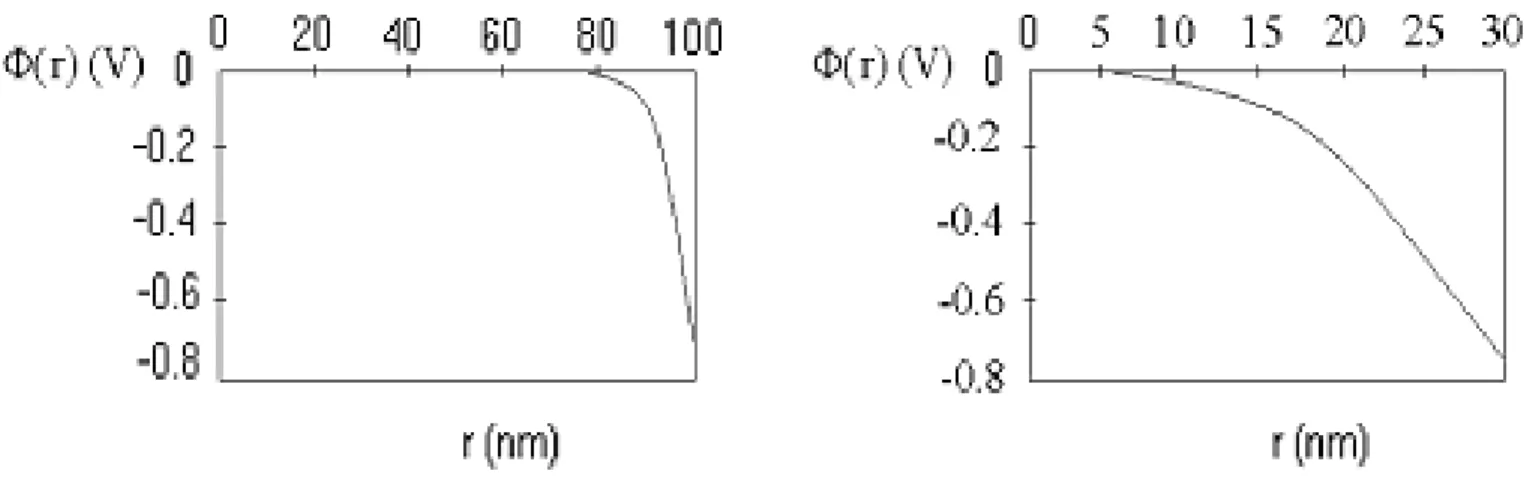
Figure 1.6: Potential shape vs coordinate r for R=100 nm (left) and R=30 nm (right). The potential vanishes at a distance Ξ=22 nm far from the surface in both cases.
can be measured through an Arrhenius plot (a measurement of the conductance under a slow change in sensor temperature). Thus, if the material and the environment are fixed, the potential Φ(r) and the surface-state density Ntcan be determined as a function of the
grain radius R.
The numerical solution of the model is reported, employing the experimental values for SnO2 in air (T=400◦C, !=10−10F/m, Nd=5×1018cm−3 and Vs=0.68V). The Debye
length is λD=2.7nm and the zero value of the potential is reached at a constant distance
Ξ ∼=8λD ∼=22nm from the surface, provided that R> Ξ.
The solution for R=100 nm and R=30 nm is shown in Fig. 1.6, which are typical values of different ranges of approximation: in the first case, R" Ξ " λD, thereby the depletion
Figure 1.7: Potential shape vs coordinate r for R=10 nm. The potential does not vanish even on the centre of the grain.
1.3
Working mechanism models
A chemoresistive sensor is able to respond to an external stimulus (e.g., a gas concentration) with an electric signal (usually, a conductance change). Indeed, when a gas arrives at the surface of a sensor, it interacts both physically and chemically. Adsorption from the gaseous phase leads to charge exchanges between the adsorbate layer and the material itself, meaning a variation of the free electron concentration and, therefore, of the total number of electrons available for conduction. Many researchers have endeavoured to explain the basic mechanism of chemoresistive gas sensors. However, many aspects have not been deeply understood yet. In this section, the main sensing mechanism models will be described.
1.3.1
Conductance variation
Two kind of working processes can be distinguished for chemoresistive sensors [7]: the first one concerns bulk conducibility variations, the second one is connected to surface conducibility variations. Bulk conducibility variations are very important in oxygen par-tial pressure measurements. In this case, bulk chemical defects play a fundamental role, because the bulk has to be in equilibrium with atmospheric oxygen.
Metal-oxide semiconductors: electronic behaviour and working mechanism On the other hand, the second class of sensors is even able to detect different gases from oxygen. Indeed, the equilibrium value of surface conductance, which is reached in conditions of constant oxygen partial pressure, is influenced by the perturbing presence of surrounding gases. This class of sensors is sensitive to the variations of oxygen concentra-tion too, but bulk chemical defects are less important for the measurements of atmospheric gases. The study of this second class of sensors will be mainly deepened. They are rela-tively simple and low-cost devices, consisting in a heater and a layer of a nanostructured semiconductor in contact with two electrodes, which are necessary to measure the conduc-tance of the material. There are different ways to build the sensor, but two fundamental aspects still remain: the possibility of heating the device up to the desired temperature and of measuring the conductance. Metal oxides are the most suitable semiconductors in the implementation of this kind of sensors. In effect, while other kind of semiconductors may undergo irreversible chemical changes, after extended or cyclic heatings in ambient, creating stable layers of oxide, metal oxides bind surrounding oxygen in a reversible way.
The simplest and most common application of sensors consists in identifying a partic-ular gas in the atmosphere, when there are not other kind of gases, that can generate a significant signal. However, an efficient and reliable device requires a certain selectivity, in order to detect and measure the presence of a single constituent in a random gas mixture. Selectivity can be obtained by adding catalysing elements, such as noble metals, to the semiconductor, even if, till now, the comprehension of the role of these dopants on the selectivity is not very deep and clear. Some general aspects were assigned for the func-tioning and employing of these materials in their different shapes, being single crystals, homogeneous thin films, porous thick films or partially syntherised grain layers [8]:
• the response time to a rapid variation of concentration depends on both the nature of the gas and the working temperature; a quick starting response is often followed by a slower approach to the equilibrium (several hours in some cases);
• the response to burner gases is generally non selective;
• the presence of water vapour ponderously affects the response.
1.3.2
Conduction and morphology of the sensitive layer
Chemical reactions occurring on the surface are transduced to electric signals by means of the electrodes in contacts with the sensitive material. Reactions may occur at different points of the sensors, depending on its morphology. Two cases may be distinguished:
• compact and structurally homogeneous sensitive layer, in which the electron flow is parallel to the solid-gas interface, or even to the space charge layer; thus, the interaction with the gases occurs just on the top of the surface (see Fig. 1.9, such layer is obtained by most of the techniques used for thin film deposition);
• porous and not thin sensitive layer, made of partially sinterised grains, where elec-trons are forced to overcome the intergranular barrier; therefore, in this case, a certain thickness of material is available for reactions, because of the porosity, and the ac-tive surface is higher in comparison with the first case (see Fig. 1.10, such layer is typically a thick film).
A schematic representation of the two situations is depicted in Fig. 1.8 [11].
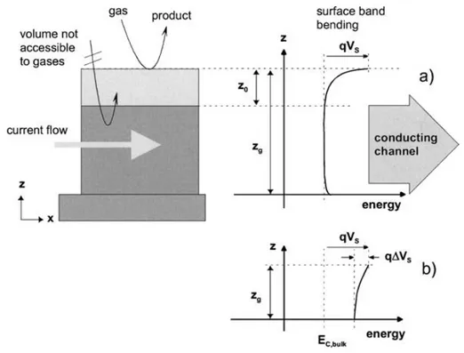
In the compact layer case, we may consider two different configurations: partially and completely depleted layer [11]. In the first case, when surface reactions do not influence the conductance of the whole layer (zg>z0 case, in Fig. 1.9), the conduction process takes
place mainly in the bulk (zg-z0 thick), which turns out to be much more conductive than
the depleted surface layer. This situation can be presented schematically with two parallel resistances: one influenced by surface reactions and the other not. Thus, the conduction is parallel to the surface and the reduced sensitivity is explained. The two configurations, partially and completely depleted layers, can switch one into the other, when in contact
Metal-oxide semiconductors: electronic behaviour and working mechanism
Figure 1.8: Schematic layout of a typical resistive gas sensor. The sensitive metal oxide layer is deposited over the metal electrodes onto the substrate. In the case of compact layers, the gas cannot penetrate into the sensitive layer and the gas interaction is only taking place at the geometric surface. In the case of porous layers the gas penetrates into the sensitive layer down to the substrate. The gas interaction can therefore take place at the surface of individual grains, at grain-grain boundaries and at the interface between grains and electrodes and grains and substrates.
Figure 1.9: Schematic depiction of a compact layer with geometry and energy band representa-tions: the thicker partially depleted layer (a) and the thinner completely depleted layer (b). z0
is the thickness of the depleted layer, zg is the total thickness and qVS is the band bending.
with oxidizing and reducing gases, respectively, because withdrawal or injection of free charge carriers occur.
For porous layers, the presence of necks between grains (see Fig. 1.11) complicates the situation. Three contributions may be present in a porous layer: surface/bulk (for large enough necks, which corresponds to zn>z0 in Fig. 1.11), grain boundary (for large grains
not sintered together) and flat bands (for small grains and small necks). The switching mentioned above for compact layers is also possible for porous ones.
In Fig. 1.10, we may observe the depletion area around grain surface and among in-tergranular contacts. The space charge region, depleted by charge carriers, is much more resistive than bulk, thus the layer close to the intergranular contacts is the main respon-sible for the resistance of the device. Considering the large grain model in Fig. 1.10, one notices that the charge carriers must overcome a potential barrier qVS, in order to move
electrons with energy at least equals to:
nS = NCe−(qVS+EC−EF)/kT = NDe−qVS/kT (1.19)
where NC represents the effective density of the states close to the bottom of the
conduc-tion band. Recalling Eq. 1.9, we may write: nS = NDeq
2N
S/2!!0kT Ni (1.20)
In the end, oxygen atoms adsorbed on the surface capture electrons from the bulk of the material, leading to the formation of a considerable potential, VS, which causes conduction
variation, monitored for gas detection.
The intermediate case between compressed particle and thin films occur when particles are syntherised, as can be seen in Fig. 1.11. The formation of necks occurs between syntherised particles. The more the neck diameter grows, the more the control of material conductance is assumed by the necks, rather than the surface states. This effect happens when neck size is comparable to the thickness of the space charge layer, that is to say that the diameter of necks must be 10 nm as order of magnitude. Therefore, an accurate control of grain morphology is necessary, in order to have reliable sensors for their quantitative use in real conditions [12].
1.3.3
Effects of adsorbed gases on electric resistance of sensors
Metal-oxide semiconductors are employed as chemoresistive gas sensors, because their elec-tric properties changes when gases interact with their surface. It is well-known that the electrical conductivity of metal oxides is dependent on gas adsorption. However, the in-terpretation of gas sensing mechanism is still controversial [13]. Two models have been proposed since now: the first one is based on oxygen ionosorption, while the second one on oxygen vacancies. Gas sensor response can be interpreted by both these mechanisms, which can be applicable at the same time [14].
At temperatures within 100◦C and 500◦C, the interaction between the surface of an
Metal-oxide semiconductors: electronic behaviour and working mechanism
Figure 1.11: Schematic depiction of a porous sensing layer with geometry and surface energy band-case with necks between grains: partially depleted neck (a) and completely depleted neck (b). zn is the neck thickness and z0 is depletion layer thickness.
form of molecular (O−2) and atomic (O− and O2−) ions. Ionosorption does not envisage
chemical bond: the adsorbate is electrostatically stabilised in the vicinity of the surface and acts as surface state, trapping electrons from the conduction band [7, 11, 14, 15]. Oxygen adsorption can be described by these simple reactions:
O2(gas) + e−! O−2(ads),
O2−(ads) + e− ! O22−(ads)! 2O−(ads)
(1.21) The molecular form is supposed to be dominant below 150◦C, while above this
temper-ature the atomic forms dominate [11]. However, we usually do not consider O2−, because
such a high charge on the ion can give instability, and O− is reckoned to be as the most reactive species in presence of reducing gases [7].
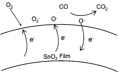
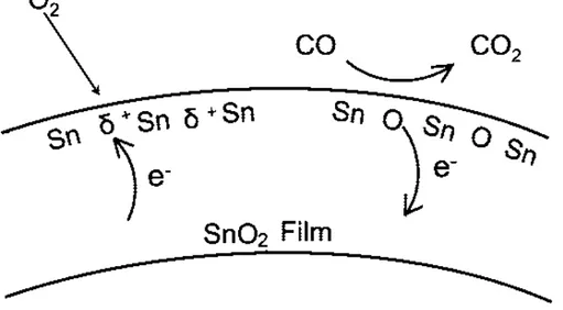
The presence of adsorbed oxygen ions leads to the formation of a depletion layer at the surface of tin oxide and to a high resistance. When reducing gases, such as CO, approach the surface of the sensor, they react with the oxygen ions and release electrons, which return to the conduction band. The final effect will be a decrease of resistance and thus increase of sensor conductivity. In an oxygen-free atmosphere, CO acts as electron donor: it is adsorbed as CO+ ion, thus releasing an electron in the conduction band [15]. Fig.
1.12 illustrate a scheme of ionosorption model.
The ionosorption model is widely accepted, even though is based mainly on phe-nomenological measurements and there is not yet any convincing spectroscopic evidence for ionosorbed oxygen species.
The oxygen-vacancy model is also consistent with most observations for semiconduc-tor metal oxide gas sensors [14, 15, 16]. In this model, as suggested by its name, oxygen vacancies at the surface of tin oxide are the determining factor in the chemoresistive be-haviour [16] and act as electron donors. Alternate reduction and reoxidation of the surface by gaseous oxygen (Mars-van Kravelen mechanism) control the surface conductivity and, therefore, the overall sensing behaviour. Three main steps can be specified: 1) CO removes oxygen from the surface of the lattice to give CO2, thereby producing an oxygen vacancy;
2) the vacancy becomes ionized, thereby introducing electrons into the conduction band and increasing conductivity; 3) if oxygen is present, it fills the vacancy; in this proccess one or two electrons are taken from the conduction band, which results in the decrease in
Metal-oxide semiconductors: electronic behaviour and working mechanism
Figure 1.12: Schematic depiction of ionosorption model for atmospheric O2 interaction and CO
gas sensing by SnO2.
conductivity. See Fig. 1.13 for a schematic depiction of this model.
The oxygen-vacancy model has not been discussed as widely as the ionosorption one, but numerous experimental and theoretical works have evaluated this explanation of gas-sensing effects, and it dominates in almost all spectroscopic studies.
Figure 1.13: Schematic depiction of oxygen-vacancy model for atmospheric O2 interaction and
Chapter 2
Gas adsorption processes
When a gas or vapour comes in contact with a clean solid surface, some of it will adhere to the surface in the form of an adsorbent layer. The solid is generally referred to as the adsorbent, the adsorbed gas or vapour as the adsorbate.
Any solid is capable of adsorbing a certain amount of gas. This quantity at equilibrium depends on the temperature, on the pressure of the gas and on the effective surface area of the solid. Therefore, the materials with the greatest adsorbent capacity are highly porous solids, such as charcoal and silica gel and finely divided powders. The relationship at a given temperature between the equilibrium amount of gas adsorbed and the pressure of the gas is known as the adsorption isotherm.
Adsorption reduces the imbalance of attractive forces which exists at a surface, and, hence, the surface free energy of a heterogeneous system.
2.1
Physisorption and chemisorption
Adsorption occurs when an attractive interaction between a gaseous particle and a solid surface is strong enough to overcome the disordering effect of thermal motion. Physical adsorption or physisorption takes place, if weak Van der Waals forces are involved in the interaction. Indeed, physisorptive bonds are characterised by dissociation energies below approximately 50 kJ/mol. Stronger forces are responsible for chemisorption and cause the formation of short chemical bonds with dissociation energies typically exceeding 50 kJ/mol.
Gas adsorption processes Since an activation barrier needs often to be overcome, chemisorption is considered an activated process [17, 18].
From a thermodynamic point of view, adsorption is a spontaneous process, which means that the change in free energy of the system is negative. The change in entropy is neg-ative, because the translational freedom of the adsorbate is reduced when it is adsorbed [19]. Therefore, considering the thermodynamic relationship:
∆G = ∆H− T ∆S < 0 (2.1) The enthalpy of adsorption, ∆Hads, must be negative. Thus, the adsorption of gases on
solids is an exothermic process. The extent of gas adsorption (under equilibrium con-ditions), therefore, increases with decreasing temperature. Exceptions may occur, if the adsorbate dissociates and has high translational mobility on the surface [19].
The equilibrium condition in physisorption is attained rapidly, since there is no activa-tion energy involved and the process is readily reversible. On the other hand, chemisorpactiva-tion may require an activation energy, as already written, and may, therefore, be relatively slow and not readily reversible. Fig. 2.1 illustrates a schematic potential diagram for the ad-sorption of a diatomic molecule of gas, X2, on a surface, M. Physisorption is described by
a Lennard-Jones potential, whereas chemisorption by a Morse potential.
The physical interaction energy includes a short-range negative (attractive) contribu-tion arising from London-Van der Waals dispersion forces and an even shorter-range posi-tive contribution (Born repulsion) due to an overlapping of electron clouds. In chemisorp-tion, the adsorbate, X2, dissociates to 2X. The dissociation energy of X2 (∆Edis) is
Figure 2.1: Potential energy curves for physisorption and chemisorption of a molecule X2 that
Gas adsorption processes
2.2
Adsorption isotherms
The extent of surface coverage is expressed as a fractional coverage θ: θ = N umber of adsorption sites occupied
N umber of adsorption sites available (2.2) The change of fractional coverage with time dθ/dt determines the rate of surface coverage or rate of adsorption.
The fractional coverage θ is in equilibrium with the free overlying gas. This equilibrium, which is dynamic because generated by two opposite processes (adsorption and desorption) occurring at the same rate, depends on the pressure of the free gas and on the temperature of the system. The variation of θ with pressure at a chosen temperature is represented by a curve, called adsorption isotherm. This function has a particular importance in the determination of information about the active surface of a material, as it will be observed further on. Several adsorption isotherms1 have proved to be useful in the understanding
of the adsorption process. However, the three isotherm equations most frequently used are those due to Langmuir, to Brunauer, Emmet and Teller (BET ) and to Freundlich.
2.2.1
The Langmuir isotherm
The Langmuir isotherm is based on the following characteristic assumptions: • adsorption of a single layer (monolayer coverage);
uncovered surface, expressed by (1-θ): dθ
dt = kap(1− θ) (2.3) where ka is the rate constant for adsorption.
The rate of desorption is proportional to the number of adsorbed species, represented by the surface coverage θ:
dθ
dt =−kdθ (2.4) where kd is the rate constant for desorption.
When adsorption equilibrium is established, θ is independent of time, thus both Eqs. 2.3 and 2.4 are equal. Solving this condition for θ, we obtain the Langmuir isotherm:
θ = Kp
1 + Kp (2.5) with K=ka/kd.
When considering a dissociative adsorption (X2(gas)'2X(surface)), the Langmuir isotherm
has a different form. In this case, the rate of adsorption is proportional to the pressure and to the probability that both atoms will find sites, that is to say the square of the number of vacant sites:
dθ
dt = kap(1− θ)
2
(2.6) The rate of desorption is proportional to the frequency of encounters of atoms on the sur-face, thus proportional to the square of the number of atoms present:
dθ
dt =−kdθ
2 (2.7)
Gas adsorption processes
Figure 2.2: Langmuir isotherms for dissociative (a) and non-dissociative (b) adsorption, for different values of K.
θ = (Kp)
1/2
1 + (Kp)1/2 (2.8)
The dependence of θ on pressure is weaker than in the case of non-dissociative adsorption. The trend of the Langmuir isotherms (see Figs. 2.2 for dissociative (a) and non-dissociative (b) adsorption, respectively) shows that the fractional coverage increases with increasing pressure and approaches one only at very high pressure, when the gas is forced on to every available site [19].
2.2.2
The BET isotherm
The Langmuir isotherm is well applicable in the situation of low coverage, but it fails at high adsorbate pressure, thus high coverage. Therefore, another mathematical expression is necessary to predict the case in which the initial adsorbed layer acts as a substrate for further adsorptions (i.e., physisorption). Multilayer adsorption has been treated by Brunauer, Emmet and Teller, who gave the name to the corresponding isotherm. The derivation of this model stands on the balancing of the rates of evaporation and condensa-tion for the various adsorbed molecular layers and on the assumpcondensa-tion that a characteristic heat of adsorption ∆Hads# applies for the first monolayer, while the heat of condensation ∆H#
con applies to adsorption in the second and subsequent molecular layers [17]. The BET
isotherm is usually written in the form: N Nmon = W Wmon = cz (1− z)1 − (1 − c)z (2.10) with z = p/p0, where p0 is the vapour pressure above a layer of adsorbate (considered as
a pure bulk liquid and thicker than a molecule). N and Nmon are the number of molecules
in the incomplete and completed monolayer, respectively, and W/Wmon is the weight
ad-sorbed relative to the weight adad-sorbed in a completed monolayer [20]. c is a constant depending on the extent of the enthalpy of adsorption compared to that of condensation: c∝ e(∆Hcon" −∆Hads" )/RT (2.11)
Since in multilayer coverage the vapour may condense to an unlimited extent, BET isotherms rise indefinitely as the pressure is increased, as shown in Fig. 2.3. The BET isotherm is reasonably valid over restricted pressure ranges, but it is not accurate at all values: it underestimate the extent of adsorption at low pressures and overestimates it at high pressures.
When c" 1, the BET isotherm takes the form: N
Nmon
= 1
Gas adsorption processes
Figure 2.3: BET isotherms for different values of c.
This expression describes the case in which adsorption is stronger than condensation. It is usually applicable to unreactive gases on polar surfaces [19].
One of the main application of BET theory is the determination of the surface area of solids, as reported with more details in App. A.
where c1 and c2 are constants, c2 usually being greater than unity.
Passing at the logarithms:
logV = logc1+ 1/c2logp (2.14)
Plotting logV versus logp, the result should be a straight line. This adsorption equation is a good interpretation of an adsorption model in which the variation of the magnitude of the heat of adsorption with surface coverage is exponential. The Freundlich isotherm attempts to take into account the role of substrate-substrate interactions on the surface.
2.3
The rates of surface processes
Adsorption and its reversing mechanism, desorption, are characterised by a combination of elementary kinetic steps. We may assist to non-dissociative (a diatomic molecule is adsorbed on a surface) or dissociative (a diatomic molecule fragments into atoms adsorbed independently) processes, which are also known as first and second order kinetics, respec-tively [21].
The interaction of a gaseous molecule with a solid surface is shown in Fig. 2.4, where the potential energy profiles of a molecule undergoing dissociative and non-dissociative adsorptions are depicted. The energy of the molecule approaching the surface decreases until a minimum, at which the molecule is physisorbed. This step is considered a precursor state for chemisorption, which may occur with or without dissociation [19]. In both cases, the energy initially increases, as the distance from the surface decreases and the bonds stretch (in the dissociative process) or adjust (in the non-dissociative process); after that, a sharp decrease of the energy indicates that adsorbate-substrate bonds reach their full strength. A potential energy barrier separates the precursor and the chemisorbed states in case of dissociative chemisorption, because an energy input is required to fragment the molecule. Therefore, dissociative chemisorption is an activated process and is slower than the non-activated kind.
The rate at which a surface is covered by adsorbate depends on the ability of the sub-strate to dissipate the energy of the incoming particle as thermal motion, as it crashes on to the surface. If the dissipation of energy is not quick, the particle migrates over the
Gas adsorption processes
Figure 2.4: Plots of potential energy versus distance for not activated (a) and activated (b) chemisorptions of a gaseous A molecule. P is the enthalpy of physisorption, C that of
chemisorp-surface until it is expelled by a vibration into the overlying gas or it reaches an edge. The probability that gas molecules stick onto the surface, i.e. the proportion of collisions with the surface that successfully leads to adsorption is called the sticking probability, s:
s = rate of adsorption of particles by the surf ace
rate of collision of particles with the surf ace (2.15) The denominator can be derived from the kinetic model, and the numerator can be deter-mined by observing the rate of change of the pressure.
The sticking probability varies widely and decreases as the surface coverage increases. A simple assumption is that the sticking probability is proportional to the fraction uncov-ered, 1-θ, and it is common to write:
s = (1− θ)s0 (2.16)
where s0 is the sticking probability on a perfect clean surface (zero coverage)
As already mentioned at the beginning of this chapter, adsorption is an exothermic process, thus it ultimately yields energy (energy of adsorption), even if it requires some energy input (activation energy) to initiate. Reversing adsorption, desorption, is always an activated process, because it requires an input of energy, corresponding to the depth of the potential well.
Desorption involves the time rate of change of the fractional coverage dθ/dt. This may also be viewed as the time rate change of the fraction uncovered, (1-θ).
The kinetic expressions for the rates of adsorption and desorption, expressed by Eqs. 2.6 and 2.7, can be written in a general way:
ra(θ) = dθ dt = kap(1− θ) n (2.17) rd(θ) =− dθ dt = kdθ n (2.18)
Gas adsorption processes n=1 we have a first order rate law for adsorption and desorption, for n=2 we have a second order process, which corresponds to dissociative adsorption and recombinative desorption of diatomic molecules.
If the rate constant for desorption is described by the Arrhenius equation, with ν pre-exponential factor or desorption frequency factor,
kd= νe(
−Edes
RT ) (2.19)
then we obtain a new expression for the rate law of desorption, also known as the Polanyi-Wigner equation [18]:
rd(θ) =−
dθ dt = νe
(−EdesRT )θn (2.20)
which is very useful in the determination of the activation energy of desorption, as it will be discussed in Ch. 4.
Chapter 3
Synthesis and deposition techniques
3.1
Synthesis of the nanostructured metal-oxide
powders
The sensitive materials used in the preparation of the chemoresistive gas sensors require specific characteristics. Since interactions with the gas phase occur on the surface, pre-cisely just below the solid-gas interface, a high specific surface area represents the first requirement, in order to enhance the sensitivity of the material. Therefore, the sensitive powder must be composed of nanometric grains (with mean radius of tens nm). The syn-thesis of metal-oxide powders is, thus, an important and delicate step of the whole process of sensor production.
The sol-gel technique was used for the preparation of the powders. Sol-gel is one of the most used method to synthesise a great variety of inorganic networks, employing silicon or other metal alkoxides as precursors. It is possible to prepare, at relatively low temperatures, materials based on inorganic oxides with the desired characteristics (hardness, chemical resistance, porosity and thermal resistance). The process consists mainly of three steps: it involves the hydrolysis of the organic precursor solution, the formation of a colloidal suspension and its evolution into a gel through condensation [22]. The structure of the final gel may differ, according to the variation of certain parameters, such as reaction temperature, water ratio and pH (acid or basic catalysis).
Synthesis and deposition techniques deionized water is added drop-wise to an n-butanol solution 0.7 M of tin(II)2-ethylexanoate, stirring it at room temperature for 3 h. The molar ratio of water to Sn is 4 and the pH of the solution is set at the unity with HNO3. The resulting gel is dried at 95◦C for 12 h in
order to obtain a yellow powder, which is subsequently calcined at 550◦C for 2 h [33]. Titanium butoxide (TB) is used as a source of titanium to synthesise the TiO2. TB
dis-solved in the absolute ethanol (0.23 M) is added drop by drop to a solution of ethanol/water 1:1 vol under mild stirring. This step is followed by 20 min of vigorous stirring. The ob-tained suspension is treated by means of the sol-gel process. After stirring, 16 h resting followed, the suspension was filtered to obtain a white precipitate, which is dried in air (100◦C) for 16 h. Finally, the powders are calcined at 400◦C in air for 2 h [34].
The solid solutions of Sn and Ti mixed oxide are produced via symplectic gel coprecip-itation (SGC) of stoichiometric Sn(4+) and Ti(4+) hydroalcoholic solutions and further calcination of the resulting xerogels. Calcination is performed at 550◦C for 2 h under
air-flow condition. The nanocrystalline powders obtained have a particle-size distribution which averages about 20nm, as determined by SEM [35]. The solid solutions of TixSn1−xO2
with different values of x (x=0.1, 0.3, 0.5, 0.7 and 0.9) will be hereinafter labeled as ST10, ST30, ST50, ST70 and ST90 [35]. Nb is added to the pure solution of Sn0.7Ti0.3O2 (ST30)
by coprecipitation, in the proportion of Sn:Ti:Nb=100:42:5 in order to enhance the con-ductivity. The resulting powder, named STN, is calcined at 400◦C for 2h.
3.2
The serigraphic process
Thick film technology, also known as serigraphic technology, is a wide-used manufacturing method, which differs from others for the film deposition process [23, 24]. It was introduced
three aspects.
• width of the deposition, thanks to the substitution of traditional masks into new ones made of steel and obtained by means of a laser, leading to films characterised by a minimum width of 20 µm;
• serigraphic pastes, whose improvement relies on the realisation of a great quantity of sensors, based on different functional materials;
• miniaturisation and compactness of the planar structures of thick films and multilayer configurations were recongnised to be appealing characteristics in the sensing field. However, the combination of the mass production capability to a relatively low cost (in comparison with other technologies) and the reliability of devices in difficult operating conditions make planar thick film technology one of the most suitable for sensors with the following requiremments:
• sensitivity to low pollutant concentrations; • reliability;
• repeatability;
• low energetic consumption; • moderate sizes;
• low ratio cost/performance; • automation possibility.
3.3
Production process of thick films
This section comprises the description of the main steps necessary to prepare thick films by means of the serigraphic technology. Some variations were performed in the Sensor and Semiconductor Laboratory of Ferrara, in order to obtain sensors well suitable for specific detecting demands. First of all, it must be underlined that the method employed
Synthesis and deposition techniques
Figure 3.1: Serigraphic machine equipped of a camera positioning system, operating in a clean room in order to avoid defects during deposition.
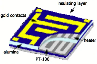
allows the deposition on the same substrate, not only of the sensitive film, but also of the heating elements, the interdigitated contacts and the elements necessary to the control of the sensor operating temperature. The serigraphic machine employed in the Sensor and Semiconductor Laboratory is shown in Fig. 3.1.
Figure 3.2: Multilayer configuration of the sensor. On the upper side, the sensitive layer is deposited among the comb contacts and represents an electric circuit lock. The self-adjusting temperature system, which consists of a variable resistor (Pt-100), is shown on the lower side.
the sol-gel technique, as already described (see Par. 3.1).
3.3.1
Preparation of the pastes
The functional phase is formed by:
• metal-oxide or semiconductor powder in case of resistive pastes; • metal or metal-oxide powder for the preparation of conductors; • vitreous or ceramic powder for the dielectric compositions.
The binder consists of a vitreous powder and has the function to promote film adhesion to the substrate after thermal treatment. The vehicle is a mixture of a resin and a volatile
Synthesis and deposition techniques solvent (medium) with the temporary binder function.
The ability to detect a few ppm of gas is assured by the fact that the functional material of the sensitive layer is made up of nanostructered metal-oxide powders, which control the electric and sensitive properties of the film. Indeed, the decrease of the particle size, from a micrometer order of magnitude to a nanometer one, emphasises important changes in the physical properties, which, in our case, comprise the interaction between film particles and gas molecules. Moreover, the highest ratio between surface and volume in nanometric materials makes surface properties become more important. Thus, these materials results to be particularly suitable for the detection of gas traces. Therefore, an accurate synthesis of those powders represents an important step in the preparation of the sensing film, taking into account many factors, such as shape and size of grains, their homogeneity, intergranular porosity and surface conditions [25, 26, 27].
Following the synthesis of the powders is the printing of the sensitive layer. This phase requires the preparation of a viscous paste, which is obtained adding an organic vehicle, consisting of a mixture of rheological agents (usually a resin made up of α-terpineol and ethyl-cellulose) in volatile solvents (for instance, 2(2-butoxyethoxy)ethyl acetate), to the nanometric powder. The composition of the organic vehicle gives printability to the paste, electrical and macroscopic morphological characteristics to the fired film. This ingredient is completely removed during the thermal processes, during which we assist to the formation of the microstructure of the deposited film. There is also a third constituent in the paste: a small quantity of inorganic binding agent, vitreous powders, helping the adhesion of the film to the substrate, and metal oxides, promoting the interdiffusion of particles during firing. On the whole, the preparation of the paste is a delicate step, because of the complexity of the system, which requires a certain number of components and involves specific phenomena in order to transform the deposited layers into functional
Figure 3.3: Scheme of the substrate, composed of its elements and layers.
employed substrate in thick film technology is alumina (96% Al2O3). A scheme of the
substrate is depicted in Fig. 3.3.
3.3.3
Printing
Printing on alumina substrates represents a fundamental step in the manufacturing process. This part of the process is performed by means of extrusion of the paste through the meshes of a screen (see Fig. 3.4. The paste is forced to go out, because of the decrease of viscosity caused by the pressure of the rubber-blade, which crosses the screen at a certain rate. The deposited layer may vary in a range of few up to 100 µm and depends on the following parameters:
• particle size; • paste viscosity;
• mesh number of the screen;
• strain of the steel threads that form the screen ; • rubber-blade hardness;
Synthesis and deposition techniques
Figure 3.4: Serigraphic screen, containing the substrates of alumina, where the deposition of the sensitive layers occurs. The frame must be projected in order to avoid deformations. The case depicted in this figure is characterised by a 20 N/cm strain and 300 meshes. The thread has a 18 µm diameter and the emulsion 25 µm. The minimum width for one line and for the resolution between adjacent lines is 100 µm order of magnitude.
• rubber-blade velocity;
• distance between screen and substrate (snap-off).
3.3.4
Drying up
A steady, definite and stable structure is, thus, obtained. Firing usually occurs in air, inside a muffle furnace, following temperature ramps suitable for each kind of sensor. Maximum temperature ranges from 600◦C up to 900◦C, according to the desired electrical and microstructural characteristics.
Chapter 4
Temperature-programmed desorption
measurements
Temperature-programmed desorption techniques are useful methods for the determination of kinetic and thermodynamic parameters of desorption processes. As the name of the method implies, the effects of temperature on surface reactions are involved. A sample is pre-treated to remove any adsorbed species from the active surface. Then, a gas is chemisorbed onto the active sites until saturation is achieved. After this first phase, the sample is heated with a temperature programme β(t)=dT/dt (with the temperature T usually being a linear function of the time t) and the signal corresponding to the atoms and molecules evolving from the sample is measured, e.g. by a mass spectrometer.
Temperature-programmed desorption (TPD) and intermittent temperature-programmed desorption (ITPD) turned out to be powerful characterising techniques for chemoresistive materials applied to gas sensing. ITPD is a differential form of TPD where a sequence of interrupted desorption runs is generated by means of a saw-tooth heating programme. It is an improved and well tested technique [28, 29], whose advantage consists in deducing the activation energy values in a simpler way compared to a single TPD profile.
Temperature-programmed desorption measurements
4.1
Theoretical model
Physical models of TPD are most often based upon a mass balance on the adsorption cell at quasi-steady state.
Recalling the Polanyi-Wigner equation for the rate law of desorption of kinetic order n (Eq. 2.20), we can write another expression, adding an adsorption contribution which takes into account the case of free readsorption [30]:
− dθ dt = νθ
ne(−Edes/RT )− µ(1 − θ)npe(−Eads/RT ) (4.1)
where µ is the preexponential factor of adsorption rate expressed in reciprocal pressure units, as frequently used for gases.
When a desorption experiment is performed under vacuum, the accumulation of the gas in the adsorption cell is considered negligible. Thus, the mass balance over the sample cell is defined by the following equation:
− qm
dθ
dt = Cp (4.2) where qm is the amount of gas adsorbed at saturation, p is the pressure of the gas above
the sample and C is the conductivity of the tube connecting the sample cell to the vacuum system (C = π3/2
8√2 D3
L
√RT
M , where D and L represent the inner diameter of the tube and its
equivalent length, respectively, M denotes the molar mass of the gas and T is the room temperature). A similar expression can be written for experiments carried out under an inert gas stream:
− qm dθ dt = qmνθne(−Edes/RT ) 1 + qmµ X (1− θ)ne(−Eads/RT ) (4.4) where X represents either C or F, according to the experimental case.
If free readsorption does not occur, the second term in the denominator of Eq. 4.4 is much smaller than 1 and the equation becomes:
−dθ dt = νθ
ne(−Edes/RT ) (4.5)
In this case, the energy E (obtained at quasi-constant coverage) is equal to the activation energy of desorption, Edes.
In the case of free readsorption, on the other hand, the second term is much larger than 1, so that another expression is obtained:
− qm dθ dt = Xν µ ( θ 1− θ) ne(∆H/RT ) (4.6)
where ∆H=Eads-Edes [30]. In this case, E is equal to -∆H.
Another way of writing Eq. 4.5 and 4.6 results useful, when calculating the preexpo-nantional factor:
− dθ dt = Ae
(−E/RT )f (θ) (4.7)
where, without readsorption, A=ν and f(θ)=θn; while in the case of free readsorption,
A=Cν
µqm and f(θ)=(
θ
1−θ)n [31].
The preexponential factor, also called frequency factor, is of great interest, when dis-cussing desorption experimental results (see Par. 4.3). We refer to the apparent energy of desorption, Eapp, when considering the experimental value, without knowing wether
read-sorption occurs or not. The related apparent frequency factor, Aapp, can be obtained using
Temperature-programmed desorption measurements Aapp = 1 Ntot dN dt exp Eapp RT (4.8)
where N is the amount of adsorbed species in a given state and Ntot is the amount of gas
necessary to saturate the considered state. Ntot and dN/dt are experimentally available
from the cumulative area of partial TPDs (when ITPD runs are performed) corresponding to the given state and from the measured desorption rate at the temperature T, respectively [32].
4.2
TPD and ITPD experiment
TPD and ITPD experiments were performed at IRCELYON (Institut de Recherches sur la Catalyse et l’Environnement de Lyon). Samples of SnO2, TiO2 and solid solutions of
them (TixSn1−xO2) were employed, in order to obtain information concerning their surface
properties. All the samples were prepared by the sol-gel method (see 3.1), except for SnO2 which was a commercial powder (CERAC). Specific surface areas of the samples
were measured according to the BET method by nitrogen adsorption at 77 K with samples previously evacuated at 300◦C under 10−1 mbar for 2.5 h. A Micromeritics TRISTAR 3000 was used for the purpose (see App. A for further details). Specific surface area values ranged from 8 to 115 m2·g−1 (see Tab. 4.1).
Table 4.1: Specific Surface Area values.
Figure 4.1: Picture of the experimental setup for vacuum TPD and ITPD.
4.2.1
Experimental apparatus
The experimental apparatus used for TPD and ITPD runs is a laboratory-built set-up schematically described in Fig. 4.1.
The sample (about 100 mg) was located in a cylindrical stainless steel sample holder (50 mm height and 4.0 mm in inner diameter) hanged in vacuum by K-type thermocouple wires (50 µm in diameter, spot-welded onto the sample holder) in the centre of a cylindrical quartz reactor. The powder was heated by means of a high-frequency system (1.1 MHz, 6 kW, manufactured by CFEI, France) with a 6-turn inductive coil placed around the reactor. A fast heating is assured with a small temperature gradient. Therefore, the sample holder is virtually thermally (except radiation mode) and mechanically isolated from both the reactor and the heating device.
The reactor can be evacuated down to 5·10−8 mbar by a turbomolecular pump and the
mass spectrometer is fitted with its own pumping system down to 1·10−7mbar. Analysis of
species released during desorption runs was carried out by a quadrupole mass spectrometer (Vggas Smart-IQ+).
Temperature-programmed desorption measurements
4.2.2
Description of the experiments
Each sample was first evacuated down to 1·10−6 mbar at room temperature and then
heated at 20 K·min−1 from room temperature up to 500◦C in pure O
2 under 133 mbar.
After the desired adsorption time (30 min), the sample holder was cooled down to room temperature under O2 and then evacuated to 10−6 mbar. After that, the reactor was
isolated from the vacuum line and directly connected to the MS through a large diameter UHV valve. The evacuation of the reactor was continued using a turbo molecular pump of the MS and the signals corresponding to the evacuated species were followed by the MS. The repetition of this procedure before each run insures that TPD runs were started at a nearly constant value of the oxygen-related MS signal corresponding to roughly 10−6 mbar
in the reactor. The TPD experiments were performed heating at 20 K·min−1. Desorbed
molecules were detected from room temperature to 850◦C, following the mass peaks at m/e=16, 18, 28, 32, and 44 amu. After TPD runs, samples ST30 and ST50 were chosen for ITPD experiments, which consisted in ”slicing” the complete TPD profile by means of a saw-tooth heating programmme. Temperature was increased to create oxygen partial TPDs, which were interrupted by temperature decreases. The heating rate of the ascendant part was 20 K·min−1. During the descendant parts, the sample was allowed to cool at a
higher rate in order to get the MS signal at m/e=32 back to its initial background level. Desorption was intermittent in this process.
the desorption of which is detected in the 400-850◦C range. Indeed, water and carbonates
are very stable species under O2 at 500◦C and block oxygen adsorption sites. Therefore,
as shown in Fig. 4.3, after the first desorption the surface was cleaned and more oxygen was adsorbed and desorbed during the second TPD run. Moreover, as oxides have to be fired at high temperature (in the 600-800◦C range) during the process to obtain the final sensing layer, it is evident that the first TPD is not representative at all of the properties of the material of interest. Therefore, only data from the second TPD were considered and corresponding profiles for samples SnO2, ST30, ST50, ST70, and TiO2 are shown in
Fig. 4.4. As one can notice, the SnO2 spectrum is characterised by the highest amount of
desorbed O2 with a composite desorption peak with maxima at about 570 and 730◦C, in
agreement with literature data [36, 37], while TiO2 seems to be the less performing powder
concerning the amount of released dioxygen. For STx samples, the amount of desorbed dioxygen increases when the amount of SnO2 in the mixed oxide increases (decrease of
x). Corresponding quantitative data are given in Tab. 4.2 and they also show that the amounts of oxygen species desorbed from sample STx are lower than those desorbed from SnO2, but do not correspond to a mere linear combination of (1-x)SnO2 / xTiO2. This
indicates the formation of a mixed oxide with different properties from both SnO2 and
TiO2. This conclusion is also supported by the shape of O2-TPD profiles from STx
sam-ples which are quite different from those of the Sn and Ti oxides. Except for SnO2 sample,
the desorbed oxygen amounts represent less than 10% of a compact monolayer of ions O−2 (corresponding to a theoretical maximal coverage of 13.7 µmol O2/m2 [38]). This result
excludes that oxygen is significantly desorbing from the bulk and indicates the presence of surface species, which play an important role in the solid-gas interactions.
Table 4.2: O2 desorbed quantities after the second TPD run.
Sample M ass (g) Desorbed O2 (µmol/m2)
ST 30 0.0986 0.20 ST 50 0.0947 0.10 ST 70 0.1374 0.06 SnO2 0.1368 1.98
Temperature-programmed desorption measurements
Figure 4.2: TPD profiles (signals at m/e = 18, 28, 32 and 44 amu) of the ST50 sample after the first O2 adsorption at 500◦C.
Figure 4.4: Complete O2-TPD profiles of the samples after the second O2 adsorption at 500◦C
(traces are offset to improve readability).
The apparent activation energy of desorption Eappand the associated frequency factors
Aapp corresponding to each adsorption state can be obtained by fitting the experimental
TPD profile (more precisely, a set of classical TPD first order or second order model peaks). However, such an approach is not reliable and an investigation by ITPD was preferred. The ITPD procedure may be better understood considering Fig. 4.5, where the heating programme and the corresponding series of partial desorption curves (MS signal at m/e = 32) are shown for ST50 sample submitted to oxygen adsorption at 500◦C. To check for the
reliability of the experiment, the sum of the area under each partial TPD was compared to the total area under the TPD curve presented in Fig. 4.4. The calculated values 1.9·10−7 and 1.7·10−7 A.s.mg
sample−1 for TPD and ITPD, respectively, are in satisfactory
agreement. The variation of MS signal at 32 amu versus temperature for ST50 sample is shown in Fig. 4.6 for the 21 partial TPDs, restricted to their ascending part in order to improve readability. The complete corresponding TPD is also shown on the same plot, in order to allow the localisation of four distinct zones corresponding to shoulder or peaks and labelled, α, β, γ, and δ, according to their order of appearance when temperature
Temperature-programmed desorption measurements increases.
Figure 4.5: Saw-tooth heating program and corresponding MS signal at m/e=32amu (ST50 sample).
Fig. 4.7 shows the Arrehenius plot of oxygen partial TPDs for ST50 sample, calculated from the curves shown in Fig. 4.6. The complete TPD is also presented in the Arrhenius plot. Obviously, in the Arrhenius plot of ITPD data, one can observe four families of lines, characterised by their average slope, and corresponding to the four shoulders or peaks, α, β, γ, and δ. Using least squares fitting, a regression was applied to the linear part of the Arrhenius transform of each partial TPD in order to calculate the apparent energy Eapp, which is directly proportional to the slope (-Eapp/R) of each line. The values of Eapp