UNIVERSIT `A DEGLI STUDI DI CATANIA FACOLT `A DI INGEGNERIA
Dipartimento di Ingegneria, Elettrica e dei Sistemi Tesi di Dottorato di Ricerca in Ingegneria Elettronica, Automatica
e del Controllo dei Sistemi Complessi (XXIII)
Umana Elena
IP2
C Transducers for
All-Organic Electronic Applications
Coordinatore: Prof. L. Fortuna Turor: Prof. S. Graziani Ing. M. La Rosa
Contents
Introduction . . . 1
1 Ionic Polimer-Polimer Composites . . . 3
1.1 Towards polymeric transducers . . . 3
1.2 IP2 C devices working principle . . . 5
1.3 Procedures for experiments on IP2 C . . . 6
1.3.1 Young modulus . . . 6
1.3.2 Characterization experimental setup . . . 8
2 Organic Electronics . . . 13
2.1 Organic electronics overview . . . 13
2.2 Testing platform . . . 16
2.3 Materials requirements and processing techniques . . . 17
2.4 Demonstrator . . . 22
2.5 Testbed architecture . . . 24
2.5.1 DC parameters of OTFT compact model . . . 25
2.5.2 AC parameters of OTFT compact model . . . 26
3 Organic Transducers Manufacturing using Different
Solvents . . . 31
3.1 Overview . . . 32
3.2 Manufacturing process . . . 33
3.2.1 Ethylene Glycol as solvent . . . 34
3.2.2 Ionic liquid as solvent . . . 35
3.2.3 Organic conductor . . . 36
3.3 Actuator electric characterization . . . 38
3.3.1 Actuator with EG as Solvent . . . 38
3.3.2 Actuator with EmI-Tf as solvent . . . 42
3.3.3 Dynamic Mechanical Analysis (DMA) . . . 45
3.3.4 Electromechanical transduction . . . 47
3.4 Sensor electric characterization . . . 50
3.4.1 Equivalent circuit of IP2 C sensor modeling . . . 54
3.5 Considerations . . . 57
4 New Techniques for Electrodes Deposition . . . 59
4.1 Organic electrodes manufacturing . . . 59
4.1.1 Chemical roughening . . . 60
4.1.2 Electrodes polymerization on Nafion R membranes . 61 4.2 Electromechanical characterization . . . 62
4.2.1 Actuator behaviour . . . 64
4.2.2 Sensor behaviour . . . 69
Contents IX
5 All-Organic Embedded System Design . . . 77
5.1 OTFT model implemented in CAD environment . . . 77
5.1.1 Static model . . . 79
5.1.2 Dynamic model . . . 80
5.2 All-organic conditioning circuit and peak detector design 82 5.2.1 Circuit simulation . . . 84
5.2.2 Layout . . . 86
5.3 Considerations . . . 87
Conclusions . . . 89
Introduction
This work focuses on the integration of polymeric transducers in or-ganic electronics applications. Two research environments have been exploited in order to realize a whole plastic motion transduction sys-tem, comprehensive of organic electronic control circuits. This kind of system has a huge potential since the two research environments com-bine the opportunity to develop low cost application with the possibility to use flexible substrates. A new class of mechanical transducers has been introduced: ionic polymer-polymer composites (IP2
Cs). These de-vices are realized by using only organic materials and manufactured by low cost processing techniques. They are based on Nafion R
membranes covered by organic conductors, like PEDOT:PSS. The investigation on organic technology has allowed to improve the performances of these polymeric transducers having both motion sensing and actuation prop-erties. In detail, their manufacturing processes have been reformulated in order to improve the transduction features and overcome the limi-tation due to the adopted materials. An in-deep investigation of poly-meric devices has allowed the development and implementation of a
first model of polymeric sensor in organic technology.
This research activity, from materials study and characterization for realization of organic thin film transistors (OTFTs) to its modeling in CADENCE environment, has allowed the simulation of different cir-cuits and the design of an embedded system for transduction. The design flow has been followed from schematic and simulation to layout. Chapter 1 introduces polymeric transducers, their working principle and the procedures for the analysis of their electromechanical pro-prieties. Chapter 2 gives a brief overview about organic electronics, describing the testing platform developed for the characterization of organic semiconductors. Chapter 3 reports an extensive study about all-organic electromechanical transducers. Different organic conductors for electrodes and two different solvents have been used, in order to overtake the limits imposed by organic materials and intrinsic charac-teristics of transducer. Chapter 4 describes a new technique for organic conductor deposition in order to enhance electrodes adhesion and to overtake the problems of hydration. In the Chapter 5 an embedded system has been designed combining organic electronics and polymeric transducers. The schematic and layout have been designed in CAD environment for further realization.
1
Ionic Polimer-Polimer Composites
In this chapter a brief introduction on polymeric transducers will be reported. Ionic Polymer-Polymer Composites (IP2
Cs) are a novel class of all-organic electroactive polymers that can operate both as electromechanical actuators and as sensors. They are an evolution of Ionic Polymer-Metal Composites (IPMCs), since the metallic layers, used to realize the elec-trodes, are substituted by using organic conductors, based on PEDOT:PSS.
1.1 Towards polymeric transducers
In recent years a wide interest has been devoted to the research on innovative materials for the development of flexible electromechani-cal transducers. More specifielectromechani-cally, electroactive polymers (EAPs) have been extensively investigated for their flexibility and lightness. Among these materials, Ionic Polymer-Metal Composites (IPMCs) have been demonstrated to exhibit sensing and actuation capabilities [1, 2, 3, 4].
IPMCs are constituted by an ion exchange perfluorinated membrane (e.g. Nafion R
115 or Nafion R
117), coated on both sides with a metallic electrode, generally a noble metal (such as platinum or gold). These metals are characterized by high cost and require complex deposition techniques in order to manufacture the electrodes. For these reasons, transducers with electrodes realized by using organic conductors [5], named Ionic Polymer Polymer Composites (IP2
Cs), have been intro-duced [6][7] and investigated. This new class of all-organic transducers exploits polymers that are becoming available and that are charac-terized by high conductivity values. They have already attracted re-searchers’ interest in various application domains from electronics to robotics or biochemistry organic conductors. In fact, organic conduc-tors are mainly processable from solutions and allow the use of low-cost deposition techniques such as spin-coating, dip-coating, spin-casting or printing techniques. In detail, the used organic conductor is PE-DOT:PSS characterized by a good conductivity (> 100 S/cm) and dif-ferent types have been synthesized, with increasing conductivity values. Some of them have been employed in order to the electrodes manufac-ture and to improve performances of devices.These devices present a layer structure as shown in Fig. 1.1: two layers of organic conductor cover the sides of Nafion R
membrane.
Fig. 1.1.Layer structure of a IP2
1.2 IP2
C devices working principle 5
1.2 IP
2C devices working principle
IP2
C actuation and sensing capabilities have been proved and their be-havior investigated. In the case of actuator bebe-havior, when a voltage is applied across the membrane thickness, it bends towards the anode side and the bending increases with the amplitude of the applied voltage. The obtained deformation is believed to be the result of two different contributions. The first one is due to the solvent (water or other sol-vents) molecules transport and is strictly linked to the ions that are free to move inside the polymer net; when an external voltage is ap-plied between the electrodes, the mobile cations, free to move inside the polymer net, move towards the cathode. If the membrane is hydrated, the cations carry with them solvent molecules, in a parasitical way. In this way the membrane cathode side increases its volume, while the anode region decreases its volume and hence contracts. The result is the bending of the strip towards the anode. A second contribution to the membrane deformation, when a voltage is applied, is supposed to depend on the charges distributed on the electrodes and could be due to the Coulombian interactions arising between charges in the organic conductor electrodes and the negative fixed charged groups belonging to the polymer matrix thus it strictly depends on the quality of the deposited electrodes.
The performance of the IP2
C transducer can be measured by the un-constrained free deflection of the device tip. The sensing capability has been demonstrated by measuring the inverse performance: the short
cir-cuit current voltage produced by the transducer when a deformation is applied. The relationship between induced current in the polymer results to be proportional to the mechanical deformation. The sensing capability of the device is dependent upon several factors, as such the frequency of the applied bending and the length of the transducer.
1.3 Procedures for experiments on IP
2C
The analyses of IP2
C electromechanical propriety have required the development of experimental procedures and devices in order to de-termine transduction features. The analysis of viscoelastic features of used polymer has been performed through the Dynamic mechanical analysis (DMA). Moreover, sensor and actuator behaviors have been studied and analyzed.
1.3.1 Young modulus
The behaviour of materials [8] of low relative mass is usually discussed in terms of two types of ideal materials: the elastic solid and the vis-cous liquid. The former has a definite shape and is deformed by external forces into a new equilibrium shape; on removal of these forces it reverts to its original form. The solid stores all the energy that it obtains from the external forces during the deformation, and this energy is available to restore the original shape when the forces are removed. By contrast, a viscous liquid has no definite shape and flows irreversibly under the action of external forces. One of the most interesting features of
poly-1.3 Procedures for experiments on IP2
C 7
mers is that a given polymer can display all the intermediate range of properties between an elastic solid and a viscous liquid depending on the temperature and the experimentally chosen time-scale. In de-tail Young modulus quantifies the elasticity of the polymer, it provides data about ability to deform of a material when a stress is applied to it. It is defined, for small strains, as the ratio of rate of change of stress to strain: E = σ
ε.
Young modulus is highly relevant in polymer applications involving the physical properties of polymers. Polymers have usually a viscoelastic behaviour. With low temperature, or high measurement frequencies, polymer can have a glassy behaviour and presents a Young modulus of 109
− 1010
Nm−2 and breaks with strain more than 5%. Whereas,
with high temperature, or low frequencies, polymer presents charac-teristics of a rubber and a Young modulus of 106
− 107
Nm−2, that
can undergo high stretch(about 100%) without permanent strain. In case of middle values of temperature and frequencies (glassy transi-tion range), the polymer behaviour does not exhibit rubber or glass feature and can dissipate, straining, a considerable amount of energy. Dynamic Mechanical Analysis (DMA), is a technique used to study and characterize materials which is most useful for observing the vis-coelastic nature of polymers. The experimental procedure consists in subjecting the specimen to an alternating strain and simultaneously measure stress. For linear viscoelastic behaviour, when equilibrium is reached, the stress and strain are expressed by the following equations:
ε(t) = ε(ω)eiωt (1.2) where ω is the angular frequency. The measures of strain and stress provide complex modulus values E∗(ω), defined through the followed
expression:
σ(ω) ε(ω) = E
∗(ω) = E0(ω) + iE00(ω) (1.3)
where E0(ω), which is in phase with strain, is called the storage
modulus because it defines the energy stored in the specimen due to the applied strain. While E00(ω), which is π/2 out of phase with the
strain, defines the dissipation of energy and is called the loss modulus, because the energy (∆E) dissipated per cycle can be computed as:
∆E = πe2 0E
00 (1.4)
The ratio between storage and loss modulus defines the damping factor: tanδ = E
00
E0 (1.5)
The DMA analysis of IP2
C samples has been performed by means of Tritec 2000 DMA produced by Tritec Technology (thanks to the collaboration with DMFCI of Universit`a degli Studi di Catania) shown in Fig. 1.2. A force (stress) is applied to the sample. The stress is transmitted through the drive shaft onto the sample which is mounted in a clamping mechanism.
1.3.2 Characterization experimental setup
The experimental setup has been realized ad hoc in order to character-ize the device behavior. In case of actuators, a voltage signal is used to
1.3 Procedures for experiments on IP2
C 9
Fig. 1.2.Tritec 2000 DMA equipment.
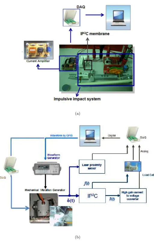
deform the membranes, while in case of sensors, a displacement is ap-plied obtaining, a short-circuit current. The scheme of the experimental setup realized for the actuator characterization, including the data ac-quisition section, shown in Fig. 1.3. A buffer (realized via an OPA548) was needed to deliver the required current which is of the order of hundreds of milliamperes to the actuator, while the instrumentation amplifier (INA111) was used to measure the absorbed current, by us-ing the shunt resistor Rs. The IP2C tip displacement was measured by
using a laser distance sensor (Baumer Electric OADM 12). Data were acquired by a National InstrumentsT M USB-6008 multifunction DAQ
card and sent to a computer.
Fig. 1.4 shows two different schemes of setup used to perform the sensor characterization. In detail, Fig. 1.4(a) reports a first measure-ment setup used to observe sensor operation. In fact, it allows to deter-mine sensing current of a membrane that is strained through a impul-sive impact system. The other experimental setup (Fig. 1.4(b)) allows to analyze and determine more information about sensing behavior.
Fig. 1.3. Experimental setup scheme for actuating measurements.
Moreover, it can apply different signals to the vibrating system, in or-der to observe and analyze membrane behaviour.
In a first phase the electromechanical capabilities of IP2
C sensor have been tested using a mechanical apparatus designed to impose the membrane deformation by periodic impulsive impacts, shown in Fig. 1.4(a). It is composed by a moving cylindrical bumper made of plastic, actuated by a CC motor through a gearing system and a slider. The plastic bumper hits the IP2
C membrane alternating the face of the impact. The periodic impacts cause a sensing current flowing through the short-circuit amplifier that is acquired by a computer, through a DAQ card. In a second set of experiments , the mechanical stimulus was imposed to the IP2
C membrane by means of the programmable me-chanical vibration generator system (TIRA Schwingtechnik TV50009) shown in Fig. 1.4(b). The mechanical vibration generator was driven by a voltage signal produced by an arbitrary function generator or directly by a computer, through the DAQ card, in case of a tailored signal. The mechanic wave was transmitted to the membrane through two copper electrodes which are printed inside the clamps. They allow
1.3 Procedures for experiments on IP2
C 11
also to sense the IP2
C short-circuit current by means of a high gain current to voltage amplifier based on LF411 operational amplifier (con-ditioning circuit). At the other side of the strip, a load cell (Transducer Techniques GSO-10) has been used to measure the blocking force. Fur-thermore, the displacement δ has been measured close to the clamp by using a laser distance sensor (Baumer Electric OADM 12). The signals measured by the current amplifier, the load cell and the laser sensor were recorded by means of a National Instruments USB-6008 multifunc-tion DAQ card. A graphical user interface, developed under LabviewT M
environment, has been developed in order to drive the multifunction DAQ card. Moreover, it allows to display and make a first analysis of recorded signals. Data were processed by suitable Matlab R
scripts that will be described in following chapters.
(a)
(b)
2
Organic Electronics
The development of post silicon technologies, based on or-ganic materials, consolidates the possibility to realize new de-vices and applications with unusual properties: e.g. flexibility, light weight, disposability. Both materials and processes play a fundamental role in this new electronic framework and have been improved continuously in the last decades. In this chap-ter a complete framework for characchap-terization and modeling of organic semiconductor materials is reported [9]. Multifunc-tional testbeds have been developed to analyze different or-ganic semiconductors through hybrid demonstrators of mul-tilayered structure devices.
2.1 Organic electronics overview
Since the realization of the first Organic Thin Film Transistor in 1983 [10], an intense research effort has been dedicated to both the improvement of organic materials and development of innovative
de-position and manufacturing techniques for low cost electronics assess-ment. Up to now organic thin film transistors have been investigated for applications in different fields from electronic backplanes in organic light-emitting diodes (OLED) for rollable displays, to chemical and bio-FET sensors, to simple logic circuits, to be associated with radio-frequency identification (RFID) tags, as well as with thin- film batter-ies and e-paper in new multi-functional systems [11, 12, 13]. Organic material properties have been tailored to obtain required features for electronic applications by designing new molecules with enhanced prop-erties, improved lifetime and environmental stability, as well as solu-tion processability and feasible charge mobility. Thus, the possibility to modify the composition and material preparation is the strongest turn of post silicon technologies in the electronic application field. Thanks to the improvements obtained in recent years, organic semiconductors exhibited charge mobility values comparable to amorphous silicon and polysilicon [14, 15, 16]. On the other hand, stamp-based imprinting processes are going down to tens of nanometers in scale, without the high costs of conventional lithography. Nanoimprint Lithography (NIL) and Soft Lithography (SL) processes [19], [20], based on hard and soft stamps respectively, are continuously improved and equipment manu-facturers are investing to realize machineries to manufacture organic devices on large area. Imprinting lithography, combined with low-cost deposition techniques like spin-coating and inkjet printing, are cur-rently adopted to realize multilayered structures of materials processed by solution. The combination of the former aspects, materials and
pro-2.1 Organic electronics overview 15
cess, paves the way to the fabrication of new active and passive devices for advanced applications. In this perspective, a consolidated work-flow going from materials to devices is required considering a complete Technology Platform that describes the process flow-chart and the tools used in the design, layout and realization of an organic electronic cir-cuit. The basic elements which define the organic technology platform are: organic materials, manufacturing process techniques and the CAD framework [21]. The fundamental element of organic electronics is the Organic Thin-Film Transistor (OTFT), developed by different organic materials: conductors, dielectrics and semiconductors. Therefore, ma-terials characterization is an important step towards the realization of organic technology devices.
A testing platform has been designed. The behavior of polymer semi-conductors has been analyzed through the characterization of single devices such as transistors or logic gates. Moreover, multifunctional testbeds architectures have been designed following the IEEE Standard 1620-2004 ”Characterization of Organic Transistors and Materials”. Hybrid organic structures have been adopted to obtain a standard semi-conductor polymers benchmarking. The characterization of the organic semiconductors and the related model OTFT have been performed and device parameters extracted [22].
2.2 Testing platform
The adopted testing platforms for organic electronics are hardware/software systems composed by application demonstrators and testbed. The de-sign processes of demonstrator and testbed follows a sequence of steps according to the application definition as reported in Fig. 2.1.
Fig. 2.1.Testing platform design flow. Copyright [2009]EDP Sciences.
The application description, by identifying its characterizing ele-ments and its main functionalities, is the first step of the testing plat-form design.The choice of the application architecture is heavily af-fected by materials manufacturing techniques. Organic material depo-sition, synthesis and patterning impose technological limits, to be con-sidered during test platform design. Moreover, any manufacturing tech-nique needs exploiting specifics equipments which influence designing
2.3 Materials requirements and processing techniques 17
choices. In this phase technological data (materials, substrate typolo-gies, etc.), operative information (functionalities) and general technical specifics (processing techniques, feature sizes, etc.) are defined. In the next step developed ad hoc demonstrators are described with relative interface systems.
2.3 Materials requirements and processing
techniques
Some interesting properties of organic materials such as lightweight, flexibility, ease of manufacturing and low processing costs, motivated an intense research in innovative materials scouting. Organic semiconduc-tors have been extensively studied for long time but only recently they have attracted a more increasing interest, according to the possibility to use them as active layers in Organic Thin Film Transistors. Organic semiconductors can be mainly classified according to the type of charge carriers, which can be holes (p-type) or electrons (n-type). Up to now the lack of feasible electron-transporting n-type materials, which are very sensitive to the environment, hindered the development of organic CMOS technology, thus only p-type materials have been adopted and only ratioed logic p-type circuitries have been designed [23]. The re-search is actually ongoing toward the improvement of new n-type mate-rials exhibiting highest charge carrier mobility and air stability. Organic semiconductors can also be classified in small molecules and polymers. Among small molecules, oligothiophenes, phthalocyanines, pentacene
and tetracene, generally present good electrical performances, thanks to their high molecular order. However, they are generally insoluble and solution processing techniques cannot be adopted. Evaporation or vacuum deposition process through shadow masks are required with higher costs and higher energies than additive solution manufacturing processes. On the other hand, the class of polymers known as con-jugated polymers, characterized by π-concon-jugated backbone structures containing many double bonds, has shown semiconductor features. Or-ganic semiconductor polymers are of particular interest for innovative applications, being solution processable by very low cost deposition techniques such as spin-coating, dip-coating, or inkjet printing. How-ever, most of these polymers are generally characterized by disordered structures with poorer electrical performances. Nevertheless, the pos-sibility to use solution processing techniques makes them the preferred material for organic electronic development. As concerns the organic conductors, the research in this field has been highly increased since 1977 with the discovering by Shirakawa, MacDiarmid and Heeger for which where awarded in year 2000 with the Nobel Prize in Chemistry. They discovered the ability to dope polymers in the full range from insulator to metal [24]; in particular, they found out that films of poly-acetilene (trans-(CH)x), p-doped by treatment with an oxidizing agent such as gaseous bromine or iodine, exhibited an increase in conductiv-ity of many orders of magnitude, passing to a ”metallic state”. Among available conducting polymers, PEDOT:PSS exhibits the highest con-ductivity values, i.e. in the order of magnitude of hundreds of siemens
2.3 Materials requirements and processing techniques 19
per centimeter. It can be deposited from solution through low cost de-position and patterning techniques such as spin coating, dip coating and various printing techniques such micro Contact Printing (µCP ) or inkjet printing. The availability of organic materials with both conduct-ing and semiconductconduct-ing features paved the way to the development of the organic electronic technology whose primary component is the Or-ganic Thin Film Transistor. In particular, the possibility of manufactur-ing it through solution and patternmanufactur-ing steps in a multilayer functional structure (Fig. 2.2), make them alternative to the traditional inorganic Silicon based electronics. The electric performances are not compara-ble to the inorganic counterpart but the opportunity to adopt them for realizing economic, large area, innovative applications is highly ap-pealing. The prime key for organic electronic technology development is represented by the availability of a set of organic materials (semi-conductors, (semi-conductors, dielectrics) with good electrical and chemical characteristics and compatible solvents.
The adopted organic materials must satisfy some requirements which strongly affect the OTFT performances: organic conductors with large conductivities are required for the realization of source and drain contacts; organic semiconductors with high charge carrier mobility and high Ion/Ioff ratio are needed to ensure high current values and low leakages; as concerns the adopted organic dielectric, high-k materials are required as gate dielectrics, while low-k dielectrics are needed as or-ganic insulating materials. Since the interface among gate dielectric and semiconductor is the active area where charge transport takes place, the
Fig. 2.2.Multilayer functional structure of OTFT and interconnections.
presence of defects act as traps. A semiconductor/dielectric interface with imperfections and an increased roughness implies a decreasing of mobility and device performances. Moreover, the development of post silicon devices based on organic materials implies a deep investiga-tion of the main issues to obtain feasible devices in terms of stability, robustness and efficiency. Many organic materials, such as, e.g., the organic semiconductor Poly3-HexylThiophene (P3HT), have stability problems in air due to the interaction with the external environment and need coating to be protected from oxygen or humidity. Parallel to material scouting, an intense research is also focused on the im-provement of deposition and patterning techniques together with large scale manufacturing of flexible organic devices at low cost. In partic-ular, imprinting manufacturing processes, enabling the downscaling of feature sizes, are investigated to guarantee the realization of circuits with the necessary switching speed. Among the imprinting techniques,
2.3 Materials requirements and processing techniques 21
two main methodologies can be recognized: the NanoImprint Lithog-raphy (NIL) techniques and the Soft Lithographic (SL) ones. These techniques are both based on an imprinting process: NIL process uses an hard stamp generally made in Silicon or UV transparent quartz with feature sizes down to tens of nanometers; the Soft Lithographic pro-cess makes use of a soft stamp of poly(dimethylsiloxane) (PDMS) which limits the minimum feature size achievable to hundreds of nanometers. Hard moulds with patterned relief structures are used in both NIL and SL techniques. Moulds are fabricated by conventional processes (optical lithography, e-beam lithography, dry and wet etching, etc.) and can be used many times to produce soft stamps or to pattern directly polymer films. Detachment of patterned films is made possible by anti-sticking treatments of molds [25]. The Fig. 2.3 reports molds master in silicon wafer, with minimum feature size of 200 nm, used for NIL.
Fig. 2.3.Molds master in silicon wafer.
The manufacturing of a soft stamp is performed by pouring the PDMS over the hard mould, degassing of the poured PDMS in air,
cur-Fig. 2.4. Flexible mold PDMS replica.
ing in oven and finally by peeling-off. The PDMS stamp replicates the silicon mould structures, as shown in Fig. 2.4. Several PDMS stamps can be obtained from silicon moulds thus decreasing the cost related to imprinting manufacturing. The selection between hard and soft stamp patterning is strictly related to the employed materials and the de-sired geometric feature size. More in details, the NIL technique allows obtaining smaller feature sizes, by using different types of patterning methods: Hot Embossing and UV-Based. The first applies high pres-sure and heats the material with temperatures higher than the glass transition temperature Tg of the adopted material. The second is used for organic materials curable by UV radiation.
2.4 Demonstrator
Demonstrators based on metallic contacts with a silicon substrate have been used to obtain templates for organic semiconductors testing. Used
2.4 Demonstrator 23
demonstrator architectures are thin film transistor (Fig. 2.5(a)) and logic gate(Fig. 2.5(b)) with different feature sizes.
Fig. 2.5.Template of pseudo-pmos organic TFT(a) and inverter(b).Copyright [2009]EDP
Sciences.
In order to investigate the device behavior different geometrical pa-rameters (such as the channel length and the gate dielectric thick-ness) have been considered. These structures allow the deposition of different organic semiconductor to be tested. Pads and via intercon-nections have been designed for guaranteeing the electrical contacts with the characterization equipment by means of a probing system. Logic gates have been designed adopting a conventional pseudo-pMOS architecture which uses only p-type organic transistors. These config-urations are mainly constituted by a driver circuit implementing the logic function and a load circuit usually constituted by a transistor operating in the saturation region. Once the application architecture design is completely developed, its validation becomes essential; for
this reason it is necessary the development of multifunctional testbeds. Testbeds are software/hardware systems able to interact with demon-strator samples, designed to implement a set of test protocols. Testbed architecture design can be accomplished through the identification of a set of test parameters. Three main components define the testbed ar-chitecture: test protocols, measurement/probing instruments and data lodging systems.
2.5 Testbed architecture
The testing parameters have been defined through the specification of different measurements. The gate leakage curves (IGSvs VGSand IGDvs
VGD) characterize the gate dielectric quality and quantify leakage
cur-rent from the gate to the channel. Leakage measurements are carried out to ensure gate dielectric integrity before subsequent measurements are performed. The transfer curves (IDS vs VGS) allow the preliminary
determination of field-effect mobility (µ) and threshold voltage (VT).
The output curves (IDS vs VDS) provide saturation and OTFT
elec-trical performance information and are used to determine whether the device exhibits FET-like behaviour. The capacitance curves (CGD vs
VGS and CGS vs VGS) are obtained by the sum of two capacitive
con-tributes: the gate to channel capacitance and the stray capacitance. The stray capacitance values (due to geometrical overlapping of drain source contacts with gate plate) have a negative effect on device switch-ing speed and may affect device electrical characterization. In order to
2.5 Testbed architecture 25
obtain the required set of measurements, a dedicated multifunctional system, comprising probing, measuring and lodging instruments, has been implemented.
2.5.1 DC parameters of OTFT compact model
A specific strategy has been defined to extract OTFT parameters using electrical measurements. A compact model of organic transistors and a complete characterization of the organic semiconductor have been obtained. The method consists of a differential analysis of the transfer characteristic curves (ID vs VGS) and exploits the different functional
dependencies of current on gate voltage which is induced by the pres-ence of contact resistances. Using the expression of drain current in the linear regime:
ID = K(VGS− VT)γ+1VDS (2.1)
and taking into account the effects of RS and RD, letting VGS = VG,
the following quantity which does not depend on RSD is obtained:
z = I 2 D I0 D = K γ + 1(VG− VT) γ+2 VD (2.2) w = RVG VT zdV 0 G z ∼= RVG 0 zdV 0 G z = 1 γ + 3(VG− VT) (2.3) The threshold voltage VT, the mobility parameter K and the
source-drain resistance RSD can be extracted by using the quantities z and
VT γ RSD K −1.2 V 0.613 1.5 MΩ −8.76e − 9 F/Vs
Table 2.1. Parameter values obtained through used method.
The parameter values obtained by transfer curves have been em-ployed in the compact model implemented in CAD environment. Sim-ulated OTFT behaviours have been compared with experimental data as reported in Fig. 2.6.
2.5.2 AC parameters of OTFT compact model
Dedicated methods have been implemented to extract capacitance val-ues through experimental data fitting. Fig. 2.7 represents experimental data of device impedance.
From the impedance analysis of experimental data different be-haviours of gate-drain and gate-source impedances have been obtained. Moreover, a parametric study, using different impedance models (two RC parallel elements, three R series-RC parallel elements, four elements with Warburg impedance) has been carried out [28]. Results have been used to validate device impedance behavior with different polarization conditions. In particular, experimental conductance and capacitance mostly showed high variability respect to frequencies variations. Circuit analysis has been performed using the impedance frequency response characteristics in terms of both Bode and Nyquist analysis.
2.5 Testbed architecture 27 −20 −18 −16 −14 −12 −10 −8 −6 −4 −2 0 −2.5 −2 −1.5 −1 −0.5 0x 10 −6 V gs [V] Id [A] −20 −18 −16 −14 −12 −10 −8 −6 −4 −2 0 −4 −3 −2 −1 0x 10 −6 V gs [V] Id [A] Simulation data V d = −10V Experimental data V d=−10V Simulation data V d= −5V Experimental data V d = −5V −20 −18 −16 −14 −12 −10 −8 −6 −4 −2 0 −5 −4 −3 −2 −1 0x 10 −6 Id [A] V gs [V] −20 −18 −16 −14 −12 −10 −8 −6 −4 −2 0 −5 −4 −3 −2 −1 0x 10 −6 V gs [V] Id [A] Simulation data V d = −15V Experimental data V d = −15V Simulation data V d = −20V Experimental data V d = −20V
Fig. 2.6.Experimental and simulation data of OTFT. Copyright [2009]EDP Sciences.
Equivalent impedance model, with relative characteristic parame-ters, have been identified by fitting simulated Nyquist plot with exper-imental data (Fig. 2.8).
102 103 104 105 104 105 106 107 108 |Z| [ Ω ] V GS=−40 V V GS=−35 V V GS=−30 V V GS=−25 V V GS=−20 V V GS=−15 V V GS=−10 V V GS=−5 V V GS= 0 V V GS= 5 V V GS=10 V V GS=15 V V GS=20 V 102 103 104 105 −1.5 −1 −0.5 0 phase(Z) [Rad] frequency [Hz]
Fig. 2.7.Measurements of impedance phase and module. Copyright [2009]EDP Sciences.
0 0.5 1 1.5 2 2.5 3 3.5 x 10⁶ −14 −12 −10 −8 −6 −4 −2 0 x 105 V DS=−25 ReZ [Ω] ImZ [ Ω ] Experimental data V gs=0V Model V gs=0V Experimental data V gs=5V Model V gs=5V Experimental data V gs=10V Model V gs=10V Experimental data V gs=15V Model V gs=15V Experimental data V gs=20V Model V gs=20V
Fig. 2.8. Measured impedance and equivalent model fitting. Copyright [2009]EDP
2.6 Considerations 29
2.6 Considerations
The aim of this work was the development of a complete organic testing platform for organic device validation. A technology platform CAD flow has been defined to design organic circuits and layout, starting from OTFT model.
3
Organic Transducers Manufacturing using
Different Solvents
The integration of IP2
C into all-organic electronic circuits have required a study about transducer performances. In this chapter an investigation of possible solvents for IP2
C mem-branes has been performed in order to increase their perfor-mances [29]. For the IPMC based actuators it is generally reported that solvents, different from water, can be used to avoid the dehydration phenomenon. In the same way, in this chapter the possibility to use Ethylene Glycol and an ionic liq-uid, 1-Ethyl-3 Methylimidazolium Trifluoromethanesulfonate, as diluents for IP2
C is investigated. Moreover, different ma-terials have been used for device electrodes manufacturing and the performances of different organic transducers have been compared. Several devices have been realized and char-acterized by Scan Electrodes Microscopy (SEM) and Dynamic Mechanical Analysis (DMA). Their electromechanical behav-ior as actuators and sensors have been analyzed and a suitable material set has been identified.
3.1 Overview
All-organic electromechanical transducers, based on Nafion R
117 as ionomer membrane, have been manufactured using different formula-tion of poly (3,4-ethylendioxythiophene)-poly (styrenesulfonate) (PE-DOT:PSS) as electrode material.
If water is used as solvent for IP2
Cs they experience water loss that causes several limitations in term of performance and applications. In fact, the applied electric potential must be limited to less than 1.3V at room temperature, to avoid electrolysis and water evaporation in open air. Moreover, organic electrodes can degrade during sample hy-dration in the solvent. These problems can be overcome by using other than water solvents. E.g, Ethylene Glycol (EG) that, as water, consists of polar molecules, or 1-Ethyl-3 Methylimidazolium Trifluoromethane-sulfonate (EmI-Tf), that is an ionic liquid existing as liquid at room temperature and shows high inherent stability [30] have been proposed for the case of IPMCs and will be taken into account here for IP2
Cs. Moreover, it is known that an enhancement in the conductivity can be obtained by adding to the conducting polymer different organic com-pounds (called secondary dopants or additives) such as several alcohol (diethylene glycol, 2-nitroethanol, glycerol) or high-boiling-point sol-vents (dimethyl sulfoxide, dimethylformamide, tetrahydrofurane). It is therefore possible to argue that to use EG and Ionic Liquids (ILs) in IP2
Cs, instead of water, can cause a beneficial effect on the electrical conductivity of PEDOT:PSS films. The conductivity enhancement is
3.2 Manufacturing process 33
strongly dependent on the changes of the chemical structure of the organic compounds, in particular on the conformational change that the secondary dopants determine into the polymer chains: the driving force is the interaction between the dipoles of the organic compound and dipoles or charges on the PEDOT chains [17]. Upon addition of EG or IL, conducting PEDOT:PSS grains merge together to form a three-dimensional conducting network [31], [32] determining an improvement of its electrical property. Moreover, an important difference between ILs and the high-boiling-point solvents, previously used as additives, is that ILs are not volatile and thus remains in the polymer conducting films. By substituting in the IP2
Cs the water with EG or an IL it is there-fore possible to obtain both all-organic devices with low manufacturing cost, to overcome the dehydration problem and to improve electrical performance because of the enhancement of the electrical conductivity of PEDOT:PSS used as electrode. Different IP2
C prototypes have been manufactured and have been analyzed both morphologically through Scanning Electron Microscopy (SEM) and electrically, showing their electromechanical transduction behavior.
3.2 Manufacturing process
All-organic transducers have been realized based on a fluorocarbon membrane, Nafion R
117 (produced by Dupont R
and distributed by Sigma-Aldrich Group, membrane thickness is 178 µm). The adhesion quality in thin film deposition strongly depends on surface properties;
for this reason, before the conductor deposition, Nafion R
surface has been roughened. In order to remove water from the Nafion R
mem-brane, it was dried at 100◦C for 24 hr, then it has been kept in vacuum
for 3 hr.
3.2.1 Ethylene Glycol as solvent
In the first experiment, Ethylene Glycol (EG) was used as solvent for the Nafion R
based IP2
Cs. Ethylene glycol viscosity is about 16 times higher than that of water at room temperature, and has a greater molecular weight. It is used as an anti-freezer. Like water, it consists of polar molecules and has been already suggested to be used as a solvent for IPMCs [33]. In Table 3.1 some chemical properties of EG are reported [34]. While Fig. 3.1 shows the chemical structure of EG [35].
Properties
Relative Density 1.109 g/ml
Molecular weight 62.07 g/mol
Boiling Point 197.6◦C Water solubility at 17.5◦C 10 g/100 ml Melting point -13◦C Dielectric constant at 20◦C 41.4 Viscosity at 25◦C 16.1 · 10−3 P a · s
Table 3.1.Some properties of ethylene glycol.
In order to obtain the IP2
Cs with EG as solvent, Nafion R
mem-branes have been roughened and dried, soaked overnight in a beaker containing pure EG and, finally, heated to 60◦C for 3 hr.
3.2 Manufacturing process 35
Fig. 3.1.Chemical structure of Ethylene Glycol.
3.2.2 Ionic liquid as solvent In a second experiment, IP2
Cs using an ionic liquid as solvent have been produced. Ionic liquids are salts containing only charged species that exist in their liquid state at room temperature. They have an im-measurably low vapour pressure, electrochemical stability windows of 4 V or more, and are thermally stable to temperatures as high as 400◦C.
Furthermore, ionic liquids have high ionic conductivities and can be used as electrolytes for a variety of applications, including electrochem-ical capacitors [36] and conducting polymer actuators [37]. The ionic liquids are used as solvents for Nafion R
based transducers for their stability and, therefore, to avoid the problem of solvent evaporation. Also, the ionic liquids are ionically conductive and should therefore fa-cilitate ionic motion in the Nafion R
membrane. In this work 1-ethyl-3 methylimidazolium trifluoromethanesulfonate (EmI-Tf) has been used: it has a viscosity of 35 · 10−3 Pa· s - 45 · 10−3 Pa· s at 25◦C. The more
relevant properties of EmI-Tf are reported in Table 3.2 and in Fig. 3.2 its chemical structure is showed [38].
Properties
Relative Density at 25◦C 1.387 g/ml
Molecular weight 260.23 g/mol
Water solubility fully soluble
Boiling Point > 350◦C
Melting point 263-264 K (-9◦C)
Ionic conductivity 8.6-9.3 mS/cm
Electrochemical stability window 4.1 V
Table 3.2.Some properties of EmI-Tf.
Fig. 3.2.Chemical structure of EmI-Tf.
To produce IP2
Cs with EmI-Tf as solvent, Nafion R
membranes have been soaked, after roughing and drying, overnight in a beaker containing pure EmI-Tf and then heated to 140 ◦C for 3 hr.
3.2.3 Organic conductor
Poly (3,4-ethylendioxythiophene)-poly (styrenesulfonate) (PEDOT:PSS) is one of the best known conducting polymers: it shows excellent electri-cal conductivity as well as processability. E.g., for the case of CleviosT M
3.2 Manufacturing process 37
this work, IP2
Cs have been fabricated using different formulations of PEDOT:PSS, reported in Table 3.3, to realize the electrodes.
Organic Conductor Trade Name Material Supplier
PEDOT:PSS
CLEVIOST M PH 500
CLEVIOST M P HC V4 H.C.Starck
CLEVIOST M PH 510
Orgacon REL-P 3040 AGFA
Table 3.3. Adopted conducting materials.
The conducting polymers have been applied on the Nafion R
sur-face by drop-casting technique, since it is a very low cost procedure: the polymer has been spread over both sides of the Nafion R
mem-branes (after they have been processed by using either EG or EmI-Tf, as described in the previous sub-sections). Eventually, IP2
Cs have been dried with an extractor fan and heated to 60◦C for 2 hr. Eight different
IP2
Cs were produced and they are listed in Table 3.4 along with used sample codes.
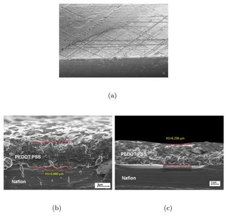
Surface analysis of the samples has been performed by SEM in or-der to evaluate the layer adhesion and the film thickness. In Fig. 3.3 two SEM images of an IP2
C section are reported. More specially, these figures show a sample with Orgacon R
EL-P 3040 electrode, whose thick-ness is about 6 µm - 7 µm, while the thickthick-ness of Nafion R
117 mem-brane is 178 µm. Fig. 3.3(a) shows tilted view and (b)-(c) report two
Organic material Solvent Sample code
CLEVIOST M PH 500 EG EG-PH500
CLEVIOST M PH 500 EmI-Tf EmI-PH500
CLEVIOST M P HC V4 EG EG-PHCV4
CLEVIOST M P HC V4 EmI-Tf EmI- PHCV4
CLEVIOST M PH 510 EG EG-PH510
CLEVIOST M PH 510 EmI-Tf EmI-PH510
ORGACON REL-P 3040 EG EG-3040
ORGACON REL-P 3040 EmI-Tf EmI-3040
Table 3.4. Samples manufactured and tested.
cross-section view of two samples. It is possible to observe that the PEDOT:PSS surface is highly inhomogeneous and rough.
3.3 Actuator electric characterization
Obtained IP2
Cs were cut into strips of size 2 cm x 0.5 cm and their electromechanical transduction capabilities were tested. More specifi-cally, the free deflection produced was investigated. EmI-PH510 and EG-PH510 samples did not show good actuating performance, for this reason their characterization will not be reported in the following.
3.3.1 Actuator with EG as Solvent
A common set of experiments was defined for the IP2
C characteriza-tion and the evaluacharacteriza-tion of the suitable organic conductors to be used. A sinusoidal voltage signal with a frequency sweep from 50 mHz to 50 Hz
3.3 Actuator electric characterization 39
(a)
(b) (c)
Fig. 3.3.SEM images of an IP2
C tilted view (a)and cross sections(b)(c).
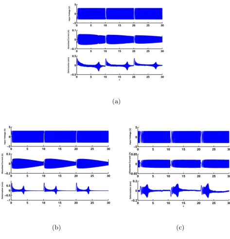
or 150 Hz and amplitude 3 V were applied to all samples and the cor-responding absorbed current and sample displacement were measured and acquired. Data were used to estimate the IP2
C voltage to deforma-tion transfer funcdeforma-tion of sample displacement and to evaluate sample’s resonance frequency, in the hypothesis that a linear approximation for the IP2
C can be used.
Data recorded for EG-PH500, EG-PHCV4 and an EG-3040 are re-ported in Fig. 3.4. A perusal analysis of signals rere-ported allows to conclude that the actuating behavior of the sample with Orgacon R
EL-0 5 10 15 20 25 30 −5 0 5 Input Voltage (V) 0 5 10 15 20 25 30 −0.1 0 0.1
Absorbed Current (A)
0 5 10 15 20 25 30 −0.5 0 0.5 Deformation (mm) s (a) 0 5 10 15 20 25 30 −5 0 5 Input Voltage (V) 0 5 10 15 20 25 30 −0.2 0 0.2
Absorbed Current (A)
0 5 10 15 20 25 30 −1 −0.5 0 0.5 Deformation (mm) s (b) 0 5 10 15 20 25 30 −5 0 5 Input Voltage (V) 0 5 10 15 20 25 30 −0.05 0 0.05
Absorbed Current (A)
0 5 10 15 20 25 30 −0.2 0 0.2 Deformation (mm) s (c)
Fig. 3.4. Actuator frequency sweep measurement with EG-PH500 (a), EG-PHCV4 (b)
and EG-3040 (c).
P 3040 electrodes (EG-3040) is very poor, when compared with the behavior of other samples. It is, in fact, possible to observe that a very small and noisy deflection was obtained for the EG-3040 sample. As a further investigation, the magnitude of the voltage to deflection trans-fer functions for the same samples is seen in Fig. 3.5. For EG-PH500 the resonance frequency is about 76 Hz. This sample has the highest
3.3 Actuator electric characterization 41
resonance frequency, since the EG-PHCV4 sample resonance frequency is about 56 Hz, while EG-3040 resonance frequency is about 12 Hz.
10−1 100 101 102 −80 −70 −60 −50 −40 −30 −20 −10 0 Magnitude [dB] frequency [s] EG−3040 EG−PH500 EG−PHCV4 (a)
Fig. 3.5. Transfer function magnitude of PHCV4(blue), PH500(green)and
EG-3040(magenta).
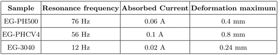
Sample Resonance frequency Absorbed Current Deformation maximum
EG-PH500 76 Hz 0.06 A 0.4 mm
EG-PHCV4 56 Hz 0.1 A 0.8 mm
EG-3040 12 Hz 0.02 A 0.24 mm
Table 3.5.Obtained values of absorbed current, deformation and resonance frequency of
IP2
Cs with EG.
Table 3.5 reports values of resonance frequency, absorbed current amplitude and maximum deformation values of the three tested IP2
Cs with EG.
3.3.2 Actuator with EmI-Tf as solvent
In a second set of experiments, the behavior of samples with EmI-Tf as solvent and with the organic conductors (see Table 3.4) were inves-tigated, by using the same experimental conditions described in the previous sub-section: a swept voltage signal was applied to the samples EmI-PH500, EmI-PHCV4, and EmI-3040 and absorbed current and tip free deflection were recorded. Time records are shown in Fig. 3.6, while the corresponding transfer function magnitudes are reported in Fig. 3.7.
EmI-PHCV4 and EmI-PH500 have close resonance frequency and resonant peak amplitude values, whereas EmI-3040 shows both lower resonance frequency and resonant peak amplitude values.
3.3 Actuator electric characterization 43 0 5 10 15 20 25 30 −5 0 5 Input Voltage (V) 0 5 10 15 20 25 30 −0.1 0 0.1
Absorbed Current (A)
0 5 10 15 20 25 30 −1 0 1 Deformation (mm) s (a) 0 5 10 15 20 25 30 −5 0 5 Input Voltage (V) 0 5 10 15 20 25 30 −0.02 0 0.02
Absorbed Current (A)
0 5 10 15 20 25 30 −0.5 0 0.5 Deformation (mm) s (b) 0 5 10 15 20 25 30 −5 0 5 Input Voltage (V) 0 5 10 15 20 25 30 −0.05 0 0.05
Absorbed Current (A)
0 5 10 15 20 25 30 −0.5 0 0.5 Deformation (mm) s (c)
Fig. 3.6. Actuator frequency sweep measurement with EmI-PH500 (a), EmI-PHCV4 (b)
100 101 −80 −70 −60 −50 −40 −30 −20 −10 0 Magnitude [dB] frequency [Hz] EmI−3040 EmI−PH500 EmI−PHCV4
Fig. 3.7.Transfer function magnitude of PHCV4(blue), PH500(green)and
EmI-3040(magenta).
Sample Resonance frequency Absorbed Current Deformation maximum
EmI-PH500 41.6 Hz 0.06 A 0.4mm
EmI-PHCV4 39 Hz 0.02 A 0.7 mm
EmI-3040 18.4 Hz 0.031 A 0.27mm
Table 3.6.Obtained values of absorbed current, deformation and resonance frequency of
IP2
Cs with EmI-Tf.
Table 3.6 reports values of the resonance frequency, absorbed cur-rent amplitude and maximum values of sample deformation obtained by tested IP2
Cs with EmI-Tf.
Results reported so far have shown that IP2
C that use CleviosT M
P HC V4 and P H500 gave best results in terms of applied voltage to produced deformation. Moreover, IP2
C based on PHCV4 showed better results in terms of stability. For such a reason in the following this last
3.3 Actuator electric characterization 45
class of devices will be in deeper analyzed to investigate the effects of EmI-Tf and EG on IP2
C behaviour.
3.3.3 Dynamic Mechanical Analysis (DMA)
DMA is a very versatile technique which can provide a convenient and sensitive testing system for rapid determination of thermo-mechanical properties of polymers and polymer-based materials as a function of frequency, temperature or time. The measurements were performed by means of Tritec 2000 DMA produced by Tritec: a sinusoidal ten-sile force was applied to the samples (in hydrated condition) in the range from 0.1 to 100Hz, at working temperature T=20 C. Measure-ments of the storage modulus and loss modulus (E’ and E”) as well as the damping parameter or loss factor (tanδ), defined as the ratio tanδ=E”/E’, were obtained to compare the influence of the solvent in the mechanical properties IP2
Cs. It is important to take into account that elastic moduli measured by DMA often does not agree well with those obtained from mechanical testing methods [40]. In most cases, the elastic moduli measured by DMA are utilized only for screening material properties for the purposes of quality control, research and development of optimum processing conditions. Fig. 3.8(a) shows the DMA results for the storage modulus (E’) of Nafion R
, EG Nafion R
, EG-PHCV4 as a function of frequency in tensile mode. Fig. 3.8(b) re-ports the results for the storage modulus (E’) of samples with EmI-Tf. Fig. 3.9 shows the Loss moduli (E”) of Nafion R
, EG Nafion R
, EG-PHCV4, EmI Nafion R
tensile mode. Finally, Fig. 3.10 reports the tanδ of Nafion, EG Nafion, EG-PHCV4, EmI Nafion and EmI-PHCV4.
(a) (b)
Fig. 3.8. Storage modulus (E’) of Nafion, EG Nafion and EG-PHCV4 Nafion (a); EmI
Nafion and EmI-PHCV4(b) as a function of frequency.
(a) (b)
Fig. 3.9. Loss modulus (E”) of Nafion, EG Nafion and EG-PHCV4 Nafion (a); Nafion,
EmI Nafion and EmI-PHCV4(b) as a function of frequency.
By comparing the data relative to Nafion R
with those of the other samples, it is evident that the presence of the solvent has a plasticizer effect leading to the reduction of the tensile strength by disconnecting
3.3 Actuator electric characterization 47
(a) (b)
Fig. 3.10. tanδ of Nafion, EG Nafion and EG-PHCV4 Nafion (a); Nafion, EmI Nafion
and EmI-PHCV4 as a function of frequency.
the membrane polymer chains and determining a volume change of base materials. The presence of the electrode (conducting polymer) determines an increase in the modulus value.
3.3.4 Electromechanical transduction In this section, the two IP2
C considered in the previous subsection are investigated with respect to their electromechanical transduction. The frequency behaviour of IP2
Cs has been tested by using a set of three consecutive swept signals. The magnitudes of the transfer functions of the two samples are shown in Fig. 3.11(a) and (b), respectively. Experiments have shown that, at least for very short repetition times of the experiments, the frequency response of the devices are quite close one each other. More specifically a good agreement has been obtained for the values of their resonance frequency.
101.4 101.5 101.6 101.7 101.8 −50 −45 −40 −35 −30 −25 −20 −15 −10 Magnitude [dB] frequency [HZ] first measurement second measurement third measurement (a) 101.4 101.5 101.6 101.7 101.8 −50 −45 −40 −35 −30 −25 −20 −15 −10 Magnitude [dB] frequency [Hz] first measurement second measurement third measurement (b)
Fig. 3.11. Consecutive measurements of a EG-PHCV4 sample (a) and a EmI-PHCV4
sample (b).
The transfer function magnitudes of the two samples are compared in Fig. 3.12. The EmI-Tf sample displays a lower magnitude than the sample with EG. Also resonance frequency obtained with EG is higher.
3.3 Actuator electric characterization 49 100 101 102 −60 −50 −40 −30 −20 −10 0 Magnitude [dB] frequency [Hz] EG−PHCV4 EmI−PHCV4
Fig. 3.12. The magnitudes of the transfer functions of EG-PHCV4 and EmI-PHCV4
3.4 Sensor electric characterization
Sensor behaviour has been tested for all kinds manufactured mem-branes with different electrodes and solvents discussed previously. Moreover, also deionized water has been used for transducers and inves-tigated in this section. The sensor has not problem of water hydrolysis and, therefore, the membranes did not need to be rehydrated. More-over, IP2
C sensor works in good condition when the sample is not very hydrated. For this reason, samples with water as solvent have been characterized and their sensing currents have been reported.
The experimental setup of Fig. 1.4(a) has been used in order to de-tect the performances of polymeric sensors. The Fig. 3.13 shows sens-ing currents produced by samples with deionized water applysens-ing peri-odic impulsive impacts. The interesting result is that the sample with ORGACON R
EL-P 3040 shows the best result in term of sensing cur-rent than other samples. As it will be shown in following results only in this case ORGACON R
EL-P 3040 allows to IP2
C to produce higher current than other organic conductors.
3.4 Sensor electric characterization 51 0 2 4 6 8 10 −0.6 −0.5 −0.4 −0.3 −0.2 −0.1 0 0.1 0.2 0.3 Sensing Current ( µ A) s (a) 0 2 4 6 8 10 −1.5 −1 −0.5 0 0.5 1 Sensing Current ( µ A) s (b) 0 2 4 6 8 10 −1.5 −1 −0.5 0 0.5 1 1.5 Sensing Current ( µ A) s (c)
Fig. 3.13. Sensor measurement with H2O-PH500 (a), H2O-PHCV4 (b) and H2O-3040
(c).
The Fig. 3.14 show sensing currents produced by PHCV4, EG-PH500 and EG-3040 samples applying periodic impulsive impacts.
Fig. 3.15 show sensing currents produced by PHCV4 , EmI-PH500 and EmI-3040 samples applying periodic impulsive impacts.
These sensor measurements allow to detect the devices that pro-duce the larger sensing current for the same applied deformation. In detail, the sample with ORGACON R
0 1 2 3 4 5 6 7 8 9 10 −7 −6 −5 −4 −3 −2 −1 0 1 2 3 Sensing Current ( µ A) s (a) 0 2 4 6 8 10 −6 −4 −2 0 2 4 6 8 Sensing Current ( µ A) s (b) 0 10 20 30 40 50 60 70 80 90 100 −0.8 −0.6 −0.4 −0.2 0 0.2 0.4 0.6 Sensing Current ( µ A) s (c)
Fig. 3.14.Sensor measurement with EG-PH500 (a), EG-PHCV4 (b) and EG-3040 (c).
a smaller current than other devices both with EG and EmI-Tf. More-over, from the graphs of the sensing currents it is possible to notice that the EG solvent produced samples with better performances than EmI-Tf membranes. These analyses are determinant in order to iden-tify the organic conductor for electrodes and the solvent to be used to obtain good sensing performances.
3.4 Sensor electric characterization 53 0 2 4 6 8 10 −5 −4 −3 −2 −1 0 1 2 3 4 5 Sensing Current ( µ A) s (a) 0 2 4 6 8 10 −6 −4 −2 0 2 4 6 Sensing Current ( µ A) s (b) 0 1 2 3 4 5 6 7 8 9 10 −0.25 −0.2 −0.15 −0.1 −0.05 0 0.05 0.1 0.15 0.2 Sensing Current ( µ A) s (c)
3.4.1 Equivalent circuit of IP2C sensor modeling
In order to develop novel smart applications the electromechanical transducers have been characterized and its behavior has been modeled. The polymeric composite sensing device has been modeled by defining the dynamical system that transforms the applied mechanical stimulus into the sensor electric reaction. The IP2
C membranes demonstrated sensor capabilities to detect mechanical deformation. An IP2
C sensor device structure is shown in Fig. 3.16, where f (t) is the applied force, δ(t) is the deflection of the beam and IS(t) obtained in short-circuit
condition.
Fig. 3.16.Parameters characterizing the actuator and sensor devices
An electric equivalent circuit has been obtained starting from the electromechanical model [41] of the IP2
C sensor described by Equa-tion 3.1.
I(s) = k3tkwY 4Ls
· s
3.4 Sensor electric characterization 55
The circuit, shown in Fig. 3.17, comprises an RC structure, intro-duced to model the intrinsic capacitive nature of the membrane.
Fig. 3.17.Electric equivalent circuit of IP2C sensor model.
Two resistances Re has been introduced in order to model the
or-ganic conductor resistive effect. Moreover the resistance R1 has been
introduced to model the equivalent bulk resistance of Nafion R
in DC conditions. In order to parameterize the model as a function of membrane dimensions the resistance R1 is expressed in terms of the
Nafion R
DC resistivity ρ1 and the geometrical parameters as defined
by Equation 3.2.
R1 =
ρ1· tk
LT OT · w
(3.2) The value of ρ1 in agreement to Dupont datasheets is 1205Ωm. The
capacitors C has been expressed in terms of the permittivity ε and membrane geometric quantities according to the relation 3.3.
C = ε ·LT OT · w tk
(3.3) The organic electrodes resistance Re is also expressed by
Equa-tion 3.4 as a funcEqua-tion of the membrane dimensions and suitable pa-rameter RS
Re = RS·
LT
w (3.4)
The value of RS has been obtained from the identification procedure
reported in [9]. The electromechanical transduction has been modeled by means of the voltage source generator Vδ controlled by the
displace-ment δ(t). The term β is a proportionality coefficient which models the coupling between the input displacement and the voltage applied to ca-pacitor C. The relations which associate the electric circuit parameters ε and β to the electromechanical model parameters of Table 3.4.1 are expressed by Equation 3.5 and Equation 3.6 where RP is the equivalent
parallel resistance between R1 and 2Re.
ε = tk LT OT · wαRP (3.5) β = 3 2tkY kRS (3.6) Y k α 4.6027(GP a) 2.1373 · 10−8(CsN−1 ) −13.0838(Hz)
3.5 Considerations 57
The obtained normalized circuit parameter values are reported in the Table 3.4.1.
RS β ε
52.5806(Ωm/m) 1.5514(V /m) 6.226 · 10−4(F/m)
Table 3.8. Equivalent circuit parameters.
The sensor model, reported in [9], has been described in order to explain its implementation in CADENCE R
environment, reported in Chapter 5.
3.5 Considerations
In this chapter the electromechanical transduction properties of differ-ent IP2
Cs have been compared. Samples have been manufactured by using several conducting polymers and different solvents. More specifi-cally, solvents, different from pure water, have been taken into account in order to overcome its limits: the used solvents allow to use higher voltage values and to avoid the hydration phase that is incompatible with some organic conductors. The IP2
C shows better performances with CleviosT M P HC V4 and with CleviosT M PH 500 both during
ac-tuator and sensor characterization. Moreover, both solvents allow trans-ducers to obtain considerable actuating behavior, but better features have been observed with EG than EmI-Tf. In case of sensor behaviour EG solvent allows to obtain higher values of current.
4
New Techniques for Electrodes Deposition
The research activity on polymeric transducers was focused on increasing their performance overcoming the limits of samples hydration. New manufacturing techniques have been taken in account in order to allow soaking in solvents. In this chap-ter, other methods for electrodes manufacturing have been investigated to permit the rehydration after actuator or sen-sor electromechanical functioning. Moreover, these techniques have permitted to use water as solvent in devices with con-ductors that solve in water.
4.1 Organic electrodes manufacturing
In previous chapters the adhesion problem of polymer conductor was discussed. In fact, the Nafion R
sample was processed through the sandblasting in order to limit the problem. This processing consists in membrane roughening where organic conductor was deposed by drop casting technique. In Fig. 4.1 two SEM images are reported showing
that conductor layer is not totally adhered to Nafion R
membrane. More-over, during hydration phase, when samples are soaked in solvent, af-ter few seconds, the conductor layers peel off Nafion R
. When water is employed as solvent for actuator IP2
C the rehydration destroys the sample.
(a) (b)
Fig. 4.1.SEM images where organic electrode is teared out from Nafion membrane.
For these reasons other techniques for Nafion R
processing and for organic conductor deposition have been analyzed and employed.
4.1.1 Chemical roughening
This technique allows to increase the quality of adhesion of organic con-ductor with Nafion R
membranes. It is based on chemical roughening by treatment with sulfuric acid (H2SO4) and hydrogen peroxide (H2O2).
The chemical roughening consists in boiling Nafion R
membranes in a solution of sulfuric acid, H2SO4 1M (under stirring) for a half hour,
![Fig. 2.1. Testing platform design flow. Copyright [2009]EDP Sciences.](https://thumb-eu.123doks.com/thumbv2/123dokorg/4510808.34496/22.918.198.648.283.614/fig-testing-platform-design-flow-copyright-edp-sciences.webp)

![Fig. 2.5. Template of pseudo-pmos organic TFT(a) and inverter(b).Copyright [2009]EDP](https://thumb-eu.123doks.com/thumbv2/123dokorg/4510808.34496/29.918.240.701.179.401/fig-template-pseudo-pmos-organic-tft-inverter-copyright.webp)
![Fig. 2.6. Experimental and simulation data of OTFT. Copyright [2009]EDP Sciences.](https://thumb-eu.123doks.com/thumbv2/123dokorg/4510808.34496/33.918.239.697.102.675/fig-experimental-simulation-data-otft-copyright-edp-sciences.webp)
![Fig. 2.8. Measured impedance and equivalent model fitting. Copyright [2009]EDP Sci-](https://thumb-eu.123doks.com/thumbv2/123dokorg/4510808.34496/34.918.188.648.541.820/fig-measured-impedance-equivalent-model-fitting-copyright-edp.webp)