Autore:
Eleonora Marchetti _______________
Relatori:
Prof. Luca Fanucci ___________________ Prof. Roberto Saletti ___________________
Enhancements of MEMS design flow for
Automotive and Optoelectronic
applications
Anno 2010
UNIVERSITÀ DI PISA
Scuola di Dottorato in Ingegneria “Leonardo da Vinci”
Corso di Dottorato di Ricerca in
INGEGNERIA DELL’INFORMAZIONE
ACKNOWLEDGMENTS
I am a lucky woman, many are the people which have supported me during my course of study and during the three years of my PhD, but I have no doubt about which are the first two person whose I want to say thank you, my parents, because after many years of studies they are yet the “best teachers” that I have never had. A big thank you is for the rest of my family, my wonderful sister Laura and her husband Michele which have always supported me and believed in me.
And a not smaller thank you is for another very important person in my life: Francesco which has constantly followed me during these years with his love and especially with his patient.
I would like also say thank you to the best friend that I have never had, Manuela for her friendship, complicity and constant support.
Then my gratitude goes to my tutors Prof. Luca Fanucci and Prof. Roberto Saletti both for their precious technical help, for the several chances of professional improving they provided to me, and their friendship.
A special thank goes to the SensorDynamics AG design centre of Navacchio (with particular appreciation to the R&D team and the evaluation team), the people working there taught me what is commitment and professionalism, but I can consider them as good friends too.
And a finally thank is for the research center Fraunhofer Institute for Silicon Technology where I have found several chances to improve my work.
ABSTRACT
In the latest years we have been witnesses of a very rapidly and amazing grown of MicroElectroMechanical systems (MEMS) which nowadays represent the outstanding state-of-the art in a wide variety of applications from automotive to commercial, biomedical and optical (MicroOptoElectroMechanicalSystems). The increasing success of MEMS is found in their high miniaturization capability, thus allowing an easy integration with electronic circuits, their low manufacturing costs (that comes directly from low unit pricing and indirectly from cutting service and maintaining costs) and low power consumption.
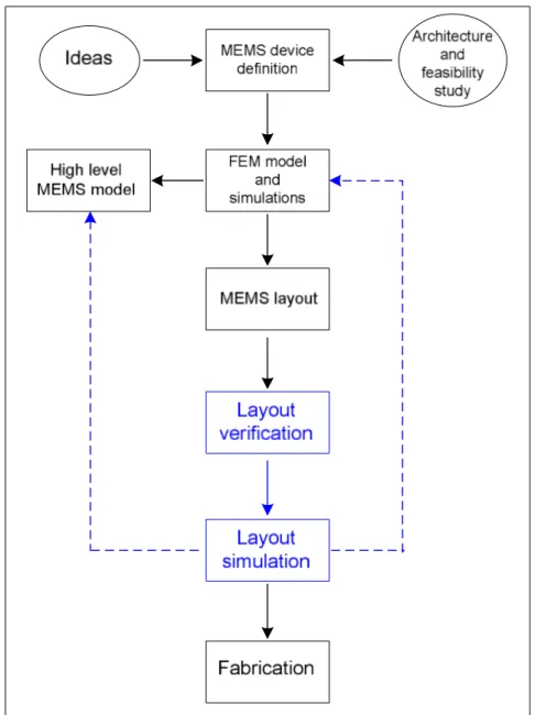
With the always growing interest around MEMS devices the necessity arises for MEMS designers to define a MEMS design flow. Indeed it is widely accepted that in any complex engineering design process, a well defined and documented design flow or procedure is vital.
The top-level goal of a MEMS/MOEMS design flow is to enable complex engineering design in the shortest time and with the lowest number of fabrication iterations, preferably only one. These two characteristics are the measures of a good flow, because they translate directly to the industry-desirable reductions of the metrics “time to market” and “costs”.
Like most engineering flows, the MEMS design flow begins with the product definition that generally involves a feasibility study and the elaboration of the device specifications. Once the MEMS specifications are set, a Finite Element Method (FEM) model is developed in order to study its physical behaviour and to extract the characteristic device parameters. These latter are used to develop a high level MEMS model which is necessary to the design of the sensor read out electronics. Once the MEMS geometry is completely defined and matches the device specifications, the device layout must be generated, and finally the MEMS sensor is fabricated.
In order to have a MEMS sensor working according to specifications at first production run is essential that the MEMS design flow is as close as possible to the optimum design flow.
The key factors in the MEMS design flow are the development of a sensor model as close as possible to the real device and the layout realization. This research work addresses these two aspects by developing optimized custom tools (a tool for layout check (LVS) and a tool for parasitic capacitances extraction) and new methodologies (a methodology for post layout simulations) which support the designer during the crucial steps of the design process as well as by presenting the models of two cases studies belonging to leading MEMS applications (a micromirror for laser projection system and a control loop for the shock immunity enhancement in gyroscopes for automotive applications).
SOMMARIO
Negli ultimi anni abbiamo assistito ad una crescita rapida e sorprendente dei dispositivi MicroElettroMeccanici al punto che oggigiorno essi rappresentano il più avanzato stato dell’arte in una grande varietà di applicazioni che spaziano dal campo automotive, a quello consumer, fino ad arrivare a quello biomedico ed ottico (Sistemi MicroOptoElettroMeccanici).
Il sempre crescente successo dei MEMS è dovuto essenzialmente a tre fattori: elevata capacità di miniaturizzazione (che permette una facile integrazione con i circuiti elettronici integrati), basso costo di fabbricazione (che deriva direttamente dal basso costo del singolo dispositivo ed indirettamente dall’ammortizzazione dei costi per ampi volumi di produzione) e basso consumo di potenza.
Dall’interesse sempre crescente attorno ai dispositivi MEMS nasce la necessità di definire in modo preciso il flusso di progetto di un MEMS. Infatti è noto che per un qualsiasi progetto nel campo dell’ingegneria l’esistenza di un flusso o una procedura ben definite e documentate è vitale per il buon esito del progetto stesso. L’obiettivo principale della definizione del flusso di progetto di un dispositivo MEMS/MOEMS è fornire al progettista gli strumenti e le linee guida necessarie per realizzare il progetto del dispositivo nel minore tempo possibile e con il minor numero di cicli di fabbricazione possibile, preferibilmente uno solo. Queste due caratteristiche definiscono un buon flusso di progetto perché si traducono direttamente in una riduzione dei costi di produzione e del tempo che il nuovo dispositivo impiega ad uscire sul mercato (time to market).
Come la maggior parte dei flussi di progetto anche quello di un dispositivo MEMS inizia con la definizione del prodotto che generalmente comprende uno studio di fattibilità e l’elaborazione delle specifiche del dispositivo. Una volta che tali specifiche sono state definite, si passa alla messa a punto di un modello ad elementi finiti (FEM) utilizzato per studiare la fisica del dispositivo e per estrarre i parametri caratteristici dello stesso. Questi ultimi saranno poi utilizzati per sviluppare un modello ad alto livello del MEMS che è fondamentale per la progettazione dell’interfaccia elettronica di lettura e condizionamento del dispositivo. Una volta che la geometria del MEMS è completamente definita ed è compatibile con le specifiche del dispositivo, si passa alla realizzazione del layout dello stesso ed infine alla fabbricazione del MEMS.
Per avere un sensore MEMS funzionante in accordo con le specifiche di progetto al primo ciclo di produzione, è essenziale che il flusso di progetto del MEMS sia il più vicino possibile al flusso di progetto ottimo.
I fattori chiave nel flusso di progetto di un MEMS sono lo sviluppo di un modello il più vicino possibile al dispositivo reale e la realizzazione del layout del dispositivo. Il lavoro di ricerca presentato in questa tesi affronta proprio questi due aspetti sia mediante lo sviluppo di tools e metodologie che supportino il progettista durante tutti i passi cruciali del progetto (saranno descritti lo sviluppo di un tool per effettuare il controllo del layout (LVS) e per l’estrazione delle capacità parassite del dispositivo insieme con una metodologia per effettuare simulazioni post layout), sia presentando i modelli sviluppati per due applicazioni leader nel campo dei dispositivi MEMS (un micro specchio per sistemi di proiezioni laser ed un anello di controllo per aumentare l’immunità ai disturbi nei giroscopi per applicazioni automotive).
CONTENTS
ACKNOWLEDGMENTS ... - 5 - ABSTRACT ...I SOMMARIO... III CONTENTS ... V INTRODUCTION ... VII CHAPTER 1 ... - 1 -MEMS TECHNOLOGIES AND APPLICATIONS ... - 1 -
1.1. MEMS historical background ... - 2 -
1.2. MEMS fabrication and technologies ...- 5 -
1.2.1. Silicon etching and bonding... 6
-1.2.2. Surface micromachining... 10
-1.2.3. Bulk micromachining... 11
-1.3. MEMS leading applications ... - 13 -
1.3.1. MEMS for automotive applications ... 14
-1.3.2. MEMS for optical (MOEMS) ... 19
-CHAPTER 2 ... - 25 -
MEMS DESIGN FLOW ... - 25 -
2.1. MEMS design flow structure... - 26 -
2.2. CAD tools for MEMS design ... - 30 -
2.3. MEMS modelling ... - 32 -
2.3.1. Finite Element Method for MEMS modelling... 34
-2.3.2. Behavioural modelling: SimulinkTM tool... 36
-2.4. MEMS layout ... - 37 -
2.5. Challenges in MEMS design ... - 39 -
CHAPTER 3 ... - 41 -
AUTOMATHIC TOOLS AND METHODOLOGIES FOR MEMS DESIGN FLOW ENHANCEMENT... - 41 -
3.1. ASSURA tools for MEMS LVS check and connectivity extraction.. - 42 -
3.1.1. ASSURA tool for MEMS LVS: working principle... 42
-3.1.2. ASSURA tool for MEMS LVS: rules file... 44
-3.1.3. ASSURA tool for connectivity extraction: working principle. 46 -3.1.4. ASSURA tool for connectivity extraction: executable file... 48
-3.1.5. ASSURA tool for connectivity extraction: rules file ... 49
-3.1.6. ASSURA tool for connectivity extraction: RSF file... 50
-3.2. Methodology for post layout ANSYS simulation ... - 51 -
3.3. ASSURA tool for parasitic capacitances extraction... - 54 -
-3.3.2. Substrate parasitic capacitances ... 55
-3.3.3. Tool working principle ... 56
-CHAPTER 4 ... - 57 -
MEMS SYSTEMS: CASE STUDIES... - 57 -
4.1. Micromirror for laser projection system ... - 58 -
4.1.1. Micromirror working principle... 59
-4.1.2. FEM simulations ... 60
-4.1.3. SimulinkTM model ... 65
-4.1.4. Model integration ... 68
-4.2. Immunity enhancement in gyroscope for automotive applications- 70 - 4.2.1. Micromachined gyroscope working principle ... 71
-4.2.2. Closed loop control for shock immunity enhancement ... 72
-4.2.3. Closed loop control implementation: SimulinkTM model... 76
-4.2.4. Closed loop control implementation: enhanced model ... 83
-4.2.5. Simulation results... 84
-CONCLUSIONS ... - 90 -
INTRODUCTION
MicroElectroMechanical Systems (MEMS) are a logical extension of microelectronic and integrated circuit technology. While integrated circuits developed in the early 1960s, a number of laboratories worked to use the same technology base to form integrated sensors. The original idea was to reduce costs and then put the sensor and circuits together on the same chip.
With the introduction of new techniques of silicon micro processing we assist to the MEMS born. Indeed MEMS devices and systems involve some form of lithography-based microfabrication borrowed from the microelectronic industry and enhanced with specialized techniques generally called “micromachining”.
In practice microsystems are embedded systems involving both electronic and non-electronic components and performing a variety of functions that can include signal acquisition and processing, actuation, display and control.
Beginning in the late 80s, MEMS received increasing emphasis worldwide and many governments heavily funded the development of MEMS technology, particularly the United States, Japan and Germany.
Today MEMS and MOEMS (which are MEMS systems with the addition of optoelectronic) devices represent the outstanding state of art for a broad range of applications such as biomedical, communication, automotive, commercial and optical.
A so high level of interest in MEMS technology comes from both business and technical directions. In fact they are attractive to business because multiple emerging markets for MEMS promise large financial gain and they are also attractive from a technological point of view. More in detail MEMS technical attractiveness include multiple factors: low power consumption, low manufacturing cost (due to both batch fabrication and the possibility to use the same infrastructure already created for integrated circuits) and high miniaturization capability thus allowing for an easy integration with electronic circuits.
With the always growing interest around MEMS devices arises the necessity for MEMS designers to define a dedicated MEMS design flow. Indeed it is widely accepted that in any complex engineering design process, a well defined and documented design flow or procedure is a must.
The top-level goal of a MEMS/MOEMS design flow is to enable complex engineering design in as short time as possible and with as few fabrication
iterations as possible, preferably only one. These two factors are the measures of a
good flow, because they translate directly to the industry-desirable reductions of the metrics “time to market” and “costs”.
Like most engineering flows, the MEMS design flow begins with a product definition. The definition is based on an idea as well as a general architecture and feasibility studies and involves the definition of the device specifications. Once the MEMS specifications are set, a Finite Element Method (FEM) model is developed in order to define the MEMS geometry and study its physical behaviour. FEM simulations are also performed to extract the characteristic device parameters used to develop a high level MEMS model. A high level MEMS model is necessary
because the MEMS and the sensor read out electronics cannot be designed independently. Modelling the interaction of the MEMS with the electronics is essential to predict the complete system behaviour, and hence compatible models of the sensor and the system must be developed.
Once the MEMS geometry is completely defined and matches the device specifications, the device layout must be generated. The layout is usually realized by employing the same tools used for the electronic circuit layouts. The realization of the layout is the last step before the production.
In order to reduce as much as possible production costs and time to market, it is fundamental to have an optimized design flow, this means having at the first production run a right MEMS sensor which matches design specifications.
Unfortunately in most cases this does not happen. Indeed in practice more runs are necessary to obtain a working sensor due to errors in the sensor layout and/or wrong approximations in FEM simulations, and this results in increasing production costs and development time.
In order to have a design flow as close as possible to the optimum one, two are the key factors: to have a model as close as possible to the real device, to perform the
layout verification and simulation.
Layout verification is necessary to check the layout before the production, indeed DRC (Design Rules Check) and LVS (Layout Versus Schematic check) are fundamental to find errors before tape-out.
In the same way layout simulations are very useful to guarantee a successful MEMS design, since in simulating the layout the designer can often better determine the mechanical properties thus allowing a fine tuning of the system level sensor model.
Development of algorithms/tools for MEMS layout verification is an active area of research, but currently no-shelf tools are available, hence custom tools must be developed.
In the same way even if layout simulations (also called post layout simulations) are very important, a well define methodologies to perform post layout simulations in a quick and reliable way are missing.
From these issues the necessity arises to support the MEMS designer with proper design tools and guidelines in order to verify correctness of the layout and to perform post layout simulations.
This research work deals with two main topics: the first is the development of new methodologies and automatic tools to optimize a generic MEMS design flow, the second highlights the importance of modelling in MEMS systems development by detailing two important application studies such as a micromirror for laser projection systems and a closed loop control for gyroscopes employed in automotive.
Chapter 1 presents the MEMS technology by describing its historical development, the factors that have made of this technology the outstanding state-of-the-art in a wide range of applications, and the principal technological processes involved in MEMS fabrication. The chapter is then concluded by showing the principal applications of MEMS in two leading field: automotive and optics.
In Chapter 2 the focus is on MEMS design flow, a generic MEMS design flow is described together with the tools currently available to assist the designers during the design and development phases. While the principle steps of a MEMS design
flow are described the open issues and the principal challenges in MEMS design are discussed as well.
Chapter 3 presents a possible solution of these issues by the description of new tools and methodologies developed in this research work to enhance MEMS design flow and to reach the challenging goal of a right working MEMS at first production run.
Finally since MEMS modelling is fundamental in MEMS design flow, Chapter 4 is dedicated to modelling of MEMS and their conditioning systems by referring to two leading applications: a micromirror for laser projection system and a gyroscope for automotive applications. Indeed in this chapter two important application studies are described that show the importance of model at different design levels. The first is the model of a torsional micromirror for laser projection systems and its employment in the design of the MEMS read out stage, and the second is the model of a new control system for shock immunity enhancement in gyroscopes for automotive applications.
CHAPTER 1
MEMS TECHNOLOGIES AND APPLICATIONS
In Europe they are called “Microsystems”, in the United States and increasingly elsewhere they are called “MicroElectroMechanical Systems” or MEMS. Nowadays the acronym MEMS is well known and adopted all over the world.
From a literal analysis of the term “Microelectromechanical Systems”: ”micro” establishes a dimensional scale, “electro” suggests electricity or electronics (or both), and finally “mechanical” suggests the presence of moving parts. But MEMS concept has grown to encompass many other types of small things, including thermal, magnetic, fluidic and optical devices and systems.
In practice Microsystems/MEMS are embedded systems involving both electronic and non-electronic components and performing different functions that can include signal acquisition and processing, actuation, display and control.
The miniaturisation of sensors and systems has been made possible by the advances in semiconductor industry and the emergent field of MEMS has grown very rapidly during the last 20 years. The increasing success of MEMS system is due to the fact that they integrate smaller function together into a package of greater utility (e.g. an acceleration sensor integrated together with the electronic circuit for self-diagnostic) and they also bring cost benefits directly through low unit pricing or indirectly by cutting service and maintaining costs.
The emphasis in MEMS devices should be taken on “system” aspect, they are true systems in the sense that different components are integrated together to perform function of more and more increasing complexity. In fact building Microsystems is an evolutionary process, one notable example to support this assertion is the evolution of “crash sensors” for airbag safety systems. Early sensors were merely mechanical switches then they later evolved into micromechanical sensors that directly measured acceleration. The current generation of devices integrates electronic circuitry alongside a micromechanical sensor to provide self diagnostics and a digital output. It is anticipated that the next generation of devices will also incorporate the entire airbag deployment circuitry that decides whether to inflate the airbag. As the technology matures, the airbag crash sensor may be integrated one day with micromachined yaw-rate and other inertial sensors to form a complete microsystem responsible for passenger safety and vehicle stability.
In practice the great advantage of a MEMS solution is not the size reduction but is the chance to enable new functions and to have significant cost reduction.
Aim of this chapter is to present MEMS technology and its historical development (subchapter 1.1.and 1.2) together with MEMS principle applications in automotive field and optical field (subchapter 1.3).
1.1.
MEMS historical background
The field of microelectronics began in 1948 when the first transistor was invented. This first transistor became obsolete in 1950s when the bipolar junction transistor (BJT) was developed. Then in 1952 Shockley proposed the first modern junction field-effect transistor (JFET) and these two types of electronic devices became the heart of all microelectronic components, but it was the development of integrated circuits (ICs) in 1958 that spawned today's computer industry.
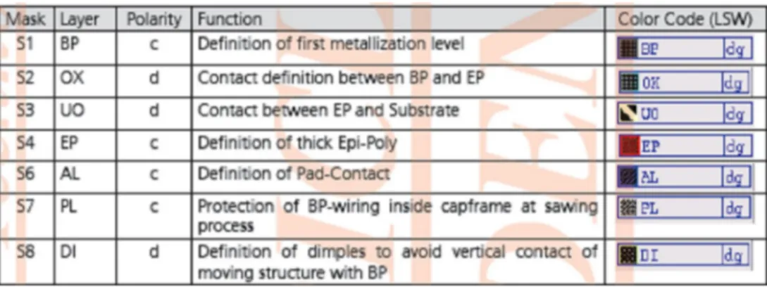
IC technology has developed rapidly during the last 50 years and the number of transistor contained within a single IC has increased following what is commonly referred as “Moore’s law” (Fig. 1).
Fig. 1 Moore’s law for integrated circuit: exponential growth in number of transistors in an IC from 1970 to 2005
Since 1970, the complexity of ICs has doubled every two to three years. The dimension of manufactured devices and ICs has decreased from 20 microns to the sub micron level of today. Current ultra large scale integration (ULSI) technology enables the fabrication of more then 10 millions transistors and capacitors on a typical chip.
IC fabrication is dependent upon sensors to provide input from the surrounding environment, just as a control system needs actuators (also referred as transducers) in order to carry out the desired outputs. Due to the availability of silicon as material (it can be produced from SiO2), a large effort was spent into
developing Silicon process and technologies to produce silicon sensors and actuators.
Attention in this area was focused on microsensors development. The first microsensor, which has been the most successful, was the silicon pressure sensor. In 1954 the piezoresistive effect in silicon and germanium was discovered [1], and many consider this discovery as the birth of MEMS. In the first decades MEMS products were limited to pressure and acceleration sensors, but in a short time they
started affecting the nation’s economy and wealth. In the 1980s and 1990s, many governments heavily funded the development of MEMS technology, particularly the United States, Japan and Germany.
A so high level of interest in MEMS technology comes from both business and technical directions. In fact they are attractive to business because multiple emerging markets for MEMS promise large financial gain and they are also attractive from a technological point of view. More in detail MEMS technical attractiveness include multiple factors:
− cost of single device scales with its size as a result of batch manufacturing technology (batch fabrication involves the simultaneously manufacturing of hundreds or thousands of identical parts thus diluting the impact of fixed costs, including the costs of maintaining expensive cleanrooms and assembly facilities);
− MEMS devices are characterized by excellent mechanical properties due to their pure crystalline structure (eliminating mechanical fatigue and hysteresis makes silicon almost a perfect material for sensors, its mechanical properties are comparable to steel);
− MEMS can be fabricated by using the same technology infrastructure already created for IC industry. This involves to have processing equipment, sophisticated diagnostic and test equipment, design and simulation tools, high volume IC packaging technologies immediately available for MEMS production;
− there is potential for the MEMS integration with IC circuitry to create low cost integrated mechanical, optical and biological systems on a chip;
− there is an available pool of educated silicon processing technologists; − MEMS can be used as a packaging vehicle for nano devices, thus
suggesting synergy with nanotechnology which receives a high level of worldwide government funding.
Even though MEMS technology has been very promising, commercialization efforts have encountered multiple stumbling blocks that have significantly delayed the availability of commercial devices. A first stumbling block was the fact that the IC industry has not provided all process modules required to fabricate mechanical devices (such as wafer deep etching, double side wafer alignment and multiple wafer bonding) and the development of such MEMS processes was long and expansive. Secondly, the mechanical properties of IC materials were unknown and dependent on the fabrication process as well as electrical stability of silicon structures. The third point is that in the IC industry the structure thickness was not an issue, IC industry required an accuracy on thickness of about ±10%, but in MEMS industry the thickness becomes a key point and a better control for mechanical thickness is required. Moreover high volume, low cost MEMS dedicated testing had to be developed entirely by the MEMS industry. And finally the compatibility with the real world was the major task to be developed by MEMS industry. All these factors have slow down the development of the first MEMS products and the volume implementation of the first devices was very slow, as shown in Tab. 1.
Product First Prototype Cum Volume 1M Incubation
Pressure sensor 1961 1984 23 years
1970 piezoresistive 1995 25 years
Acceleration sensor
1977 capacitive 1995 18 years
Ink jet printers 1977 1996 19 years
Displays 1979 2001 22 years
Tab. 1 Volume implementation of the first devices
The incubation periods shown in Tab. 1 may seem long, but they are similar to the incubation of other emerging technologies such as cell phones or satellite TV. In the 1990s, MEMS programs had been established at all major university all around the world and several hundred MEMS fabrication facilities have been founded since 2005 in academic and commercial environments.
In 2007, 2 billion MEMS units have been produced and 2.5 billion have been produced in 2008. But by 2012, it is 6.7 billion of MEMS devices which will be shipped worldwide. An interesting fact is that, despite the large 2007/2008 increase in units for MEMS (25%), the market value growth is “only” 9%. This effect is justified by a strong price pressure MEMS devices are currently subject to. After 2009, RF MEMS and Si microphones will both contribute to the largest number of MEMS devices (over 45%).
1.2.
MEMS fabrication and technologies
MEMS devices and systems involve some form of lithography-based microfabrication borrowed from the microelectronic industry and enhanced with specialized techniques generally called “micromachining”. As mentioned in the previous section, the batch fabrication, that is characteristic of microelectronics industry, offers a potential for great cost reduction when manufacturing in high volume. Micromachining is a batch process in which dozen to tens thousands of identical elements are fabricated simultaneously on the same wafer.
Lithographic techniques generally require the use of flat substrates. Silicon is often used even when there are no electronic components in the device because the tools and the instruments needed for microfabrication are designed to match the characteristics of silicon wafers.
Silicon micromachining combines adding layers of material over a silicon wafer with etching (selectively removing material) precise patterns in these layers or in the underlying substrate. The implementation is based on a broad portfolio of fabrication processes including material deposition, patterning and etching techniques (see Fig. 3). Lithography plays a key role in the definition of accurate and precise patterns and it offers in-plane sub-micron precision on dimensional scales from micron to millimetre. Thin film deposition and etching techniques in combination with wafer-bonding techniques allow patterning of the third dimension, making possible the creation of movable parts. The combination of lithography with thin-film methods tends to result in structure characterized by extrusion of two-dimensional features into the third dimension.
Fig. 3 Basic process flow in micromachining: layers are deposited; photoresist is lithographically patterned and then used as a mask to etch the underlying materials. The process is repeated until the completion of the microstructure.
From previous description is clear that microfabrication is based on planar technologies: constructing the electronic devices and MEMS components on substrates that are in the form of initially flat wafer. Starting from the silicon substrate, MEMS are fabricated using the same standard process steps used in integrated circuit manufacturing including photolithography, wet and dry etching, oxidation, diffusion, low-pressure chemical vapour deposition (LPCVD) and sputter deposition.
Common practice is to classify MEMS process flows into two primary types: bulk
micromachining and surface micromachining. Bulk micromachining encompasses
flows that etch deeply into the substrate, while surface micromachining collects flows that create microstructure with the removal of sacrificial layers from beneath thin-film structures, leaving free standing mechanical structures.
Requirements of a MEMS process flow are inclusion of one or more mechanical materials, steps process to shape these materials and, in most cases, steps process to release parts of the structural material from other anchored materials. The choice of micromachining process depends on the specifications on device dimensions and tolerances. Usually over 10µm thickness structures require bulk micromachining, while structures under 10µm incorporate surface micromachining or hybrid bulk/surface micromachining.
They are five main categories of micromechanical materials: substrate materials, surface materials, spacers, structural materials and finally active materials. The structural materials and substrate materials, which must be the same, must be able to survive to the various process steps. Spacer materials are usually completely etched or partially etched away to release microstructures and because of this function they are also called sacrificial materials. Surface materials may be used to protect the substrate or structural materials for certain etching steps, and they are also important to achieve electrical isolation. Finally active materials are incorporated on structures to exploit their special physical transduction characteristics. Probably every possible transduction mechanism has been explored in MEMS. Common transduction effects are silicon piezoresistance to measure stress, the piezoelectric effect in ZnO for both stress sensing and actuation, temperature coefficient of resistance and thermoelectric properties of silicon, aluminium and other conductors to measure temperature and various magnetic materials to couple mechanically to magnetic fields.
It is not possible to identify a single process flow which can be used to fabricate all possible MEMS devices, however some canonical process flows cover the basic MEMS fabrication concepts and form a basis for many other derivates. These canonical process flows are: silicon etching and bonding, surface micromachining and bulk micromachining.
1.2.1. Silicon etching and bonding
Silicon is one of the few materials that are economically manufactured in single crystalline substrates. This crystalline nature provides significant electrical and mechanical advantages. In fact the precise modulation of silicon electrical conductivity using impurity doping is the very core of the operation of semiconductor devices, while from a mechanical point of view it is extremely robust and stable with mechanical characteristics similar to steel.
Silicon as an element exists with three different microstructures: crystalline,
amorphous silicon are usually deposited as thin films with typical thicknesses below 5µm. Crystalline silicon substrates are commercially available as circular wafers characterized by 100-mm and 150-mm diameters, larger diameter used by the integrated circuit industry are currently economically unjustified for MEMS. Silicon has a diamond-cubic crystal structure and its crystallographic planes play an important role in the design and fabrication of silicon based MEMS and deeply affect some material properties.
Silicon etching is one of fundamental process for MEMS fabrication. In etching the objective is to selectively remove material using imaged photoresist as a masking template. The pattern can be etched directly into the silicon substrate or into a thin film, which may be in turn used as a mask for subsequent etches. For a successful etch there must be sufficient selectively between the material being etched and the masking material. Etch processes for MEMS fabrication deviate from traditional etch processes for the integrated circuit industry and remain to a large extent an art.
Several etching techniques exist, the most important for MEMS fabrication are: − wet isotropic and anisotropic etching;
− electrochemical etching; − plasma etching;
− reactive ion etching (RIE) and deep reactive ion etching (DRIE).
Wet chemical etching is widely used in semiconductor processing and it is the
oldest form of etching. It consists in the immersion of a patterned substrate in a suitable chemical liquid that attacks the exposed regions of the substrate and leaves the protected regions alone. The rate of etching and the shape of the resulted etched region depend on many factors such as the type of substrate, the specific chemistry of the etchant, the choice of the masking layer, the temperature and whether or not the solution is well stirred. Wet etching can etch very deeply in the substrate and this is the motivation because it is common to refer to these processes as bulk micromachining. Most of the wet etching processes are
isotropic, that means that are unaffected by crystallographic orientation and
consequently the rate of the material removal does not depend on substrate orientation (the most common isotropic wet etchant is HNA which is a mixture of hydrofluoric, nitric and acetic acids).
Fig. 4 Pattern transfer by isotropic wet etching through the openings in a mask layer. Because the wet etch is isotropic, the mask is undercut and the sidewall is
However some wet etchants exhibit orientation-dependent etch rate and they perform an anisotropic wet etching. Specifically strong bases such as potassium hydroxide (KOH), tetramethyl ammonium hydroxide (TMAH) and ethylene diamene pyrocatechol (EDP) exhibit preferential etching along the <100> and <110> crystallographic directions and orders of magnitude smaller etch rate in the <111> direction. Consequently a long etch of a silicon wafer with orientation <100> will determine <111> planes everywhere, as shown in Fig. 5.
Fig. 5 Anisotropically wet etched pit in <100> silicon wafer
For these kind of etchants a silicon oxide or silicon nitride mask must be used in general.
The relative large etch rates of anisotropic wet etchants (>0.5 µm/min) make it difficult to achieve uniform and controlled etch depths. Some applications, such as bulk-micromachined pressure sensors, demand a thin silicon membrane (5 to 20µm) with dimensional thickness control and uniformity better than 0.2µm, which is very hard to achieve using timed etching. Instead the thickness control is reached using a precisely grown epitaxial layer and controlling the etch reaction with an externally applied electric potential. This method is commonly referred as
electrochemical etching.
Another etching technique widely used in MEMS fabrication is the plasma etching technique. Plasma etching involves the generation of chemically reactive neutrals and ions that are accelerated under the effect of an electric field toward a target substrate. The reactive species are formed by collision of molecules in a reactant gas (e.g., SF6, CF4, Cl2, NF3) with a cloud of energetic electrons excited by a RF
electric field. When the etch process is purely chemical, powered by the spontaneous reaction of neutrals with silicon, it is colloquially referred to as plasma etching. But if ion bombardment of the silicon surface plays a synergistic role in the chemical etch reaction, the process is then referred to as reactive ion etching
(RIE).In RIE, ion (e.g., SFx+) motion toward the substrate is nearly vertical, which gives RIE vertical anisotropy. Moreover starting from 1990s the deep reactive ion
etching (DRIE) technique has been developed in order to have an etch process
capable of obtaining vertically etching high-aspect-ratio trenches.
As well as etching, bonding is another fundamental process used in MEMS fabrication and packaging. Wafer bonding is a method for firmly joining two wafers to create a stacked wafer layer. There are three types of wafer bonding techniques:
− direct bonding;
− field assisted bonding;
− bonding with an intermediated layer.
In direct bonding the first step is the cleaning of the surfaces to be bonded, then the surfaces are contacted and pressed together, using hydrogen bonding to
provide a modest degree of adhesion. Finally the contacted pair is placed in a high temperature furnace to fuse the two wafers together. The resulting bond is as strong as silicon itself. An alternative method, which is restricted to certain glasses bonded to conductors is called field assisted bonding or anodic bonding. The mechanism responsible for anodic bonding is the mobility of sodium ions in the glass. When the silicon wafer is placed on the glass, and the two are heated to temperature in order of 500°C, a positive voltage applied to the silicon repels sodium ions from the glass surface creating a negative charge at the glass surface. The attraction force between positively charged silicon wafer and the negatively charged glass surface brings the two surfaces intimate contact. Finally another common bonding technique adopted in MEMS fabrication is the bonding with an
intermediate layer. This technique is similar to the common use of adhesive to
bond structural elements together. In the case of microelectronics the adhesive elements must meet the thermal and cleanliness requirements of microfabrication and they are in general special glasses, or gold layer or polymeric adhesive. An example of MEMS processes that combines together two techniques described above is the dissolved wafer process. The dissolved wafer process combines wet silicon etching and wafer bonding to form boron doped microstructures on a glass substrate. An example of dissolved wafer process flow is shown in Fig. 6 for an inertial latch. This inertial latch closes a gold contact when exposed to threshold acceleration [3]. The “handle” silicon wafer is a sacrificial mold for defining the height of the microstructures. Thin silicon oxide layer is deposited to make electrically isolating springs as shown in Fig. 6. The front side of silicon wafer with the patterned structural layers is anodically bonded to a glass substrate with gold interconnect. The glass substrate has excellent bond strength to silicon. For capacitive sensor applications, the use of a glass eliminates capacitive parasitic that would be present if a conductive silicon substrate were used instead. The structures are released by etching the entire handle wafer with a wet silicon attach.
Fig. 6 A dissolved wafer process. (a) Masked boron diffusion. (b) Silicon oxide deposition and patterning for silicon etch. (c) Silicon etch and mask strip. (d) Silicon
oxide deposition and patterning; Chromium and gold deposition and patterning. (e) Anodic bonding. (f) Dissolve handle wafer for release.
1.2.2. Surface micromachining
Since the beginning of the 1980s much interest has been directed toward micromechanical structures fabricated by a technique called surface micromachining which is based on deposition and subsequent attach of sacrificial
layers on the silicon substrate, in order to create the MEMS components (the sacrificial material is employed during the fabrication process to realise the microstructure but does not constitute any part of the final miniature device). The main advantages of this technique are that the surface micromachined structures can be an order of magnitude smaller than the bulk micromachined ones, and can be easily integrated with integrated circuit components.
There are several approaches for surface micromachining: the first approach is the sacrificial layer technology for the realisation of microstructures, the second approach incorporates IC technology and wet anisotropic etching and finally the third approach uses plasma etching to fabricate microstructures at the silicon wafer surface.
The most widely used is the sacrificial layer approach. This technology uses in most situations polycrystalline silicon instead of single-crystal silicon as the structural material, in fact low pressure chemical vapour deposition (LPCVD) of polysilicon (poly-Si) is well known in standard IC technologies and polysilicon has excellent mechanical properties that are similar to single-crystalline silicon. When polycrystalline silicon is used as structural layer, silicon dioxide (SiO2) is usually
employed as the sacrificial material.
The principal process steps in sacrificial technology are:
− Deposition and patterning of a sacrificial SiO2 layer on the substrate.
− Deposition and definition of a poly-Si film.
− Removal of the sacrificial oxide by lateral etching in hydrofluoric acid (HF), which means etching away the oxide underneath the poly-Si structure. A typical example of surface micromachining application is the creation of a freestanding beam anchored to a silicon substrate via an insulating nitride layer (Fig. 7). A layer of silicon nitride is first deposited by LPCVD on a silicon wafer. The nitride film will be the base on which the beam will lie and it acts as a protective layer for the substrate. A layer of sacrificial SiO2 is deposed by chemical vapour
deposition (CVD) on the top of nitride layer (Fig. 7(a)) and patterned as shown in Fig. 7 (b). The thickness of the patterned oxide is equal to the distance between the final freestanding beam and the silicon nitride layer. At this point polysilicon is deposed by LPCVD on the patterned oxide as shown in Fig. 7(c) and finally the sacrificial SiO2 is laterally etched and the freestanding beam is created.
1.2.3. Bulk micromachining
Bulk micromachining is the most used of the two principal silicon micromachining technologies. It emerged in the early 1960s and has been used since then in the fabrication of many different structures. Bulk micromachining is used in the manufacture of the majority of commercial devices (almost all pressure sensors and silicon valves and 90% of silicon acceleration sensors).
The term bulk micromachining suggests the fact that this micromachining technique realizes microstructure within the bulk of a single-crystal silicon (SCS) wafer by selecting removal the wafer material.
The microstructures fabricated by using bulk micromachining may cover the thickness range from submicrons to the thickness of the full wafer (200 to 500 um) and the lateral size ranges from microns to the full diameter of a wafer (75 to 200 mm).
Etching is the key technological step for bulk micromachining, and the etching techniques used several of the aforementioned techniques:
− wet isotropic and anisotropic etching; − plasma isotropic etching;
− reactive ion etching ; − etch-stop technique.
Some of these etch processes have already been used as a standard technology in the microelectronics industry (e.g. reactive ion etching).In addition to etch process, bulk micromachining often utilises wafer bonding technology and buried oxide-layer technology.
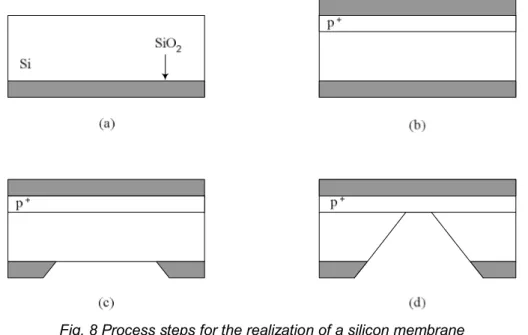
Bulk micromachining is typically used to obtain membranes used in pressure sensors. The process steps used to realize a typical membrane is shown in Fig. 8.
Fig. 8 Process steps for the realization of a silicon membrane
The starting structure is a silicon single-crystal silicon substrate with a silicon oxide layer on the inferior surface (Fig. 8 (a)). Then a Boro diffusion is realized to create an etch stop p+ doped region, and a silicon oxidelayer is grown on the upper wafer surface in order to protect the wafer surface during the etching phase (Fig. 8(b)). The third step is the creation of the mask used to obtain the desired geometry and finally the last step is the creation of the membrane by etching the silicon from the backside opening. This etch is typically performed by using KOH etchant and the attach will stop in correspondence of the p+ region.
With the structure described above piezoresistive pressure sensor can be realized by simply building polysilicon resistors on the top of the membrane [4]. Any deflection due to pressure differences between the two membrane sides will induce either compressive or tensile stress on the resistors changing slightly their resistances.
1.3.
MEMS leading applications
Microelectromechanical systems represent the outstanding state of art for a broad range of applications such as biomedical applications, communication applications, automotive, and optical applications.
Indeed micromachining and MEMS technologies can be used to produce complex electrical, mechanical, fluidic, thermal, optical and magnetic structures, devices and systems on a scale ranging from organs to subcellular organelles. This miniaturization ability has enabled MEMS to be applied in many areas of biology, medicine and biomedical engineering, a field generally referred as BioMEMS. BioMEMS research fields and applications are the most disparate: realization of microsensor arrays that act as electronic noise or tongue, microfabrication of neural systems capable of controlling motor or sensory prosthetic devices, painless microsurgical tools, complete microfluidic systems for total chemical or genetic analysys and drug delivery systems are only some examples.
In order to report some examples of BioMEMS applications we can mention the commercially successful low-cost disposable medical pressure sensor developed by Lucas NovaSensor NPC-107 [5]. The development of surgical microgrippers actuated by shape-memory-alloy forces which are capable of grasping tissues during endoscope surgical procedures [6]. And finally scalpel driven by a piezoelectric microactuator which is an innovative example of using MEMS technology in surgical tools [7]. The aforementioned devices are only few examples of BioMEMS systems, but are sufficient to show the variety and the incisiveness of MEMS applications in medical filed.
Another filed in which MEMS have shown to be a winning choice is RF applications. Indeed MEMS applications in RF and microwave electronics are revolutionizing wireless communications and promise to provide innovative applications. The term “RF MEMS” encompasses several distinct types of devices, including RF switches and relays, resonators, varactors (variable capacitors) and inductors. Applications of RF MEMS include all types of wireless communications, radar, satellites, military radio, instrumentation and test equipment. Compared to conventional RF components, RF MEMS offer significant benefits, including lower power consumption, lower insertion loss, smaller form factor and enhanced re-configurability which can result in superior functionality and performance.
RF MEMS have come to market more recently than other types of MEMS, but the RF MEMS market is now growing rapidly. RF MEMS switches can be classified by actuation method (electrostatic, magnetic, piezoelectric, thermal), by contact mechanism (capacitive, metal-to-metal), or by anchor mechanism (cantilever, fixed-fixed beam) [8]. And they are typically composed by a thin metal cantilever, a bridge, a diaphragm (or some similar structure) to open an RF transmission line or shunt it to ground. MEMS switches feature excellent RF characteristics, thus outperforming many traditional RF circuits.
Even if MEMS devices find employ in a wide range of applications, such we have seen before, the two leading MEMS applications are without any doubt automotive applications and optical applications. Then it’s important to have a more detailed description of these application fields, as will be shown in next two paragraphs.
1.3.1. MEMS for automotive applications
The automotive market has been a key driving market for the development of microelectromechanical systems.
Automotive MEMS applications began with the manifold absolute pressure sensor (MAP), developed by many companies in the mid-80s. The MAP sensor was used together with a manifold air temperature sensor (MAT) to compute the density of air entering the engine. The product of air density and engine speed gave the mass of air entering the engine, this information was used to control the engine air-to-fuel ratio thus efficiently minimizing the tailpipe emissions, and bringing them into compliance with federal regulations.
Only the non-invasive blood pressure sensor and the ink jet print head rivalled this application as the initial high-volume micro-electromechanical device. The first MAP sensor was a uncompensated bulk micromachined piezoresistive pressure sensors, then continuous progress in technology allowed improving the sensor structure and the conditioning read out electronic until having a CMOS-integrated, bulk micromachined pressure sensor with non-volatile memory allowing the incorporation of state-of-the art digital signal processing to add features like three-wire interface, changeable rail voltages, and improved accuracy [9]. Today, the volumes of MAP sensors continue to grow and are measured in millions of units per year, matching the total volume of cars and trucks produced by the automotive industry each year. Further, newer versions of these MAP sensor devices have been designed, which take advantage of the advances in the MEMS processing technology.
A similar scenario was played out in the mid-1990’s, when air-bag restraint systems were introduced. Non-MEMS, ball-in-tube acceleration sensors were used for relatively high-cost, inflatable restraint systems when these were vehicle options. When mandated, the need for a lower cost motion sensor became apparent. Micromachined accelerometers were able to fill this need, and are replacing most original sensing technologies in the automobile. Then in the 1990s the airbag-deployment accelerometer started high volume production and several companies developed capacitive accelerometer fabricated with surface micromachining technique (Fig. 9).
Fig. 9 The initial Analog Devices (left) and Motorola (right) accelerometers for airbag deployment.
Automotive applications have some stiff requirements, indeed they have to guarantee high quality and exceptional reliability in addition to low costs.
Even with the challenging requirements of the automotive market, its high volumes (15 million cars/year in the US alone), have provided incentive for continued development of MEMS automotive applications. Today’s high-end vehicles feature up to 100 different sensors among which about 30 these are now MEMS, and the percentage is forecasted to grow. The market is composed by accelerometers, gyroscopes, pressure and flow sensors. Latest applications comprise IR sensors for air quality and micro-mirrors for displays. The automotive segment is accounted for $1.6 billion, making this the second biggest opportunity after IT peripherals and inkjet print heads. By 2011 the market will top $2.2 billion, with a compound annual growth rate (CAGR) of roughly 7%.
Fig. 10 Market for Automotive MEMS sensor (source wtc-consult).
The intelligent vehicle is provided by sensors and systems for collision avoidance, accident prevention and severity reduction. The main automotive sensor applications can be classified in: active safety, passive safety, navigation and drive assistance.
Active safety
Active safety represents the most important requirement in modern vehicles. The MEMS accelerometers and gyroscopes are both sensors which can perfectly fit active safety requirements in the automotive domain.
Some examples of active systems which employ MEMS technology are the well known ABS (Anti-lock Braking System) which prevents the wheels from locking while braking, Cornering Brake Control (CBC) which performs stabilisation during partial braking whilst cornering and Traction control system (TCS) which is designed to prevent loss of traction. Furthermore sensor systems are employed in the correction of drive trajectory: Electronic (Dynamic) Stability Control (ESC, ESP) compares the driver's intended direction, to the vehicle's response, via lateral acceleration, rotation (yaw) and individual wheel speeds. ESC then brakes individual front or rear wheels and/or reduces engine power as needed to get correct under steer or over steer.
Fig. 11 Effect of ESC Passive safety
The main examples of passive safety system are the intelligent airbags. They care to soften impact for passengers during car crashes. Since the airbag system must act at the right instance and also with the proper force toward the car occupants, the identification of type of collision, collision direction, g-force impact assumes critical importance. The adoption of MEMS accelerometer, thanks to their high integration capability and accuracy, can lead to detection system of new generation replacing standard electromechanical system, achieving enhanced passenger care. Since the instant of the impact cannot be predicted in advance, it is extremely important to detect for each passenger the seat position and if at the moment in which the crash happens the occupant is lifted from the seat. The MEMS accelerometer can determine the correct positioning of car occupants to dose the force of airbags bang.
Inertial navigation system
The satellite navigation system in vehicles allows determining the position of the car anywhere on the world by radio signals from Global Positioning System (GPS) satellites. Nevertheless, data from satellite is not sufficient to constantly determine the correct positioning since the satellite signal could not be always available due to shadowing by buildings and overpasses especially in crowded urban areas. In this scenario, a dead reckoning GPS system can replace the navigation system continuing tracking movements during the time when satellite signals are not available. MEMS-based gyroscope and a magnetometer can path the motion direction and together with an accelerometer which gives information about velocity of the moving object can implement complementary tracking system to GPS. These systems are called inertial navigation systems (INS) and they can detect a change in the geographic position (a move east or north for example), in the velocity (speed and direction of the movement) and in the orientation (rotation about an axis) of a moving object.
The working principle of an INS is described in the following. MEMS gyroscopes measure the angular velocity of the system in the inertial reference frame. By using the original orientation of the system in the inertial reference frame as the initial condition and integrating the angular velocity, the system's current orientation is
known at all times. Accelerometers measure the linear acceleration of the system in the inertial reference frame, but in directions that can only be measured relative to the moving system (since the accelerometers are fixed to the system and rotate with the system, but are not aware of their own orientation). However, by tracking both the current angular velocity of the system and the current linear acceleration of the system measured relative to the moving system, it is possible to determine the linear acceleration of the system in the inertial reference frame. Performing integration on the inertial accelerations (using the original velocity as the initial conditions) using the correct kinematic equations yields the inertial velocities of the system, and integration again (using the original position as the initial condition) yields the inertial position.
Driver assistance
Driver assistance systems are systems studied to help the driver in the driving process. Some example of drive assistance systems are Adaptive Cruise Control (ACC), Intelligent Speed Adaptation (ISA), Intelligent Light Positioning, or Automatic Parking.
Adaptive or Autonomous Cruise Control (ACC) is an optional cruise control
system appearing on some more upscale vehicles. The system goes under many different trade names according to the manufacturer. These systems use either a radar or laser setup allowing the vehicle to slow when approaching another vehicle and accelerate again to the preset speed when traffic allows. ACC technology is widely regarded as a key component of any future generations of intelligent cars.
Fig. 12 Schematic of automatic cruise control (the read car automatically follow the blue car)
Intelligent Speed Adaptation (ISA), also known as Intelligent Speed Assistance,
is any system that constantly monitors vehicle speed and the local speed limit on a road and implements an action when the vehicle is detected to be exceeding the speed limit. This can be done through an advisory system, where the driver is warned, or through an intervention system where the driving systems of the vehicle are controlled automatically to reduce the vehicle’s speed.
Intelligent speed adaptation uses information about the road on which the vehicle travels to make decisions about what the correct speed should be. This information can be obtained through use of a digital maps incorporating roadway coordinates as well as data on the speed zoning for that roadway at that location, through general speed zoning information for a defined geographical area (e.g., an urban area which has a single defined speed limit), or through feature recognition technology that detects and interprets speed limit signage. ISA systems are designed to detect and alert a driver when a vehicle has entered a new speed zone, when variable speed zones are in force (e.g., variable speed limits in school
zones that apply at certain times of the day and only on certain days), and when temporary speed zones are imposed (such as speed limit changes in adverse weather or during traffic congestion, at accident scenes, or near roadworks). Many ISA systems will also provide information about locations where hazards may occur (e.g., in high pedestrian movement areas, railway level crossings or railroad grade crossings, schools, hospitals, etc.) or where enforcement actions is indicated (e.g., speed camera and red light camera locations).
The purpose of ISA is to assist the driver in keeping to the lawful speed limit at all times, particularly as they pass through different speed ‘zones’. This is particularly useful when drivers are in unfamiliar areas or when they pass through areas where variable speed limits are used. There are several types of technology currently available for determining local speed limits on a road and determining the speed of the vehicle, in particular we focus on the one which uses MEMS sensors: dead reckoning technology.
Dead reckoning (DR) uses a mechanical system linked to the vehicle’s driving assembly in order to predict the path taken by the vehicle. By measuring the rotation of the road wheels over time, a fairly precise estimation of the vehicle’s speed and distance travelled can be made. Dead reckoning requires the vehicle to begin at a known, fixed point. Then, by combining speed and distance data with factors such as the angle of the steering wheel and feedback from specialized sensors (e.g., accelerometers, flux gate compass, gyroscope) it can plot the path taken by the vehicle. By overlaying this path onto a digital map, the DR system knows approximately where the vehicle is, what the local speed limit is, and the speed at which the vehicle is travelling. The system can then use information provided by the digital map to warn of upcoming hazards or points of interest and to provide warnings if the speed limit is exceeded.
Intelligent light positioning is gaining relevance in high end cars and is
expanding down to more market segments. MEMS sensors like accelerometer and gyroscope can lead to a new generation of head lights enhancing road illumination and guaranteeing safer driving conditions. Thanks to motion detection, and assisted by GPS systems alignment of head light to various road conditions (e.g. asphalt, curves, uphill, downhill) and on vehicle condition (e.g. speed type pressure, suspensions, number of occupants).can be automatically performed.
Automatic parking is an autonomous car manoeuvring from a traffic lane into a
parking place to perform parallel parking, perpendicular or angle parking. The automatic parking aims to enhance the comfort and safety of driving in constrained environments where much attention and experience is required to steer the car. The parking manoeuvre is achieved by means of coordinated control of the steering angle and speed which takes into account the actual situation in the environment to ensure collision-free motion within the available space.
The more recently system developed for automatic parking are Intelligent Parking Assist System (IPAS), also known as the Advanced Parking Guidance System (APGS) for Lexus models in the United States.
The IPAS/APGS uses computer processors which are tied to the vehicle's (sonar warning system) feature, backup camera, and two additional forward sensors on the front side fenders. The sonar park sensors, known as "Intuitive Parking Assist" or "Lexus Park Assist", includes multiple sensors on the forward and rear bumpers which detect obstacles, allowing the vehicle to sound warnings and calculate optimum steering angles during regular parking.[10] These sensors plus the two
additional parking sensors are tied to a central computer processor, which in turn is integrated with the backup camera system to provide the driver parking information.[11]. When the sonar park sensors feature is used, the processor(s) calculate steering angle data which are displayed on the navigation/camera touchscreen along with obstacle information. The Intelligent Parking Assist System expands on this capability and is accessible when the vehicle is shifted to reverse (which automatically activates the backup camera). When in reverse, the backup camera screen features parking buttons which can be used to activate automated parking procedures. When the Intelligent Parking Assist System is activated, the central processor calculates the optimum parallel or reverse park steering angles and then interfaces with the Electric Power Steering systems of the vehicle to guide the car into the parking spot.
1.3.2. MEMS for optical (MOEMS)
Micro –Opto-ElectroMechanical systems (MOEMS) are optical MEMS, this means that they are systems involving micromachining of structures in the micro to millimetre range whose purpose is to manipulate light.
Micro-Opto-ElectroMechanical systems represent a subset of the MEMS family that has been developed since the ’90s for fibre optics telecommunication applications as consequence of the unprecedented growth of optical communications in the late 1990’s due to the growth of the internet connections. This period of speculative growth was followed in 2001-2004 by one of the most significant market crashes in history, in which many start-up companies in who experienced unprecedented growth inaugurated with great fanfare at the end of 20th century were unceremoniously shut down at the start of the 21st century. Nevertheless the new MOEMS technology born in this period has not stopped its growth but has changed its perspective.
Historically, optical MEMS have been successfully used for TV and projection systems (this is the case of TI DLPs’ technology). Following the telecom downturn, some companies have succeeded to explore several new applications that are wide spreading the use of optical MEMS. Despite the difficulties global market has encountered in the last part of the 2008 MOEMS market has increased from 2003 to 2008 with an outstanding Compound Annual Grow Rate (CAGR) of more than 30% passing from 780 million dollar in 2003 to more than 3 billion dollar in 2008. Actually the most important fields were MOEMS are employed include: display (DMD), spectrometry, barcode scanners and picoprojetcors.
Display (DMD)
Digital Micromirror Device (DMD) is a spatial light modulator developed at Texas Instruments that is the core of Digital Light Projection (DLP) projection technology, and was invented by Dr. Larry Hornbeck and Dr. William E. “Ed” Nelson in 1987. A DMD chip has on its surface several hundred thousand microscopic mirrors arranged in a rectangular array which correspond to the pixels in the image to be displayed [12]. The mirrors can be individually rotated ±10-12°, to an on or off state. In the on state, light from the projector bulb is reflected into the lens making the pixel appear bright on the screen. In the off state, the light is directed elsewhere (usually onto a heatsink), making the pixel appear dark.
To produce greyscales, the mirror is toggled on and off very quickly, and the ratio of on time to off time determines the shade produced (binary pulse-width
![Fig. 2 Global MEMS market (Yole MEMS market forecast [2])](https://thumb-eu.123doks.com/thumbv2/123dokorg/7372602.95615/20.723.99.627.466.853/fig-global-mems-market-yole-mems-market-forecast.webp)

![Fig. 23 Strain distribution at neutral stage of a microprobe study and modeled with Ansys [24]](https://thumb-eu.123doks.com/thumbv2/123dokorg/7372602.95615/51.723.171.554.537.830/strain-distribution-neutral-stage-microprobe-study-modeled-ansys.webp)