Autore:
Luca
Magnelli Firma__________
Relatori:
Prof. Bruno Neri Firma__________
Prof. Giuseppe Iannaccone Firma__________
Prof. Felice Crupi Firma__________
Subthreshold design
of ultra low-power
analog modules
Anno 2012
UNIVERSITÀ DI PISA
Scuola di Dottorato in Ingegneria “Leonardo da Vinci”
Corso di Dottorato di Ricerca in
Ingegneria dell’Informazione
(SSD: Ing-Inf-01)
Tesi di Dottorato di Ricerca
2
SOMMARIO
Il consumo di potenza rappresenta l’indicatore chiave delle performance di recenti applicazioni portatili, come dispositivi medici impiantabili o tag RFID passivi, allo scopo di aumentare, rispettivamente, i tempi di funzionamento o i range operativi. La riduzione della tensione di alimentazione si è dimostrata l’approccio migliore per ridurre il consumo di potenza dei sistemi digitali integrati. Al fine di tenere il passo con la riduzione delle tensioni di alimentazione, anche le sezioni analogiche dei sistemi mixed signal devono essere in grado di funzionare con livelli di tensione molto bassi. Di conseguenza, sono richieste nuove metodologie di progettazione analogica e configurazioni circuitali innovative in grado di lavorare con tensioni di alimentazioni bassissime, dissipando una potenza estremamente bassa. Il regime di funzionamento sottosoglia consente di ridurre notevolmente le tensioni applicabili ai dispositivi ed si contraddistingue per i livelli di corrente molto bassi, rispetto al ben noto funzionamento in forte inversione. Queste due caratteristiche sono state sfruttate nella realizzazione di moduli analogici di base ultra low voltage, low power.
Tre nuove architetture di riferimenti di tensione, che lavorano con tutti i transistor polarizzati in regime sottosoglia, sono stati fabbricati in tecnologia CMOS 0.18 μm. I tre circuiti si basano sullo stesso principio di funzionamento per compensare gli effetti della variazione della temperatura sulla tensione di riferimento generata. Tramite il principio di funzionamento proposto, la tensione di riferimento può essere approssimata con la differenza delle tensioni di soglia, a temperatura ambiente, dei transistor. Misure sperimentali sono state effettuate su set con più di 30 campioni per ogni configurazione circuitale. Una dettagliata analisi statistica ha dimostrato un consumo medio di potenza che va da pochi nano watt a poche decine di nano watt, mentre la minima tensione di alimentazione, raggiunta da una delle tre configurazioni, è di soli 0.45 V. Le tensioni di riferimento generate sono molto precise rispetto alle variazioni della temperatura e della tensione di alimentazione, infatti sono stati ottenuti coefficienti di temperatura e line sensitivity medi a partire rispettivamente da 165 ppm/°C e 0.065 %/V.
Inoltre, è stata trattata anche la progettazione di amplificatori ultra low voltage, low power. Sono state illustrate linee guida dettagliate per la progettazione di amplificatori sottosoglia e le stesse sono state applicate per la realizzazione di un amplificatore a due stadi, con compensazione di Miller, funzionante con una tensione di alimentazione di 0.5 V. I risultati sperimentali dell’op-amp proposto, fabbricato in tecnologia CMOS 0.18 μm, hanno mostrato un guadagno DC ad anello aperto di 70 dB, un prodotto banda-guadagno di 18 kHz ed un consumo di potenza di soli 75 nW. I risultati delle misure sperimentali dimostrano che gli amplificatori operazionali in sottosoglia rappresentano una soluzione molto interessante nella realizzazione di applicazioni efficienti in termini energetici per gli attuali sistemi elettronici portatili. Dal confronto con amplificatori ultra low power, low voltage presenti in letteratura, si evince che la soluzione proposta offre un miglior compromesso tra velocità, potenza dissipata e capacità di carico.
3
ABSTRACT
Power consumption is the key performance indicator of emerging portable applications such as implantable medical devices or passive RFIDs, in order to increase their battery autonomy or operating range, respectively. Supply voltage reduction has proven to be the best approach to reduce power consumption in integrated digital systems. In order to keep pace with supply voltage reduction, also analog sections of mixed signal systems should be able to operate with very low voltage levels. Therefore, innovative analog design methodologies and circuit configurations to be operated at very low supply voltages, while dissipating extremely low power, are required. Subthreshold regime allows a remarkable reduction of the supply voltages and is characterized by very low current levels, when compared to the well known strong inversion operation. Those two features have been exploited in the implementation of ultra low power, low voltage analog subsystems.
Three novel voltage reference architectures, operating with all transistors biased in weak inversion, were fabricated with a 0.18 μm CMOS technology. The three circuits are based on the same operating principle to compensate temperature variation effects on the generated voltage. By means of the proposed operating principle, the reference voltage can be approximated by the difference of transistor threshold voltages at room temperature. Measurements were carried out over sets of more than 30 samples per each circuit configuration. Detailed statistical analysis showed an average power consumption ranging from few nanowatts to few tens of nanowatts, while the minimum supply voltage, achieved by one of the three configurations, is just 0.45 V. The generated reference voltages are very accurate versus temperature and supply voltage variations, indeed, mean temperature coefficients as low as 165 ppm/°C and line sensitivities as low as 0.065 %/V were obtained.
Furthermore, the design of ultra low voltage, low power amplifier was also covered. Detailed subthreshold design guidelines of op-amps were provided and applied to the implementation of a 0.5-V two-stage Miller-compensated amplifier. Experimental results of the proposed op-amp fabricated with a 0.18 μm CMOS process showed a DC open loop gain of 70dB, a gain-bandwidth product of 18 kHz and a power dissipation of just 75 nW. Such results demonstrate that subthreshold op-amps are a very attractive solution to implement sub-1 V energy-efficient applications for modern portable electronic systems. A comparative analysis with low-voltage, low-power op-amp designs available in the literature highlighted that the proposed solution represents a better trade-off among speed, power and load capacitance.
4
INDICE
SOMMARIO ... 2 ABSTRACT ... 3 1. INTRODUCTION ... 61.1. Low-power electronics ... 6
1.2. Energy-constrained systems ... 7
1.2.1. Radio Frequency IDentification (RFID) transponders ... 7
1.2.2. Wireless Sensor Networks (WSNs) ... 9
1.2.3. Implantable medical devices ... 11
1.2.4. Ultra low-power VLSI systems ... 12
1.3. Low-power design ... 12
1.3.1. Sources of energy dissipation in VLSI CMOS circuits ... 13
1.3.2. Subthreshold CMOS circuits ... 14
1.3.3. Low-power, low-voltage analog design. ... 14
1.4. Organization of the work ... 16
2. WEAK INVERSION REGIME ... 18
2.1. Introduction ... 18
2.2. I-V characteristic ... 18
2.3. Threshold Voltage ... 22
2.4. Small signal equivalent circuit ... 23
3. LOW-VOLTAGE, LOW-POWER VOLTAGE REFERENCES ... 28
3.1. Introduction ... 28
3.2. Performance specifications ... 29
3.2.1. Line sensitivity ... 30
3.2.2. Temperature coefficient ... 30
3.2.3. Power Supply Rejection Ratio ... 30
3.2.4. Other specifications ... 30
3.3. Bandgap References (BGRs) ... 30
3.3.1. Basic principle ... 31
3.3.2. Sub-bandgap reference circuits ... 33
3.4. Subthreshold CMOS voltage references ... 37
3.4.1. BGR-principle and weak inversion ... 37
5
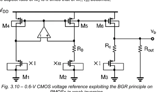
3.5. Proposed voltage references ... 45
3.5.1. Operating principle ... 45
3.5.2. Electrical configurations ... 50
3.5.3. Experimental results ... 67
4. SUBTHRESHOLD OPERATIONAL AMPLIFIER DESIGN ... 77
4.1. Introduction ... 77
4.2. Low-voltage, low-power CMOS op-amps ... 77
4.2.1. Bulk-driven MOSFETs ... 77
4.2.2. Forward body bias ... 79
4.2.3. Subthreshold operation ... 80
4.3. Design of ultra low-power, low-voltage subthreshold
opamps ... 82
4.3.1. Design guidelines ... 83
4.3.2. Two-stage op-amp design ... 87
4.4. Experimental results ... 90
CONCLUSION ... 95
6
1. INTRODUCTION
1.1. Low-power electronics
In recent years the Electronics Market has been experiencing an impressive increase in demand for battery operated equipments. Moreover, very low-power applications, like portable medical devices or microsensor nodes, represent a rapidly growing niche of such market segment. For this category of products, low power is the main requirement, and other key parameters, such as speed and/or dynamic range, might have to be sacrificed. Indeed, power consumption reduction is the most common way to extend battery lifetime, in order to reduce recharging or replacements, that are often costly and/or difficult to perform. For example, sensors for flow-rates monitoring in oil pipelines [1], sensors used in heating, ventilation and air conditioning (HVAC) systems [2] or those used to measure a building’s structural integrity during an earthquake [3], are often inaccessible and battery replacement could require infrastructure disassembling. Moreover, considering implanted medical devices, the battery replacement is not only costly but requires invasive surgery and remote charging would require high-power density that could cause tissue heating and damage [4]. Very often, in such applications, energy harvesting systems, that can further extend battery lifetime, are provided [5]. Nevertheless, power reduction issues became also crucial in applications like mobile phones and PDAs, that require high performance for limited periods of time and then spend most of the remaining time doing non-performance-critical tasks. The growing relative costs of power supplies are leading to an increasing demand for low power design techniques. In [6] the Ultra-Dynamic Voltage Scaling (UDVS) [7] was suggested as power management solution in mobile phones, since they often operate in a near-idle fashion waiting for input from the user or the wireless link. Thanks to the UDVS technique, a circuit can operate at high-voltage/high-frequency during performance-critical applications and at subthreshold/low-frequency during energy-constrained applications.
Moreover, relentless technology scaling recently gave rise to a set of reliability problems in circuits that traditionally are driven almost solely by performance constraints. These problems made power consumption an important design issue. Excessive power consumption in high performance VLSI-based systems causes self-heating, i.e. the chip temperature increases and device reliability and system performance are consequently degraded. Therefore, expensive cooling packages are required for safe operation and more and more expensive batteries are needed in order to ensure enough lifetime of high performance portable systems, such as laptops.
The growing interest towards low-power electronics is also testified by the ORTC’s (Overall Roadmap Technology Characteristics) tables [8] of the International Technology Roadmap fo Semiconductor, where specific power supply and power dissipation requirements for low-operating-power systems are specified. Moreover,
7
in the “ITRS Design and System Drivers” of the ITRS 2010 update, a key message is:
“… power consumption has become the key technical parameter that controls feasible semiconductor scaling. As a result, the device roadmap has become power-driven, and frequency is being pushed to a flat trend.”
As a consequence, energy-constrained design methodologies are gaining more and more attention in the electronic research field. Subthreshold (or weak inversion) design has become very popular nowadays in Ultra Low-Power design techniques. Although subthreshold operation was first applied more than 30 years ago to limit the power consumption of integrated circuits within electronic watches, it is recently extending to a larger market, mostly because of the relentless supply voltage scaling of integrated circuits. Indeed, supply voltage reduction is the main means for power reduction in digital circuits, leading to operate devices with voltages well below their threshold (Vth).
However, voltage downscaling and weak inversion operation pose several challenges to designers. Indeed, apart from the expected performance degradation, the most important problem they have to face is the high sensitivity to temperature variations and process variability. Moreover, considering the ever increasing need for high integration that is pushing towards mixed-signal SoCs, analog subsections are also supposed to operate, in the near future, with decreasing supply voltages, e.g. under 1 V. In that case, only few procedures for subthreshold analog design have been proposed [9].
Nevertheless, weak inversion operation allows power savings around 10x or 100x compared with strong inversion operation. In the following paragraphs a survey of applications for which energy consumption is the key performance indicator is presented.
1.2. Energy-constrained systems
1.2.1. Radio Frequency IDentification (RFID) transponders
Radio Frequency IDentification is a technology that exploits RF signals to exchange data between a reader and an electronic tag, for purpose of identification and tracking. RFID tags are relatively small and cheap. They are, usually, attached to the objects to be automatically identified. The RFID technology was originally proposed as a replacement of barcodes and smart cards whereas, nowadays, its area of application is growing increasingly: supply chain management, access control to buildings, public transportation and open-air events, airport baggage, animal identification, express parcel logistics, and many more. To meet the requirements of such applications an RFID systems must have several specific features, among them the most important are extreme low power and low cost. Identification information is stored within the silicon chip included in the RFID transponder. Therefore, it can be identified in a unique way by an identification code. Basically, the silicon chip can store a large amount of information that can be read and written wirelessly at a distance of up to several meters. Typically, tags are grouped in two main categories, depending on the presence or the absence of an autonomous power source on board. They are defined “active” if they require an on-board battery to supply all or part (in that case they are called semi-passive) of
8
the power required by the transponder for transmission and data processing. A “passive” RFID tag, instead, does not have an on-board battery, thus the transponder is supplied by rectifying the RF power transmitted by the reader. In particular, a fraction of such power is employed by the tag to communicate with the reader by modulating the impedance that the reader sees. It follows that passive devices are usually smaller and their lifetime is not limited by energy, although their available power budget is very limited.
RFID transponders design is definitely power-driven. Reducing power consumption would benefit both types of tags. For active tags, minimizing the power dissipation leads to longer battery lifetimes. For passive tags, instead, the power is constrained by the ability to utilize the converted energy from the built-in antenna. If the power dissipation can be reduced, then the distance between the reader and the tag can increase since less transmitted power has to reach the tag. As an example of an RFID transponder architecture, the one of the passive transponder IC fabricated in [10] is shown in Fig. 1.1,
The nature of the antenna varies accordingly to the coupling method adopted in the RFID system. In the case of inductive coupling the antenna is a coil, inductive coupling systems operate at frequencies around 135 kHz or 13.56 MHz achieving operating ranges smaller than 1 m. In electromagnetic coupled RFID systems, the coupling element is an antenna, which typically is a dipole or a patch antenna. They usually exploit an electromagnetic coupling in the UHF (868 MHz in Europe and 916 MHz in USA) or wave range (2.45 GHz or 5.8 GHz). Such systems can reach an operating range of few meters, in the case of passive transponder, and larger than 15 m, in the case of active transponder. The voltage multiplier converts a part of the incoming RF signal power to DC for a voltage regulator (e.g. [11]) which provide a stable power supply for all active circuits on the chip. The average input impedance of the voltage multiplier should be power matched with the antenna in order to reduce losses. The demodulator converts the pulse-width-modulated input signal to digital data and generates a synchronous system clock. The control logic handles the received data that can be written or read. A charge pump circuit is provided to obtain suitable voltage levels for EEPROM programming. The modulator then converts data from the control logic to changes in the input impedance using a MOS varactor.. The logic circuitry handles the protocol, including anticollision features, cyclic redundancy checks (CRC) checks,
9
error handling, enabling and disabling of analog circuits (power down, standby, power up), etc..
Further improvements in RFID systems in order to increase the operating range and/or battery lifetime can be achieved both at system level, e.g. by a proper choice of modulation technique, and at circuit level, by developing extreme low voltage, low power design methodologies.
1.2.2. Wireless Sensor Networks (WSNs)
A WSN consists of a large number (from tens to thousands) of spatially distributed autonomous sensors (nodes) that monitor physical quantities and/or environmental conditions, like temperature, sound, acceleration, vibration and strain, pressure, pollutants, etc., and cooperatively through the network to a main location. Such sensors have existed for decades but they have never been widely deployed as in recent years, because they needed wires to provide power and carry data. Nowadays, thanks to the miniaturization of electronics and improvements in battery and radio technology, each node in a WSN is self powered (i.e. battery operated) and can share the collected and/or processed information through the a series of wireless links between nodes. Specific features of interest to the end-user can be extracted from the collection of data gathered by several nodes.
First applications of WSNs were proposed in the military field, such as battlefield surveillance. Today more civilian applications are envisaged ranging from industrial to consumer applications such as: environment and habitat monitoring, industrial process monitoring and control, healthcare applications, home automation, traffic control, structural monitoring and automotive sensing.
In [12] a survey of WSNs for structural monitoring is presented, evidencing how wireless sensors can be added to existing structures much more easily, quickly and cheaply than wired sensors. A network of 64 wireless sensors has been installed on the Golden Gate Bridge in San Francisco to monitor vibrations. In the anchorage chamber of the Humber Bridge in East Yorkshire (England), humidity sensors helped maintenance, since steel struts must be kept dry. A straightforward example of how WSNs works in structural monitoring in constructions like buildings, tunnels or bridges, can be found in Fig. 1.2 ([12]).
Getting WSNs to work reliably and for a long time in similar environments presents several challenges. Generally, wireless sensors benefit from long device lifetimes, reduced costs and small size. Low power and energy harvesting from the environment increase the time before energy stored on-sensor is depleted. Performance requirements of sensor nodes are quite low, the rate at which data change, for example, for environmental or health monitoring, is of the order or seconds to minutes.
The block diagram of a wireless sensor [13] is shown in Fig. 1.3, where power consumption is the key parameter of each component. The analog front end interfaces the sensors (of temperature, pressure, humidity, etc.) with the internal blocks. Usually this first stage consists of an LNA providing adequate gain and drive strength for subsequent circuits while maintaining a high SNR. The low output rates of sensors allowed ultra low power amplifier design with devices operated in weak inversion. In [14] a 3.5 W LNA for amplifying low frequency (<300 Hz) electroencephalographic signals from electrodes placed on the scalp, is presented. After the amplification stage the sensor signals can be converted to digital,
10
Fig. 1.2 – Example of WSNs for structural monitoring
11
so they can be processed, stored and transmitted. Microwatts successive approximations register (SAR) ADCs have been designed for sensor environments [15], [16]. Voltage scaling is the most effective way of reducing energy consumption in processors as well as in memories. Notwithstanding, designers must face to increased latency and susceptibility to process variations that, for example, are much more critical in subthreshold operated devices than in those operated in strong inversion. Wireless communication is achieved by means of RF transmission. Nowadays, even the most energy efficient transceiver standards in commerce, i.e. ZigBee, WiFi or Bluetooth, have power consumptions in the order of tens of mW that is not acceptable for a typical wireless sensor. Again, due to low bandwidth, weak inversion operation and voltage scaling can help to dramatically reduce power consumption as in the case of the 0.5 V receiver presented in [17]. Network nodes require supply voltage ranging from 400 mV (for subthreshold operated modules) to 1.2 V (transmission modules). Since Lithium (3.3 V – 4.2 V), zinc-air (1.5 V) and alkaline (1.5 V) batteries are very common, dc-to-dc converting power electronics are needed. Linear regulators are often employed to create an output supply in ultra low-power applications [11]. Linear regulators buffer the output of a voltage reference that, generally, consists of a Bandgap Reference (BGR). Unfortunately BGRs tend to have W power consumption that could exceed the power budget of low-power sensor nodes. Nevertheless, CMOS voltage reference circuits with nA current levels and sub-1 V supply voltages have been developed [18], [19]. Switched capacitor networks or buck down-converters might also be used, compared to linear regulators they offer better power efficiencies but are noisier, unless the switching frequency of the network is very high. Finally, energy-harvesting systems, such as photovoltaic solar diodes or thermocouples, can be employed to recharge batteries for longer sensor lifetime. It follows that each component of the architecture should be designed to achieve robust ultra low power operation in order to allow long battery lifetime (e.g. > 1 year).
1.2.3. Implantable medical devices
Implanted Medical Devices (IMDs) are an emerging class of medical devices for continuously measuring internal health status and physiological signals [20]. Generally their purpose is to constantly monitor health parameters impossible to
12
monitor externally, like intraocular pressure in glaucoma patients [21]. Others IMDs uses the collected measurements as trigger for physiological interventions that prevent impending adverse events (e.g. epileptic seizures [22]) and for physical assistance (e.g. brain-controlled motor prosthetics [23]). The latter is also the case of the well known systems for arrhythmias detection and heartbeat correction, such as peacemakers and Implanted Cardioverter Defribillators.
Given their implantable nature these devices face severe size constraints and need to communicate and receive power wirelessly. Moreover, power consumption reduction is also crucial: early hearing aid systems dissipated few tens of mW [24], nowadays the power budget of an IMD does not exceed 500 nW [13] as in the case of the intraocular pressure monitoring sensor [13], shown in Fig. 1.4, assembled with energy harvesting elements and an RF antenna for data transmission.
Thus it is evident that IMDs are another compelling platform showing the need for innovative low-energy techniques in order to extend battery lifetime, thus reducing interventions for their replacement.
1.2.4. Ultra low-power VLSI systems
Most portable electronics used for consumer applications require a low power DSP or MCU. In that case adequate performance during active functioning is as important as low power consumption. In a variety of applications, for example, the Texas Instruments (TI) MSP430 family has been used for portable measurement, metering and instrumentation. Such MCU has a current consumption in active mode of 330 A at 1 MHz with a 2.2 V supply voltage, while in standby mode it only dissipates 1.1 A. It has been used in the SHIMMER wearable sensor platform [25] along with a CC2420 IEEE 802.15.4 radio, a triaxial accelerometer and a rechargeable Li-polymer battery. The total device power budget is 60 mW when active and a few W in sleep mode, whereas the device lifetime varies from hours to days, depending on the application duty cycle.
There are many other applications that take advantage of a wide range of performance needs to reduce energy consumption and extend the system lifetime (mobile phones, PDAs, laptops, etc.). They should minimize energy when in standby or sleep modes and maximize performance when in high activity modes. Ultra low power techniques, many of them based on the subthreshold operation mode, are also used in such applications [7].
1.3. Low-power design
Even though with the advent of the transistor and, later on, the coming of the integrated circuits, greater emphasis was placed on performance and miniaturization issues, nonetheless power dissipation was not completely ignored. Actually, battery operated equipments, such as pocket calculators, implantable peacemakers, hearing aids and, most importantly, wristwatches, drove low power electronics. As a consequence, power requirements become one of the most critical concerns in the evolution of microelectronic technology. In order to continue to improve the performance and to integrate more and more functionalities within chips, feature size had to shrink accordingly. As a result, the magnitude of power per unit area has kept growing and the associated problem of heat removal and cooling has kept getting worse. Even with the scaling down of supply voltage,
13
power dissipation has not decreased since higher levels of integration also allows for more functionalities. Moreover, in the last years, energy-constrained applications, like those shown in the previous paragraphs, have been emerging which require new design techniques to achieve longer lifetimes.
1.3.1. Sources of energy dissipation in VLSI CMOS circuits
As long as power consumption of VLSI systems is concerned, it is well known that the largest part is due to digital sections. The power consumption in digital VLSI circuits can be written as [26], [27]:
2
L DD SC DD leak DD
P
fC V
I V
I V
, (1.1)where the first addend accounts for the switching power, the second one for the short circuit power and the last one for the static leakage power. In (1.1) VDD is the
supply voltage, CL is the load capacitance, f is the switching frequency, is the
switching activity (i.e. the fraction of f representing the commutations in which energy is absorbed from the power supply), ISC is the short circuit current and Ileak is
the static leakage current.
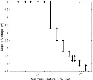
The switching power and the short circuit power form the dynamic power fraction of power dissipation in digital circuits. Thus far, the successful approach for reducing energy consumption has been VDD-scaling. Such approach has been also driven by
reliability and technological issues associated to feature size scaling as depicted in Fig. 1.5 [26],
To preserve performance and, therefore, sufficient MOSFETs’ current drive, threshold voltages (Vth) has been consequently decreased. Unfortunately Vth-scaling leads to a leakage current (Ileak) increase. In particular, decreasing VDD
and Vth, among all the leakage factors within a MOSFET [27] (pn-junction and
punchthrough leakage, gate oxide leakage, hot-carrier injection, subthreshold leakage, gate induced drain leakage, etc.), the subthreshold current becomes the prevailing one, since it changes exponentially with Vth variations.
14
Several design techniques have been developed to face with dynamic and static energy dissipation: device sizing for power efficiency [28], multithreshold design techniques [29], power gating, variable body biasing [30], [31] and subthreshold design [7], [32].
Process technology has a large effect on energy consumption of analog and digital circuits. Newer processes have smaller device capacitances and lower dynamic energy, while older technologies exhibit lower standby power (higher Vths). CMOS
processes could be optimized specifically for low power operation modes, such as subthreshold or near-threshold. For example, recent CMOS technologies include halo implants at the edge of the conducting channel to reduce the effect of the drain-induced barrier lowering (DIBL). For subthreshold operation, DIBL is not a relevant issue since the involved drain-to-source voltages are low. This, therefore, allows the removal of halo implants, which improves subthreshold swing and overall subthreshold device performance [33].
1.3.2. Subthreshold CMOS circuits
Subthreshold circuits are ideal for application where performance is not critical but minimizing energy consumption is the key. The very first employment of subthreshold conduction in the CMOS technology (1954) was inside electronic watches [34], because they needed micropower level to limit power consumption. Subsequently, in 1972, a model for subthreshold conduction was proposed in [35], in which the authors showed how applying it to find the transfer characteristic of an inverter, CMOS logic circuits can operate at a VDD as low as 8kBT/q (i.e. about
200 mV at room temperature).
At that time most subthreshold circuit design were focused on analog circuits, in [36] Vittoz and Fellrath demonstrated subthreshold circuits such as an amplitude detector, a quartz ring oscillator, a bandpass amplifier and a Proportional To Absolute Temperature (PTAT) current reference that represented the starting point of the well known Oguey’s current reference [37] capable to supply a stable current as low as 1 nA. Subthreshold transconductance amplifiers were designed for cochlea applications [38].
Subthreshold digital circuits appeared later, with the newly recognized need of limiting power consumption [39], in particular inside portable systems. With modern submicron processes, a clock frequency beyond 10 MHz can be achieved with
VDDs of just few hundred millivolts, dramatically reducing the power-delay product
[40].
As a result, the reduction of supply voltages imposed by the process of scaling down feature size imposes a reduction of the saturation voltage of transistors used in analog circuits. This is only possible to achieve by reducing the amount of MOSFET channel inversion, thus entering in weak inversion region for VDD0.5 V. 1.3.3. Low-power, low-voltage analog design.
Even though power consumption in digital circuits is dramatically reduced by voltage-scaling, low power approaches are quite different in the analog domain. Indeed, power consumption is mainly set by the required Signal-to-Noise-Ratio (SNR) and the required bandwidth in analog circuits, while decreasing VDD does not
necessarily reduce it. In analog signal processing, power is absorbed from power supply to keep the signal energy well above the fundamental thermal noise, in order to achieve a satisfactory SNR.
15
As a clarifying example let us consider the power consumed to realize a single pole characterized by the integrator shown in Fig. 1.6 [41]. The integrator consists of an integrating capacitor and a 100% efficient current transconductor (i.e. all the current absorbed from the power supply is employed to charge the capacitor). The power absorbed from the supply voltage VDD by the integrator to have a sinusoidal
voltage V(t) with a peak-to-peak amplitude Vpp and a frequency f across the
capacitor C, is 2
pp DD pp
P fCV V V . Since the output noise power is kBT/C, where kB is the Boltzmann constant and T is the absolute temperature, the SNR can be
expressed as, 2
8
pp BV
SNR
K T C
. (1.2)Therefore, the power necessary to realize a single pole, in order to fulfill a given SNR, is,
8
B B ppV
P
k Tf
SNR
V
. (1.3)As a result, the minimum power consumption at a specific T, is fixed by the SNR and the required bandwidth. It is clear that power efficient analog circuits should thus be designed to maximize the voltage swing and therefore should handle rail-to-rail signal voltages (i.e. Vpp=VDD). This power limit is very severe, since it
requires an increase of 10x in power for every 10 dB of SNR improvement. It follows that analog circuits become power inefficient in the case of systems requiring high values of SNR.
Moreover, practical circuits present further technological limitations that hinder the achievement of the discussed theoretical minimum power consumption. For example, bias circuitry (voltage and current references, current mirror, etc.) wastes energy, they should be designed in order to reduce as much as possible power consumption. Furthermore, they can increase the noise and therefore a proportional increase of power to maintain a given SNR. Since minimum power consumption is achieved for Vpp=VDD, the signal should be amplified at the early
stages of the analog systems and maintained along the processing path. Additional noise sources coming from active and passive components or from the power supply push the power to increase. Another aspect that leads to an increase in power consumption is the need for precision, which imposes the use of larger
16
dimensions for active and passive components, with a resulting increase in parasitic capacitances and, therefore, power.
Even though the minimum power consumption for a given SNR from (1.3) yields to no fundamental reasons to reduce the supply voltage, because of the technological limits described above, the power dissipated in analog circuits also depends on the
VDD value. Moreover, nowadays the trend in CMOS technologies is the VDD-scaling:
in [8] the supply voltages of low operating power systems are expected to reach 0.6 V within 2021. Furthermore, in order to avoid power consuming voltage boosting circuits, such as charge pumps, analog circuits within mixed-signal SoCs should be redesigned for ultra low-voltage.
In micropower analog circuits, MOSFETs operated in weak inversion regime provide several advantages for low-power and low-voltage purposes. The most important aspect for low-voltage systems is that the drain-source saturation voltage in weak inversion is much smaller than the one needed in strong inversion, since it is sufficient that it is larger than some thermal voltages, as will be explained in the following chapter. Moreover, another advantage strongly related to the analog design is that the transconductance-to-current ratio reaches its maximum in weak inversion. Nevertheless, weak inversion operation has drawbacks too, such as the intrinsic slowness (the transition frequency of subthreshold devices does not exceed few hundred MHz) and the higher sensitivity to process and temperature variations, compared to the strong inversion operation.
1.4. Organization of the work
In this chapter the motivations for innovative design approaches in future energy-constrained applications have been discussed. In particular, portable applications have stringent power requirements. Nowadays, one way to extend battery lifetimes is to run at microwatt power levels. Supply voltage reduction has been proved as the best approach to reduce power consumption in digital systems. In order to keep the pace with supply voltage reduction, analog sections of mixed signal systems should be able to operate with very low voltage. Moreover their power consumption should not represent the overwhelming part of the total energy budget. Therefore, novel analog design methodologies and circuit configurations to be included in battery-operated applications, where power consumption is the key performance indicator, are required. Subthreshold operation holds the most promise for ultra low power, low voltage design in analog as well as in digital domain.
In Chapter 2, subthreshold conduction in MOSFETs is examined: basic DC relations and AC small signal equivalent circuit parameters are given and discussed. Moreover a brief introduction to the EKV model is mentioned.
Chapter 3 concerns low voltage, low power voltage reference circuits. After illustrating the performance specifications of such circuits, the basic bandgap principle for temperature compensation is presented and low voltage BGR circuits are shown. Since the VGS of MOSFETs in weak inversion region exhibits a thermal
behavior (CTAT) similar to those of BJTs’ VBE, several voltage reference
architectures exploiting subthreshold operating MOSFETs have been proposed in the scientific literature. Furthermore, CMOS voltage references based on different temperature compensation techniques are also shown. Subthreshold operation
17
allowed them to work with sub-microwatt power consumption and sub-1-V supply voltages.
Subsequently, in the same chapter, the proposed voltage reference configurations are presented and discussed. They exploit an innovative temperature compensation principle based on the subthreshold operation of MOSFETs. Three electrical configurations have been implemented and fabricated in a 0.18 μm CMOS process. A detailed statistical analysis of the measurement results carried out over sets of almost 40 samples for each voltage reference architecture, is reported. Moreover, the measured performance of the best solution proposed, in terms of power consumption, minimum supply voltage and accuracy, are compared with those of low voltage, low power competitors.
Finally, Chapter 4 deals with the design of low power, low voltage op-amps. Ultra low voltage solutions exploiting techniques such as bulk-driven MOSFETs, forward body biasing and weak inversion operation are shown. The design guidelines of subthreshold op-amps are given and a design example of a two-stage Miller compensated op-amp working with just 0.5 V is presented and compared with other low power, low voltage CMOS op-amps.
18
2.
WEAK INVERSION REGIME
2.1. Introduction
The state of weak inversion (or subthreshold conduction) at the silicon surface in a metal-oxide-silcon (MOS) structure is characterized by the fact that majority carriers have been pushed away from the silicon surface, thus leaving a depletion charge of fixed atoms. The density of minority carriers is increased with respect to the distant bulk, but it is still negligible in the overall charge balance, and does therefore not affect the capacitance-voltage curves of the MOS diode. However, these minority carriers represent the only mobile charge available at the surface. Hence, as soon as some voltage is applied between the source (S) and the drain (D) of a MOS transistor structure (see Fig. 2.1), they move by diffusion, unlike strong inversion, in which the drift current dominates.
In the following the subthreshold regime in MOSFETs is described and basic expressions for the design of the ultra low-voltage low-power circuits presented in the next chapters are shown. Therefore, particular attention has been given to the impact of the subthreshold operation in analog design.
2.2. I-V characteristic
Depending on the voltages applied to the four terminals (Source-S, Gate-G, Drain-D and Body-B) the transistor can be biased in one of the three regions shown in Fig. 2.2. For gate-to-source voltages (VGSs) higher than Vth (i.e. strong
inversion region), the MOSFET operates in saturation or linear region if the drain-to-source (VDS) voltage is higher or lower than the overdrive voltage
(VOV=VGS-Vth), respectively. Subthreshold conduction is established when VGS<Vth.
The effects of the body terminal have been neglected in such description since it affects channel conduction in a similar way as the gate terminal through
Vth-variations (frequently it is also identified as second gate or backgate). Fig. 2.1 – n-channel MOSFET structure
19
When VGS is lower than Vth, the drain current does not abruptly approach zero but
follows an exponential dependence on VGS (Fig. 2.3). Fig. 2.3 also highlights the
dominant component of the channel current, i.e. the diffusion component in weak inversion and the drift component in strong inversion [42]. The transition region between the previous ones is also called moderate inversion region, where drift and diffusion currents are both significant.
The source-channel-drain area forms two back to back pn diodes, they are usually reversely biased to isolate drain and source wells from the substrate. The band profile within the channel for VGS=VDS=0 V is shown in Fig. 2.4 (a) [43]. Obviously,
Fig. 2.2 – MOSFET operating regions
0.0 0.4 0.8 1.2 10-4 10-2 100 102 Vth Strong inversion (drift) Weak inversion (diffusion)
I
D(
A)
V
GS(V)
20
in that case the net flux of charge through the channel is null. However, a VDS
increase will entirely drop across the drain-body junction, reverse biasing it more than the source-body junction, thus leading to a net current flux into the channel, Fig. 2.4 (b). Moreover, as VGS increases, a fraction of it falls across the gate oxide
while the remaining fraction lowers the potential barrier, i.e. increases the silicon surface potential S. Variation of VGS are shared between the oxide capacitance
per unit area COX and the semiconductor total surface capacitance per unit area CS
[36],
1
S OX GS OX SC
V
C
C
m
, (2.1)where m is the subthreshold slope parameter. CS can be approximated with the
depletion layer capacitance, Cd=Si/Wd where Si is the Si dielectric constant and Wd
is the depletion layer width. Given that COX=OX/tOX, where OX is the gate oxide
dielectric constant and tOX is the oxide thickness, and Si/OX3, therefore m can be
rewritten as,
3
3
2
1
d1
Si S OX OX chW
m
t
t
qN
, (2.2)in which q is the elementary charge and Nch is the channel doping concentration. In
[42] a theoretical estimation of m, considering the Wd value at the onset of strong
inversion, is given: it typically lies between 1.1 and 1.6.
The well known expression for subthreshold conduction, which also takes into account the VGS and VDS effects discussed, is [46],
(a) (b)
Fig. 2.4 – Band diagram of the longitudinal cross section of a NMOS for different values ofVDS.
21 0
1
GS th OFF DS T T V V V V mV V DW
I
I e
e
L
, (2.3) 2 0 02
Si ch T Sq N
I
V
, (2.4) where W/L is the aspect ratio of the transistor (W and L are the channel width andlength, respectively), VT=kBT/q is the thermal voltage (kB is the Boltzmann constant
and T is the absolute temperature), I0 is a characteristic current, it depends on
temperature and mobility (0) as indicated in (2.4), and VOFF is the offset voltage, it
determines the drain current at VGS=0 V.
Similarly to a bipolar transistor, ID changes exponentially with the control voltage VGS. The exponential term in round brackets takes into account the change in
current due to the reverse biasing of the drain-body junction. However, it is clear that, if VDS3÷4VT (75÷100 mV at room temperature), VDS effect on ID becomes
negligible with respect to the current coming from the source, and the subthreshold biased MOS transistor behaves as a VGS-controlled current source, as shown in
Fig. 2.5. Generally, the exponential dependence of ID on VGS represents a figure of
merit of MOSFETs, the subthreshold slope S. It specifies the required VGS reduction
to obtain an ID decrease of a factor 10,
1 10log
2.3
D T GSd
I
S
V m
dV
, (2.5) 0.0 0.4 0.8 1.2 0 1 2 3I
D(nA
)
V
DS(V)
VGS=50÷150 mV22
According to the possible variations of m, S can assume values in the range
60÷100 mV/decade.
Moreover, the drain current also depends on VDS and the body-to-source voltage
(VBS) mainly because of Drain Induced Barrier Lowering (DIBL) and body effects,
respectively. Such dependence of ID on VDS and VBS can be taken into account by
considering the following expression for Vth [45],
0
th th D DS B BS
V
V
V
V
, (2.6)in which Vth0 is the threshold voltage at room temperature extrapolated for VBS=0V, λDand λB are the DIBL effect coefficient and the body effect coefficient, respectively.
2.3. Threshold Voltage
The threshold voltage is the most critical device parameter in subthreshold design. Its variation from the expected value affects exponentially the transistor ID, unlike
strong inversion region where its influence is quadratic or linear. Primarily, Vth
deviations are due to temperature and process variations.
In a MOS system (p-type semiconductor), Vth is the voltage applied between the
metal and the semiconductor at which the electron concentration at the semiconductor surface (i.e. the conducting channel) equals the hole concentration in the bulk semiconductor, that is when S reaches the strong inversion value
2B=VTln(Nch/ni) (ni is the intrinsic carrier density). Indicating with QD the charge per
unit area stored in the depletion region, at the onset of strong inversion and with Vfb
the flat band voltage to align the gate potential and the body potential, Vth can be
written as [42],
4
2
2
g OX Si ch B D th fb B B OX OX OXE
Q
qN
Q
V
V
C
q C
C
, (2.7)where Eg is the energy bandgap of the semiconductor and QOX the equivalent
charge per unit area stored at the interface oxide-semiconductor.
Process variations affect the absolute (among different dies) and relative (within the same die) Vth precision. Apart from the relative uncertainties, that can be
reduced by means of careful circuit layout techniques, Die-to-Die variations, that cause Vth dispersion because of changes in parameters such as QOX, Nch and B,
are difficult to compensate and commonly represent the main cause of inaccuracy in analog circuits [19].
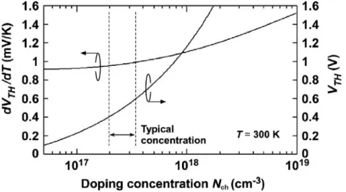
Temperature has a remarkable influence on Vth too, mainly through Eg and B
variations,
4
2.73 10 eV/°K for Si near 300°K
ln
g ch B T iE
T
N
V
T
T
n
, (2.8)23
Since ni(T) in Si increases exponentially with temperature for T>300 °K, B also
decreases when temperature increases. For example, considering a process with
Nch1016 cm-3 and m=1.1, Vth/T=1 mV/°K, that is a ΔVth=150 mV in a temperature
range -25÷125 °C, very common in modern CMOS technologies.
Although subthreshold operation offers several advantages in the ultra low-power, low-voltage scenario, it also poses challenges for the designers to devise and employ circuit compensation techniques.
2.4. Small signal equivalent circuit
In order to start a low power low voltage analog design activity with circuits employing subthreshold operated transistors a good understanding of DC parameters, frequency response and noise performances of MOSFET in subthreshold region is needed. Moreover, in this paragraph a comparison between the behavior of saturated MOSFETs in weak (VDS>3÷4VT) and strong inversion is
presented.
To this aim, the small-signal equivalent MOSFET model shown in Fig. 2.6 is considered. In the model, gm is the transconductance, rd is the drain-source
resistance, gmb is the substrate transconductance. Cgs, Cgd, Cgb, Csb, Cdb are the
gate-to-source, gate-to-drain, gate-to-bulk, source-to-bulk and drain-to-bulk capacitances, respectively. Aiming to calculate the small-signal MOSFET parameters (gm, rdandgmb), ID can be conveniently rewritten as follows according to
(2.3) and (2.6), considering a VDS>3÷4VT, i.e. neglecting the term in round brackets
in (2.3): 0 0 GS D DS B BS T T T th OFF T V V V mV mV mV D V V mV
I
e
e
e
W
I e
L
, (2.9)From (2.9), gm, rd, gmb and the intrinsic MOSFET DC gain (AV0= gmrd ) can be
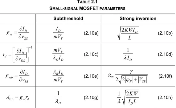
derived as reported in TABLE 2.1. The table also summarizes the values of gm, rd, gmb and AV0 in saturation region (in the expressions shown in the table, K=μnCOX is
the process transconductance and λ is the channel length modulation coefficient).
In subthreshold regime gm linearly depends on ID, while it increase with
I
D insaturation region. This leads to a greater gm/ID ratio in subthreshold than in D B S G D G B S gmvgs rd gmbvbs Cgs Cgd Cdb Csb Cgb
24
TABLE 2.1
SMALL-SIGNAL MOSFET PARAMETERS
Subthreshold Strong inversion
D m GS
I
g
v
DTI
mV
(2.10a)2
KWI
DL
(2.10b) 1 D d DSI
r
v
T D DmV
I
(2.10c)1
DI
(2.10d) D mb BSI
g
v
B DTI
mV
(2.10e)2 2
m F SBg
V
(2.10f) 0 V m dA
g r
1
D
(2.10g)
1 2
I L
KW
D (2.10h)saturation region or, similarly, the gm value is greater in a subthreshold biased
MOSFET for a fixed ID (see Fig. 2.7 [44]). Another important difference between
weak and strong inversion operation is related to the intrinsic MOSFET DC gain. In saturation region, AV0 depends on the drain current, the transistor aspect ratio, the
process transconductance and the channel length modulation parameter , whereas it only depends on the DIBL effect coefficient D in subthreshold region
25
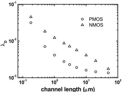
(TABLE 2.1). Since DIBL effect is strongly related to the distance between drain and
source wells, D (and consequently AV0) is mainly controlled by MOSFET channel
length. In order to have a first estimation of the minimum transistor lengths required to achieve a desired DC gain, the D-L characteristic shown in Fig. 2.8 was
extracted for the technology UMC RF/MIXED-MODE 0.18 μm. To this aim, 1 , , BS GS DS D T D D GS DS V V V
I
mV I
V
V
was derived from (2.10c), where the subthresholdslope parameter was evaluated as
, , BS DS GS GS D GS T D V V V
V
I
m
V V I
, from (2.10a). The λDand m values were extracted from SPECTRE simulations for devices with W=10
µm, L= 2 µm biased at VBS=0 V and VGS=VDS=200 mV. It is worth noting that the
threshold voltages of the CMOS process considered are 320 mV and 456 mV for NMOS and PMOS transistors, respectively.
To have a quantitative idea of dynamic performances of subthreshold operated MOSFETs, the intrinsic transition frequency fTi is considered.
1
2
2
1
2
3 2
2
d OX D T d OX m Ti X D OXC
C
I
mV WL C C
g
f
C
KWI
L
WL C
, weak inversion
=
, strong inversion
, (2.11) 10-1 100 101 102 10-3 10-2 10-1 PMOS NMOS
Dchannel length (m)
26
In (2.11) the generic expressions for the fTi of saturated MOSFET in weak and
strong inversion are given [43], where CX is the gate input capacitance
(CX=CGS+CGD+CGB(Fig. 2)). The values of CX in subthreshold (CXSUB) and strong
inversion (CXSAT) regions are given by [43],
2
2
3
3
d OX d OX X SUB GSO GDOd OX d OX
X SAT GSO GDO OX OX
C C
C C
C
C
C
WL
WL
C
C
C
C
C
C
C
WLC
WLC
, (2.12)where CGSO and CGDO are the gate-source and gate-drain overlap capacitances,
respectively, and Cd is the depletion region capacitance between gate and body
per unit area. It follows CXSUB=1.5 CXSAT at the most (for Cd→∞).
From the comparison between fTis in weak and strong inversion regions it clearly
follows that, because of the different gm/ID ratios in the two regions, fTi linearly
depends on ID in subthreshold, whereas it depends on
I
D in strong inversion. Asit appears from (2.11), the transistor speed is strongly degraded by the channel area (WL) in both operating regions. Therefore, considering the correlation
between AV0 and L in weak inversion, a trade-off should occur in the choice of
transistors channel length.
Finally, the noise performances are considered. In subthreshold region, the MOSFET drain current exhibits a white noise part (Siw=2qID) caused by shot noise
[43]. The power spectral density of the input-referred noise voltage is given by the following expressions,
2 2 22
2
8
8
3
3
2
D T m D iw vw m B B m DqI
q
mV
g
I
S
S
g
k T
k T
L
g
KWI
, weak inversion
=
, strong inversion
, (2.13)As shown, Svw depends on 1/ID and 1
I
D in weak and strong inversion regions,respectively. However, considering a single MOSFET, the output noise voltage amplitude is given by the product of the drain noise current amplitude (iDn_flicker) and
the output resistance (rD). At low frequencies iDn_flicker (
A
Hz
) in subthresholdregime is proportional to the drain current level (ID) while the output resistance (rD)
of a MOSFET is proportional to 1/ID. Therefore the low current level does not
intrinsically increases the low frequency noise. At high frequencies the shot noise current is proportional to
I
D , in that case reducing ID the output noise voltagewill increase with
I
D . However at high frequencies it becomes easy to filter noise effects.From the above discussion it results that owing to the different gm/ID behavior in the
trade-27
off among frequency response, noise performances and bias current of transistors compared with strong inversion.
28
3. LOW-VOLTAGE,
LOW-POWER VOLTAGE REFERENCES
3.1. Introduction
Ultra low power, low voltage design requirements are crucial in emerging applications such as portable medical devices, microsensor nodes and passive RFIDs. For such portable systems, power consumption reduction becomes essential to extend the battery lifetime and/or the communication range. This leads to a strong demand for circuit building blocks operating with low supply voltages and low power consumption.
Among them, Voltage Reference circuits are ubiquitous, they are broadly used in analog and digital systems to generate a DC voltage independent of Process, supply Voltage and Temperature (PVT) variations. Regarding low power analog design, as stated in chapter 1, the power dissipated by bias circuitry, such as voltage references, is not useful to maintain neither an adequate bandwidth nor a required SNR, in an analog system. Therefore several solutions have been presented so far to achieve sub-microwatt power consumption and/or sub-1-V supply voltage.
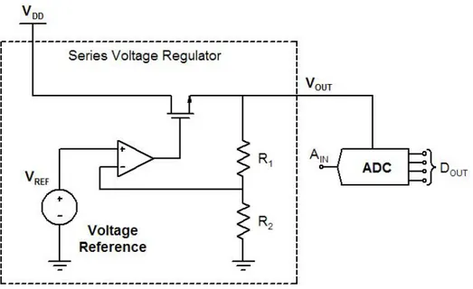
Voltage reference circuits are widely used in Analog to Digital Converters (ADCs) [58], see Fig. 3.1. A voltage regulator locks the output voltage (VOUT) to the
reference voltage generated by means of a resistor ratio,
2 1 2 OUT REF
R
R
V
V
R
. (3.1)Actually it is a two-stage feedback amplifier with a reference voltage as an input. The first stage is an op-amp and the second stage is a source follower. Depending on its aspect ratio, this source follower can deliver a large current to the ADC. The supply voltage, VDD, usually contains a ripple that is suppressed by the regulator.
The accuracy of the output voltage, sent to the ADC, depends on both accuracies of the resistor ratio and the reference voltage (VREF). The resistor ratio can have a
smaller error than 0.1% [59]. As a result, the final accuracy will depend on the absolute error of VREF.
The most common solution for on-chip integration is the Bandgap Voltage Reference (BGR), which can be implemented in standard CMOS technology exploiting parasitic vertical BJTs. Conventional BGRs generate a nearly temperature independent reference, of about 1.25 V, and therefore they require a higher supply voltage, which might not meet the low-voltage constraints for low-power applications. However, several solutions, exploiting the BGR principle, have been implemented that ensure sub-1V operation [47]. In [24, 48, 49] the reference voltage is lowered by means of resistive subdivision. As an alternative approach, floating gate structures have been used to realize high precision programmable voltage references, as in the case of [50], where subthreshold operation allowed a minimum power consumption of 1.35 µW. Most often forward biased PN-junctions of BGRs are substituted with MOSFETs biased in the
29
subthreshold region [51-53]. Thus, a supply voltage (VDD) of 0.6 V and a power
consumption of 9 µW are achieved. Other solutions have been implemented in standard CMOS technology, without exploiting the traditional BGR principle [18, 54-57]. Subthreshold operation allowed sub-1µW power consumption [18, 55-57] and sub-1V operation [18,57].
In this section the typical parameters of performance and figures of merit of voltage reference architectures are described. The operating principles of BGR and sub-1-V configurations are shown. Subsequently it is presented how subthreshold operation has been successfully exploited in low voltage, low power voltage reference circuits. At first, circuit solutions exploiting the BGR principle by means of subthreshold operated MOSFETs, instead of bipolar transistor, are presented. Then ultra low power, low voltage architectures working in weak inversion regime, without exploiting the BGR principle, are shown. Afterwards the proposed CMOS voltage reference configurations operating with all transistors biased in subthreshold region are introduced. Their novel operating principle and circuit architectures are described in detail. Then design considerations are discussed and, finally, experimental results are shown and compared with low voltage, low power competitors found in the scientific literature.
3.2. Performance specifications
A voltage reference is an analog block that provides a stable DC voltage, VREF,
starting from a less stable supply voltage VDD. Apart from general key performance
indicators of integrated circuits such as power consumption and Si area occupation, voltage reference circuits typically have stringent accuracy requirements. Usually, deviations from the expected value of the generated reference voltage are mainly due to temperature and supply voltage variations, process variations, spurious signal from power lines and noise generated by active devices within the voltage reference circuit.
30
3.2.1. Line sensitivity
The line sensitivity (LS) is the capability of the circuit to maintain a stable output
despite VDD variations. A ΔVREF change resulting from a variation of the supply
voltage of ΔVDD gives a line sensitivity of, REF DD
V
LS
V
. (3.2)It is usually expressed as mV/V or µV/V. An alternative definition is based on the percentage change of VREF,
%
100
REF REF DDV
V
LS
V
, (3.3) expressed as %/V. 3.2.2. Temperature coefficientThe temperature coefficient (TC) gives a measure of the ability of the voltage
reference to maintain the expected VREF under varying thermal conditions. Similarly
to LS, it is defined in two forms,
[mV/°C or V/°C]
REFV
TC
T
, (3.4)
%
10
6V
REFV
REF[ppm/°C]
TC
T
. (3.5)Where ΔT express the change in temperature which has the consequent ΔVREF
change.
3.2.3. Power Supply Rejection Ratio
The Power Supply Rejection Ratio expresses the capability of the circuit to reject noise coming from power supply. It is evaluated as the small signal ratio between the output voltage and the power supply,
20log
ref[dB]
ddv
PSRR
v
, (3.6) 3.2.4. Other specificationsOther performance indicators are the equivalent output noise generated by the circuit over frequency, the process variation effects that cause a dispersion of the
VREF value and the long term stability drift. Namely the latter measures the VREF
variation over a long period of time at some specified condition of steady state operation.
3.3. Bandgap References (BGRs)
Bandgap reference voltage circuits are one of the most widely used analog circuits in memories, ADCs and power management circuits. They exhibit very little dependence on temperature and, since most process parameters vary with