Universit`
a degli Studi di Salerno
FACOLT `A DI SCIENZE MATEMATICHE, FISICHE E NATURALI Dipartimento di Fisica “E.R. Caianiello”
Tesi di Dottorato di Ricerca in Fisica
X ciclo - Nuova Serie (2008-2011)Nb nanoporous ultrathin films:
matching effects and interconnected wires
Michela Trezza
Advisor:
Prof. Carmine Attanasio
Universit`a degli Studi di SalernoCoordinatore:
Prof. Giuseppe Grella
Universit`a degli Studi di SalernoContents
Introduction 1
Bibliography 5
1 Theoretical and experimental background 9
1.1 Brief review of superconductivity . . . 10
1.2 Key properties of vortices . . . 15
1.3 Superconducting nanostructures for controlling vortex dynamics . . . . 17
1.3.1 Pinning due to antidots . . . 18
1.3.2 Magnetic dots . . . 27
1.4 Superconductivity in one dimension . . . 37
1.4.1 Phase slips in one dimension . . . 38
1.4.2 Free energy barrier . . . 40
1.4.3 Appearance of resistance in 1D superconducting wire . . . 44
1.4.4 Quantum phase slips . . . 52
1.4.5 Other properties of 1D superconducting nanowire . . . 59
Bibliography 67 2 Fundamentals of porous silicon and applications 75 2.1 History of porous silicon . . . 75
2.2 Basics of the porous silicon formation process . . . 77
2.2.1 Electrochemical etching of porous silicon . . . 77
2.2.2 Chemistry of the formation of porous silicon . . . 80
Bibliography 89
3 Matching effects: experimental results 93
3.1 Evidence of fractional matching states . . . 94
3.1.1 Sample fabrication . . . 96
3.1.2 Experimental results and discussion . . . 97
3.2 Jc enhancement due to antidots . . . 109
3.2.1 Sample fabrication . . . 110
3.2.2 Experimental results and discussion . . . 112
Bibliography 117 4 Vortex pinning with artificial magnetic nanostructures 121 4.1 Introduction . . . 121
4.2 Sample fabrication . . . 123
4.3 Experimental results and discussion . . . 127
Bibliography 133 5 1D superconductivity in porous Nb ultrathin films 135 5.1 Introduction . . . 135
5.2 Sample fabrication . . . 137
5.3 Experimental results and discussion . . . 138
5.3.1 Resistive transition . . . 139 5.3.2 I-V measurements . . . . 142 Bibliography 145 Conclusions 149 Publications 151 ii
Acknowledgments 153
Introduction
When the applied magnetic field is higher than the lower critical field but below the upper critical field, a type-II superconductor allows magnetic flux to penetrate it in the form of vortices, a tiny normal area surrounded by supercurrents. Driven by the Lorentz force of a passing external current or by thermal activation, vortices can move. Their motion induces energy dissipation and eventually can destroy the super-conductivity. Recent advances in nanofabrication have led to tremendous possibilities for implementing superconducting pinning structures and controlling the motion of vortices. The dynamics of vortices in confined superconducting geometries has gener-ated much interest, including studies of fundamental properties about vortex matter and devices based on the motion of the vortices. During the past decades, a lot of efforts have been devoted to introducing artificial pinning centers into superconductors to stabilize and pin the vortex lattice against the external driving force, thus giving rise to higher critical currents [1–10]. This is of practical importance since super-conductors are required to maintain high critical currents for potential technological applications. Generally there are two different kinds of artificial pinning centers. The first one are the random imperfections, for example heavy-ion radiation damage [11], cold work induced dislocations [12], disordered hole arrays [13–15], etc. The other one are periodic defect arrays such as antidots (holes) [1–4, 7, 16], dots [6], and magnetic dots [5, 17, 18].
Recent advances in micro- and nanofabrication technologies have made possible to produce superconductors with carefully controlled arrays of artificial defects [4–10, 19– 21] with pores size and interpore spacing comparable to the relevant length scales of
superconductors such as the coherence length ξ(T ) and the penetration depth λ(T ), which are generally under submicron scales. As one of the most efficient and easiest methods, introducing periodic hole arrays into superconducting films has attracted much interest [4, 7–9]. Moreover, superconducting films containing periodic hole ar-rays also provide a unique platform to understand vortex motion and pinning in the presence of regular pinning centers. The interplay between the periodic pinning forces and the elastic repulsive vortex-vortex interaction generates a variety of novel vortex phenomena such as the commensurate effect [19, 22], the rectification and phase lock-ing of the vortices [20], composite fluxline lattices [23], which are not observed in the continuous superconducting films.
The commensurate effect between the vortex lattice and the underlying periodic artificial pinning array is one of the intriguing properties in superconducting films with periodic hole arrays [7, 8, 23, 24]. It appears as minima in the magnetic field depen-dence of the resistance, R(H), or as maxima in the field dependepen-dence of the critical current, Ic(H), when the vortex lattice is commensurate with the underlying periodic
artificial pinning array, i.e., when the external magnetic field corresponds to integer multiples or fractions of the so-called first matching field H1. This effect is normally
interpreted as a result of the pinning enhancement [25–28], i.e., vortices are more diffi-cult to move at matching fields. Thus, a pinning enhancement occurs and high critical current (or resistance minima) are achieved. A similar effect has also been observed in superconducting wire networks [29–31]. The wire networks are one dimensional (1D) multiconnected superconducting thin strips whose width w is comparable to the superconducting coherence length ξ(T ). So, a superconducting film containing a peri-odic hole array can resemble a superconducting wire network at temperatures close to
Tc. Both these mechanisms have been used to interpret the commensurability effects
observed in transport measurements on superconducting films containing an array of holes at temperatures close to Tc. For example, in aluminum films containing periodic
hole arrays, Fiory et al. associated the magnetoresistance oscillations to commensu-rate vortex pinning [1], whereas Pannetier et al. attributed these oscillations to wire
3
network properties [30]. In order to understand the related physics and for possible applications, it is necessary to distinguish these two mechanisms and identify the real origin of the commensurability effect.
This thesis presents some investigation of vortex dynamics in superconducting Nb ultrathin films with different artificial pinning centers: magnetic and non-magnetic. Evidence of 1D superconductivity observed in these structures will be also discussed. In chapter 1, after a brief introduction to the main aspects of the superconductiv-ity, the relevant concepts of the vortex dynamics, such as flux-flow resistivity and the vortex pinning, are discussed. Implementation of artificial defects, including pinning holes, magnetic dots, and different pinning arrangements of periodic and quasi-periodic pinning arrays, are presented. Finally the basics of 1D superconductivity are intro-duced.
In chapter 2 the different stages of the porous silicon formation are explained. The anodization parameters that influence the final characteristics of the fabricated layers are also discussed and the porous silicon photoluminescence is briefly described.
In chapter 3 transport properties of perforated Nb ultrathin films deposited on porous silicon are presented. Resistive transitions and critical current measurements as a function of the applied magnetic field show matching effect between the vortex lattice and the structure of the pinning array.
In chapter 4 the electromagnetic interaction between the vortex lattice and mag-netic pinning centers in Nb films deposited on nanoporous Al2O3 substrates containing
an array of Ni nanowires was investigated by transport measurements in the presence of magnetic field applied perpendicularly to the samples surface. The (H,T ) phase diagram was studied for these systems and compared to the one of a plain Nb film.
In chapter 5, resistive transitions and current-voltage characteristics measured on perforated Nb ultrathin bridges deposited on porous Si are reported. Due to the reduced dimensions of the pores diameter as well as of the interpore distance the experimental observations strongly call to mind features of 1D superconductivity.
Bibliography
[1] A.T. Fiory, A.F. Hebard, and S. Somekh, Appl. Phys. Lett. 32, 73 (1978).
[2] A.N. Lykov, Solid State Commun. 86, 531 (1993).
[3] A. Castellanos, R. W¨ordenweber, G. Ockenfuss, A.v.d. Hart, and K. Keck, Appl. Phys. Lett. 71, 962 (1997).
[4] V.V. Moshchalkov, M. Baert, V.V. Metlushko, E. Rosseel, M.J. van Bael, K. Temst, Y. Bruynseraede, and R. Jonckheere, Phys. Rev. B 57, 3615 (1998).
[5] M.J. Van Bael, K. Temst, V.V. Moshchalkov, and Y. Bruynseraede, Phys. Rev. B 59, 14674 (1999).
[6] A. Hoffmann, P. Prieto, and I.K. Schuller, Phys. Rev. B 61, 6958 (2000).
[7] U. Welp, Z.L. Xiao, J.S. Jiang, V.K. Vlsko-Vlasov, S.D. Bader, and G.W. Crab-tree, Phys. Rev. B 66, 212507 (2002).
[8] T.C. Wu, P.C. Kang, L. Horng, J.C. Wu, and T.J. Yang, J. Appl. Phys. 95, 6696 (2004).
[9] S. Raedt, A.V. Silhanek, M.J. Van Bael, R. Jockheere, and V.V. Moshchalkov, Physica C 404, 298 (2004).
[10] J. Hua, Z.L. Xiao, D. Rosenmann, I. Beloborodov, U. Welp, W.K. Kwok, and G.W. Crabtree, Appl. Phys. Lett. 90, 072507 (2007).
[11] L. Civale, A.D. Marwick, T.K. Worthington, M.A. Kirk, J.R. Thompson, L. Krusin-Elbaum, Y. Sun, J.R. Clem, and F. Holtzberg, Phys. Rev. Lett. 67, 648 (1991).
[12] J.W. Ekin, J. Appl. Phys. 62, 4829 (1987).
[13] J. Hua, Z.L. Xiao, D. Rosenmann, I. Beloborodov, U. Welp, W.K. Kwok, and G.W. Crabtree, Appl. Phys. Lett. 90, 072507 (2007).
[14] M. Trezza, S.L. Prischepa, C. Cirillo, R. Fittipaldi, M. Sarno, D. Sannino, P. Ciambelli, M.B.S. Hesselberth, S.K. Lazarouk, A.V. Dolbik, V.E. Borisenko, and C. Attanasio, J. Appl. Phys. 104, 083917 (2008).
[15] M. Trezza, S.L. Prischepa, C. Cirillo, and C. Attanasio, Europhys. Lett. 88, 57006 (2009).
[16] J. Eisenmenger, M. Oettinger, C. Pfahler, A. Plettl, P. Walther, and P. Ziemann, Phys. Rev. B 75, 144514 (2007).
[17] J.I. Mart´ın, M. V´elez, J. Nogu´es and I.K. Schuller, Phys. Rev. Lett. 79, 1929 (1997).
[18] M. V´elez, J.I. Mart´ın, J.E. Villegas, A. Hoffmann, E.M. Gonz´ales, J.L. Vincent and I.K. Schuller, J. Magn. Magn. Mater. 320, 2547 (2008).
[19] U. Welp, Z.L. Xiao, V. Novosad, and V.K. Vlasko-Vlasov, Phys. Rev. B 71, 14505 (2005).
[20] J. Van de Vondel, C.C. de Souza Silva, B.Y. Zhu, M. Morelle, and V.V. Moshchalkov, Phys. Rev. Lett. 94, 57003 (2005).
[21] G.R. Berdiyorov, M.V. Milosevic, and F.M. Peeters, Phys. Rev. B 74, 174512 (2006).
7
[22] V.V. Metlushko, U. Welp, G.W. Crabtree, Zhao Zhang, S.R.J. Brueck, B. Watkins, L.E. DeLong, B. Ilic, K. Chung, and P.J. Hesketh, Phys. Rev. B 59, 603 (1999).
[23] M. Baert, V.V. Metlushko, R. Jonckheere, V.V. Moshchalkov, and Y. Bruynser-aede, Phys. Rev. Lett. 74, 3269 (1995).
[24] K. Harada, O. Kamimura, H. Kasai, T. Matsuda, A. Tonomua, and V.V.
Moshchalkov, Science 274, 1167 (1996).
[25] Z. Jiang, D.A. Dikin, V. Chandrasekhar, V.V. Metlushko, and V.V.
Moshchalkov, Appl. Phys. Lett. 84, 5371 (2004).
[26] W. Vinckx, J. Vanacken, V.V. Moshchalkov, S. Tempfli, M. M´at´efi-Tempfli, S. Michotte, and L. Piraux, Eur. Phys. J. B 53, 199 (2006).
[27] A. Terentiev, D.B. Watkins, L.E. De Long, L.D. Cooley, D.J. Morgan, and J.B. Ketterson, Phys. Rev. B 61, 9249 (2000).
[28] M. Velez, D. Jaque, J.I. Martin, F. Guinea, and J.L. Vicent, Phys. Rev. B 65, 94509 (2002).
[29] A. Bezryadin and B. Pannetier, J. Low Temp. Phys. 98, 251 (1995).
[30] A. Bezryadin and B. Pannetier, J. Low Temp. Phys. 102, 73 (1996).
[31] A.N. Grigorenko, G.D. Howells, S.J. Bending, J. Bekaert, M.J. Van Bael, L. Van Look, V.V. Moshchalkov, Y. Bruynseraede, G. Borghs, I.I. Kaya, and R.A. Stradling, Phys. Rev. B 63, 052504 (2001).
Chapter 1
Theoretical and experimental
background
In this chapter, firstly a brief review of the superconductivity is presented, includ-ing the Meissner effect, the phenomenological description of superconductivity, the Ginzburg-Landau theory and the BCS microscopic theory. I also discuss the vortex response in a superconductor and the relevant concepts for describing vortex dynam-ics, such as the flux-flow resistivity and the vortex pinning by defects. I continue with a review of some recent results connected to the pinning in superconductors. Both theoretical and experimental investigations will be included. I discuss different im-plementations of artificial pinning in superconducting films, including holes, magnetic dots, and different arrangements of periodic and quasi-periodic pinning arrays. Then I introduce the basics of superconductivity in one dimension (1D). A review of the studies on 1D superconducting wires will be presented. I discuss various theoretical proposals and the corresponding experimental implementations.
1.1
Brief review of superconductivity
One hundred years ago on April 8, 1911, H. Kamerlingh Onnes discovered super-conductivity in liquid helium in Leiden, where zero resistivity of mercury was measured (Fig. 1.1) [1]. In his notebook, he wrote resistance practically zero. He referred to the phenomenon of zero resistivity as superconductivity. Subsequent measurements of the resistance for other materials at the liquid helium temperature were performed, and many metals and alloys were found to be superconducting below a well-defined critical transition temperature Tc. A second fundamental hallmark associated with
a superconductor is the exclusion of magnetic flux, discovered by W. Meissner and R. Ochsenfeld in 1933. The combination of zero resistance and perfect diamagnetism results in a clear distinction between a superconductor and a hypothetical perfect conductor; this difference involves the different response that each would have for dif-ferent histories of cooling below the transition temperature and applying a magnetic field. If we start by cooling through Tc and then apply a magnetic field, both the
superconductor and the perfect conductor would exclude the field.
Figure 1.1: Resistive transition of mercury as measured by Kamerlingh Onnes.
1.1. Brief review of superconductivity 11
superconductor and the perfect conductor behave differently, the superconductor ex-cludes the flux whereas the perfect conductor would remain fully permeated by the field. These observations argue that the transition associated with superconductivity is a phase transition independent of its history.
However, perfect conductivity, and with it the Meissner effect, does not persist to arbitrarily high magnetic fields [2]. For each temperature there is a well-defined critical field Hc(T ), at which superconductivity disappears. Figure 1.2 shows an universal
curve of the temperature dependence of Hc. The temperature dependence of the
critical field Hc, for many superconductors, is well described by the empirical relation
Hc(T ) = Hc(0) " 1 − Ã T Tc !2# (1.1)
Figure 1.2: The temperature dependence of the critical field.
The first successful phenomenological theory of superconductivity was published in 1935 by brothers F. and H. London. Their theory described two basic electrodynamic properties of superconductivity concerning the characteristics of a perfect conductivity and the Meissner effect. The second London equation also introduced the penetration depth λ(0), characterizing a length scale over which a magnetic field exponentially decreases into the superconductor at zero temperature. The temperature dependence
of λ(T ) in terms of λ(0) can be written, as the temperature approaches Tc, as λ(T ) = λ(0) Ã 1 − T Tc !−1/2 (1.2)
In 1952, V.L. Ginzburg and L. Landau (GL) introduced a mathematical theory of the superconducting phase transition which does not purport to explain the microscopic mechanisms giving rise to superconductivity. Instead, it examines the macroscopic properties of a superconductor with the aid of general thermodynamic arguments. Ginzburg and Landau argued that the free energy of a superconductor near the super-conducting transition can be expressed in terms of a complex order parameter ψ which described how deep into the superconducting phase the system is. In the GL theory the electrons that contribute to superconductivity were proposed to form a superfluid. In this interpretation |ψ|2 indicates the fraction of electrons that has condensed into a
superfluid. The GL equations produce many interesting and valid results. The most important of these is its prediction of the existence of another characteristic length in a superconductor: the coherence length ξ which characterizes the distance over which the superconducting order parameter can vary. The coherence length ξ is found to diverge as the temperature approaches Tc according to the expression:
ξ(T ) = ξ(0) Ã 1 − T Tc !−1/2 (1.3)
The ratio κ = λ/ξ is known as the Ginzburg-Landau parameter. It has been shown that type-I superconductors are those with 0 < κ < 1/√2 and type-II superconductors ones with κ > 1/√2. For type-II superconductors the phase transition from the normal state is of the second order, whereas for type-I it is of the first order.
In 1957, based on the GL theory, Abrikosov proved the existence of a so-called mixed state in type-II superconductors. In this mixed phase, above the first transition
1.1. Brief review of superconductivity 13
field Hc1, an increase in the flux density is expected until the magnetic field reaches
another critical field Hc2, eventually destroying the superconductivity and entering
the normal state (Fig. 1.3). Hc1 is called the lower critical field and Hc2 is the upper
critical field.
Figure 1.3: Phase diagram for a type-II superconductor.
Abrikosov found that in type-II superconductors in a high magnetic field, the field penetrates in quantized tubes of flux which are most commonly arranged in a hexagonal array as a consequence of a negative normal-superconductor interfacial energy. In order to maximize the contribution of interface energy, flux penetrates the superconductor in many discrete flux quanta or fluxons, each fluxon containing a single flux quantum given by
Φ0 = h
2e = 2.07 × 10
−15T m2 (1.4)
The structure of a fluxon consists of a short-range (of order ξ) normal core, where the order parameter vanishes, surrounded by a long-range (of order λ) vortex of supercor-rent.
the concept of the Cooper pairs in 1957 and the microscopic theory of superconduc-tivity finally moved a revolutionary step [3]. At the superconducting state, electrons tend to bind in pairs, thereby they have a lower energy level than in the Fermi-sea ground state. BCS theory starts from the assumption that there is some attraction between electrons, which can overcome the Coulomb repulsion. An electron moving through a conductor will attract the nearby positive charges in the lattice. This de-formation of the lattice causes another electron, with opposite spin, to move into the region of higher positive charge density. The two electrons then become correlated due to the Pauli exclusion principle. The electrons in Cooper pairs interact by exchanging phonons. The BCS theory predicted that a minimum energy Eg = 2∆(T ) is required
to break the Cooper pairs. ∆(T ) is the energy gap between the ground state and the quasi-particle excitations of the system and it is of the order of kBTc, where kB is
the Boltzmann constant. BCS theory correctly predicts the Meissner effect and the variation of the penetration depth with temperature. It also describes the variation of the critical magnetic field with temperature and relates the value of the critical field at zero temperature to the value of the transition temperature and the density of states at the Fermi energy. Moreover, the BCS theory reproduces the isotope effect, which is the experimental observation that, for a given superconducting material, the critical temperature is inversely proportional to the isotopic mass of the constituent element. In 1959, Gorkov was able to show that the GL theory is a limiting form of the BCS theory when the temperature is close to Tc [4].
1.2. Key properties of vortices 15
1.2
Key properties of vortices
As described previously, each vortex in type-II superconductors is surrounded by a circulating screening current. The vortices in a bulk superconductor are subject to a repulsive force from neighboring vortices due to the interaction with the circulating currents. As the applied magnetic field is increased further beyond Hc1, the density of
fluxons increases, and vortex-vortex repulsion, when the vortex space is comparable to the penetration depth λ, leads to the formation of a triangular array in order to maintain the lowest energy of inter-vortex interaction. The triangular lattice constant
a0 can be described as:
a0 = Ã 2 √ 3 !1/2s Φ0 B (1.5)
where B is the applied magnetic field.
In the presence of a transport current density J the flux line lattice of a supercon-ductor in the mixed state experiences a bulk Lorentz force FL = J × B. The Lorentz
force will cause the vortex motion, leading to energy dissipation and a non zero resis-tance. So, the flux flow of vortices leads to a dissipation, which can be characterized by the vortex viscosity:
η = Φ0Hc2 ρn
(1.6)
where ρn is the normal-state resistivity of the material. However, fluxons are easily
pinned by regions of weaker superconductivity, such as microstructural defects. A vector sum of these elementary pinning forces (fp) opposes the Lorentz force.
In order to have a type-II superconductor suitable for technological applications, so that it can carry high currents in the presence of the flux line without or with
little dissipation, the flux lines have to be pinned. This can be achieved usually by artificial means, such as dislocations, heavy-ion radiation damage, grain boundaries, etc. More recently, with the development in nanofabrication, submicron pinning holes or magnetic dots have been implemented in superconducting thin films in order to increase pinning force. When a perpendicular magnetic field is applied, the field in-duces vortices to enter the sample and their movement causes the resistance increases significantly. However, at certain special applied fields, the period of the vortex lattice coincides with the one of the hole array, resulting in a very stable state with all vortices pinned by the holes. Both the density and mobility of free vortices drop dramatically to a level comparable to the zero field situation. The commensurate effect is one of the intriguing properties in superconducting films with periodic hole arrays [5–8]. It appears as minima in the magnetic field dependence of the resistance, R(H), or as maxima in the field dependence of the critical current, Ic(H), when the vortex lattice
is commensurate with the underlying periodic artificial pinning array, i.e., when the external magnetic field corresponds to integer multiples or fractions of the so-called first matching field H1, where H1 = Φ0/A is defined as one flux quantum, Φ0 = h/2e,
per unit cell area, A, of the pinning array. This effect is normally interpreted as a result of the pinning enhancement [9–11], i.e., vortices are most difficult to move at matching fields. Thus, a pinning enhancement occurs and high critical current (or resistance minima) can be achieved.
When a vortex is near the inhomogeneities in superconductors, the force between the vortex and the defect tends to pin the vortex in place. A calculation carried out by Mkrtchyan and Schmidt [12] shows that it is always energetically favorable for a vortex to be attracted by a cavity in the superconductors before the number of trapped vortices reaches a critical value, which largely depends on the superconductor and the cavity parameters. With vortices pinned in the pinning centers, the superconductors can now sustain a finite current without flux motion and dissipation. The current at which the threshold force is required to cause vortex motion is referred to as the
1.3. Superconducting nanostructures for controlling vortex dynamics 17
The experimental implementation of artificial pinning sites in superconducting films will be discussed in more detail in the next section.
1.3
Superconducting nanostructures for controlling
vortex dynamics
Reducing the dissipation in type-II superconductors caused by the motion of vor-tices is an important issue for scientists. In order to achieve the lower dissipation, increasing the vortex pinning would be the first intuitive way to do so. Therefore a larger pinning force fp and a larger critical current density Jc will be achieved in
the superconductors, which can be useful for practical applications. Recent advances in nanofabrication have enabled implementations of artificial periodic vortex pinning lattices in superconducting films. Such structures are typically produced with defect arrays such as nanoscale holes through the film [5, 7, 13–18], dots [19], and magnetic dots [20–24]. These structures result in a substantial magnetic field dependence of the critical current.
The critical current in periodic pinning structures typically exhibits commensu-rate behavior with maxima when the applied magnetic field H corresponds to one flux quantum, Φ0, per unit cell area, a20, of the pinning array, assuming that it is
square. Here a0 is the lattice constant of the pinning arrangement. For fields far from
these matching values, the dynamics of interstitial vortices, which are not located on the strong pinning sites but are more weakly confined through interactions with the strongly pinned vortices, lead to lower critical currents. Recently, a wide variety of experiments have been performed on such pinning arrays.
1.3.1
Pinning due to antidots
One approach for controlling the vortex motion in superconductors is to create submicron holes by using lithographic and etching techniques. These submicron holes are usually referred to as antidots in the thin films, which act as well-defined pinning centers. Mkrtchyan and Shmidt studied theoretically the interaction between a vortex and an antidot in a type-II superconductor [12]. Under the assumption that the hole radius is r ¿ λ, where λ is the penetration depth, capturing a single vortex by the pore is always energetically favorable. After a vortex has been captured, the vortex free energy undergoes a qualitative change, and it may result in a potential barrier between the vortex and the cavity so that the capture of subsequent vortices in the cavity largely depends on the superconductor and the cavity parameters, which could be energetically favored or not.
Therefore, the commensurate effect is often observed in superconductors containing periodic defect arrays. This effect represents itself as minima in the field dependence of the resistance, R(H) [25], or maxima in the field dependence of the critical current
Jc(H) [13, 15, 18, 26–28] at certain particular magnetic fields, Hn = nH1, where H1
is the first matching field, n is an integer which corresponds to the flux quantum number in each unit cell (Fig. 1.4). In some cases, the commensurate effect can also be observed even when n is a fractional number [29, 30]. An antidot with diameter Ø can trap at least one vortex [12, 31, 32], though the presence of the Bean-Livingstone barrier around the holes makes the entrance of a fluxon in some cases very difficult, especially at low temperature [29]. If the holes are sufficiently large, they can pin multiquanta vortices [32] up to a saturation number nS given by nS = Ø/4ξS(T ),
where ξS(T ) is the temperature dependent superconducting coherence length [12]; it
is defined as the maximum number of vortices that fits into a pore with diameter Ø. Therefore, the limiting number of the flux lines which can be pinned by a hole can be controlled by varying temperature (in this way ξS(T ) varies) or by changing the size
1.3. Superconducting nanostructures for controlling vortex dynamics 19
Figure 1.4: Critical current density and critical current (inset) as a function of magnetic field for YBCO films with and without antidots. The magnetic field is oriented normal to the film surface a T = 0.95 Tc. The matching fields are indicated by the solid and dashed
arrows for decreasing and increasing magnetic field, respectively [15].
Before discussing some experiments on the pinning structures, it is worth noting that all the experiments involving superconductors with antidots have to be performed very close to Tc to avoid that the background pinning in the film reduces the influence of
pinning from the antidots [33].
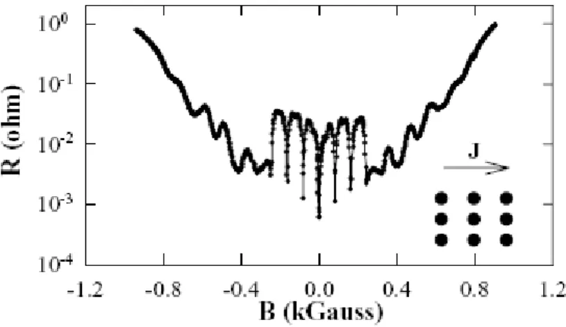
The composite flux-line lattices consisting of single or multiquanta vortices at the antidots and single vortices at interstitial positions have been studied by Baert et al. [7] in superconducting Pb/Ge multilayers with a square lattice of submicron holes. The authors demonstrated that the periodic arrays of antidots could be successfully used in order to stabilize such composite flux phases. They have investigated the vortices pinned at the holes and at the interstitial positions and then they have found that the mobility of the vortices at the interstices were strongly temperature dependent, which made it possible to see the transition between an insulating (fully localized vortices) and a metallic (a collective delocalized state) behavior by tuning the temperature.
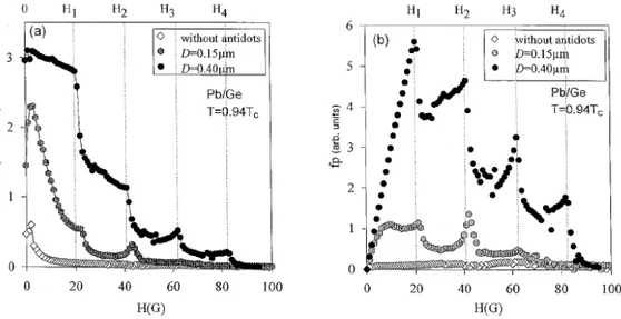
In order to find the optimum size for antidots, Moshchalkov et al. [16] introduced regular arrays of submicron holes in superconducting Pb/Ge multilayers and single
WGe films. Comparative measurements of critical current densities Jc and pinning
forces fp for several well-defined antidot diameters d have showed that pinning centers
with a size (diameter d) considerably larger than the temperature dependent supercon-ducting coherence length ξ(T ) are much more efficient than pinning centers with the diameter of the same order of ξ(T ) (Fig. 1.5). That is, antidots with a larger size than
ξ(T ) can provide a larger pinning force fp, and therefore provide a larger critical
cur-rent density Jc. Moreover, it was suggested from the experiments that the antidot size
realizing the optimum pinning was field dependent: smaller antidots optimize pinning in lower fields and larger antidots optimize pinning in higher fields. Crossover between different pinning regimes is controlled by the saturation number nS that defines the
largest possible number of flux lines trapped by an antidot.
Figure 1.5: The magnetization curves and pinning forces of the antidots with different diameters. The matching fields are indicated by dashed lines [16].
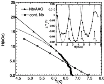
Welp et al. also have demonstrated that the perforated structure of anodized aluminum foils can provide a periodic pinning potential in superconductors [34]. In this work, Nb films containing triangular array of pores with 45 nm diameter and 100 nm interpore spacing have been fabricated using anodized aluminum oxide as substrate. Pronounced matching effects in the magnetization and periodic oscillations in the superconducting
1.3. Superconducting nanostructures for controlling vortex dynamics 21
critical temperature vs field were observed. Figure 1.6 shows the phase diagram of the porous Nb film and of a reference sample. One can immediately observe that the introduction of the dense hole array provided by the alumina template strongly modifies the superconducting phase of a plain Nb thin film [10, 34]. As a result, at the matching field, the upper critical magnetic field is increased at the matching values, as a consequence of the Little-Parks effect [35].
Figure 1.6: Superconducting phase diagram of the Nb/AAO sample (solid symbols) and of a continuous reference sample (open symbols). The inset shows the oscillatory variation of Tc(H) taken as the difference between the measured value and that obtained from the parabolic
fit. The first three matching fields are indicated [34].
A pronounced bump around H = H1 and weak shoulder at the second matching field H = H2 = 2H1 are observed. The non linear temperature variation of Hc2 of the
perforated film is well described by a parabolic dependence as shown by dashed line in Fig. 1.6. In order to improve the visualization of the periodic anomalies, the inset shows the R(T ) transition width as a function of the field. Cusps in ∆Tc occurring
periodically at multiples of the first matching field H1 are observed.
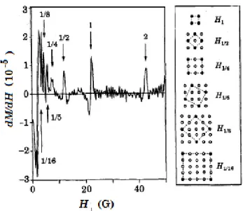
In some cases, the commensurability effects can also be observed even at fractional matching fields. Baert et al. [29] have studied flux phases in superconducting Pb/Ge
multilayers with a square lattice of submicrometer holes. Sharp peaks in the magnetic field dependence of the critical current at integer and fractional matching fields have been observed. At integer fields an artificial flux line crystal is formed, consisting of a stable square lattice of single or multiple flux quanta trapped by the antidots. Moreover, fractional flux lines patterns at H = Hk/l have been identified. Since the
holes act as very strong pinning centers, the distribution of the fluxons is determined by the available square pattern of holes. The optimization of the vortices positions for
H < H1 leads to the formation of larger square flux lattices with the period ak/l with
sites exactly falling onto the sites of the square lattice of pores with period a (Fig. 1.7).
Figure 1.7: On the left side, the derivative dM/dH for a Pb/Ge multilayer with a square lattice of holes is shown. The matching fields are indicated by the arrows. On the right side, the corresponding flux patterns, for the fractional quantization, for one unit cell are shown. The filled holes represent the holes occupied by vortices [29].
Both the pinning properties of square and rectangular arrays were simulated numer-ically by Reichhardt et al. [36]. In both cases, the critical depinning force shows maxima only at certain integer matching fields where the vortices can form highly ordered lattices. For rectangular arrays the depinning force and the commensurability
1.3. Superconducting nanostructures for controlling vortex dynamics 23
effects are anisotropic, with a higher depinning force along the long direction, where the matching effects were considerably reduced. The authors also found that for higher fields, the matching effects were reduced and certain peaks were absent.
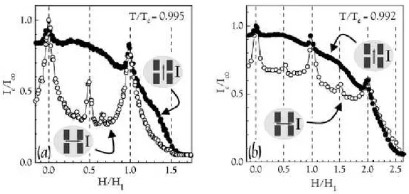
The anisotropy in the depinning force and the commensurability effects were experi-mentally realized by Van Look et al. [37]. Instead of employing rectangular pinning ar-rays, authors in this paper presented measurements on square arrays with rectangular shaped submicron holes, fabricated on a superconductor Pb film by an electron-beam lithography and etching. In this work two types of antidots are considered: antidots fully perforating the superconducting films and the ones that perforate the film only up to a certain depth. In both systems, they observed a distinct anisotropy in the pinning properties, reflected in the critical current Jc, which depend on the direction
of the applied electrical current. Although the mechanism responsible for the effect is very different in the two systems, they both show a higher critical current when the current is applied along the long side of the rectangular antidots. In the case of rectan-gular antidots fully perforating the superconductor, the vortex-vortex interaction was found to be anisotropic, which was responsible for the higher critical current. On the contrary, the vortex-vortex interaction was isotropic for the case of rectangular blind antidots. Instead, the shape of the pinning sites and the fact that a vortex could move around freely within the blind antidots is the cause of the anisotropy in the critical current (Fig. 1.8).
Figure 1.8: Normalized critical current Icx and Icy as a function of normalized magnetic field H/H1 measured with a current in the x (open symbols) and y directions (solid symbols),
respectively. Where (a) T /Tc = 0.995 and (b) T /Tc = 0.992, and H1 is the first matching
field [37].
The enhancement of the flux pinning strength at the pinning holes is widely assumed to be responsible for the critical current enhancement. However Patel et al. [38] claimed that the origin of the matching effect in such systems could be a hole-induced suppression of the critical temperature. Superconducting Nb films containing regular triangular arrays of antidots were investigated near the zero-field critical temperature. The authors found dips in the resistance vs magnetic field curves at matching fields where the magnitude of magnetic flux threading each unit cell is an integer number of the flux quantum. By comparing the magnetic field dependence of the resistance and critical temperature in perpendicular and parallel magnetic field directions, they observed that the matching effects in porous Nb films originated from hole-induced suppression of the critical temperature rather than the widely assumed flux pinning enhancement. The baseline derived is based on a wire network analysis matched to the R(H) curves (Fig. 1.9). In fact, a superconducting film containing a periodic hole array should resemble a superconducting wire network [19, 39, 40] when the width w of superconducting strips forming between the pores is comparable to the superconducting coherence length ξ.
1.3. Superconducting nanostructures for controlling vortex dynamics 25
Figure 1.9: Theory proposal and measurements in order to demonstrate the origin of anti-dots pinning enhancement. (a) A schematic approach to identify the origin of the resistance dips in R(H) curves at integer matching fields. The solid circles represent typical experimen-tal measurements. The dashed and solid curves are reference baselines expected for pinning enhancement at matching fields and hole-induced Tc suppression at non integer flux quantum
fields (wire network), respectively. (b) R(H) curves at T /Tc = 0.97 and H(T) phase diagram
(inset). Both curves R(H) and H(T) obtained in parallel fields (open circles) form the wire network baselines for those in perpendicular fields (solid circles) [38].
In addition to the studies of square and triangular arrays, Misko et al. [41, 42] have studied the critical current Jc as a function of the applied magnetic field Φ0 for quasi
periodic pinning arrays, such as one dimensional chains and two dimensional array of pinning centers placed on the nodes of a fivefold Penrose lattice (Fig. 1.10). The enhancement of the critical current was observed in the simulation results, suggesting that the Penrose lattice of pinning sites provides huge increase in Jc(Φ0) even compared
to triangular pinning arrays. Moreover, it is worth underlining that the Penrose lattice provides a tool to control the magnitude, sharpness and position of the peaks of Jc(Φ0).
Figure 1.10: The structure of a fivefold Penrose lattice. (a) The elemental building blocks are rhombuses with equal sides a and angles which are multiples of θ = 36◦. (b) There are rhombuses of two kinds: those having angles 2θ and 3θ (so called thick), and rhombuses with angles θ and 4θ (so called thin) [42].
Later, experiments for studying such fivefold Penrose pinning arrays were carried out [43–45]. A direct comparison of three different periodic arrays and quasi-periodic pin-ning arrays of antidots in superconducting Nb films has been investigated by Kemmler et al. [45]. In this experiment, the essential features in the Ic(H) patterns as predicted
by Misko et al. [41] were confirmed. A significant enhancement in Ic(H) was found
for quasi periodic pinning arrays in comparison to the one in samples with randomly distributed antidots or not antidots, but not as strong as triangular hole lattices (Fig. 1.11). In contrast to the plain and random samples the Penrose and triangular arrays showed clear matching effects, with identical first matching field H1. The triangular
array showed very pronounced matching peaks at H1 and H2. Instead, it is worth
underlining that for Penrose lattice it was possible to have a broader distribution in the magnetic field for the critical current enhancement. Comparing absolute values of
Ic for the Penrose and triangular array shows that very close to Tc critical currents at
H = 0, H1 and H2 are quite similar; however, due to the stronger reduction in Ic of
1.3. Superconducting nanostructures for controlling vortex dynamics 27
is superior, in particular, for small fields, below H1. The random sample always gives
significantly smaller Ic than the triangular and Penrose arrays.
Figure 1.11: Comparison of four different antidots arrangements of the magnetic field de-pendence of the critical current Ic. Insets: I vs V at H = 0 (right) and H = H1 (left)
[45].
1.3.2
Magnetic dots
A different approach rather than using antidots for introducing pinning centers in the superconductors is to utilize submicron magnetic dots [8, 46, 47]. The magnetic character of the dots can induce stronger pinning effects than similar non magnetic pinning centers [22]. In addition, large enough dot magnetization may create vortices in the superconducting film. This results not only in the observation of clear pin-ning effects when the vortex lattice interacts with the array of the magnetic dots but also it has been observed a rich behavior of the vortex dynamics that can be tuned by modifying the properties of the pinning array [22]. The ability to tune in situ the pinning potentials via changes of the magnetic configuration presents an unique opportunity provided by magnetic pinning centers. Martin et al. [48] first reported
the study of the pinning interaction between the vortex lattice and ordered arrays of submicron magnetic dots. In their work, triangular arrays of magnetic dots have been fabricated by electron beam lithography to study pinning effects on Nb thin films. The resistivity versus magnetic field shows a set of minima at constant field intervals. Every minimum appears when there is an integer number of vortices per unit cell of the array of magnetic dots (Fig. 1.12). The nature of the pinning mechanism induced by magnetic dots was principally determined either by a magnetic interaction between the magnetic dot and the magnetic moment of the vortex, or by a local suppression of the superconductivity due to the ferromagnetic proximity around the magnetic dot. The authors also pointed out that no indication of periodic pinning has been found in arrays of non magnetic dots measured at similar temperatures, current and field ranges, suggesting that the pinning due to the ordinary proximity effect is too weak to be observed. This confirms that the effects produced by the array of the Ni dots are mainly of magnetic origin. Moreover, they argue that the pinning is more relevant in the temperature range where the coherence length, ξ, is close to the size of the pinning site.
Figure 1.12: Field dependence of the resistivity of a Nb thin film with a triangular array of Ni dots. Inset shows the position of the minima versus the index number n [48].
1.3. Superconducting nanostructures for controlling vortex dynamics 29
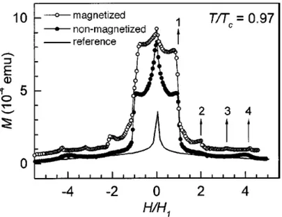
Similar magnetic dots were studied by Van Bael et al. [20] by utilizing magnetization hysteresis loop measurements. They report on the magnetic properties of elongated submicron magnetic islands and their influence on a superconducting film. Periodic lattices of Co islands act as efficient artificial pinning arrays for the flux lines in a superconducting Pb film deposited on top of the Co islands. The influence of the magnetic state of the dots on their pinning efficiency is investigated in these films, before and after the Co dots are magnetized (Fig. 1.13).
Figure 1.13: Upper half of the magnetization loop M vs H/H1 at T /Tc = 0.97 for a Pb film
on a triangular lattice of Co dots before (filled symbols) and after (open symbols) magnetizing the dots, and for a reference Pb film (line) [20].
The magnetization is shown as function of H/H1, where H1 represents the first
match-ing field for which the density of flux lines equals the density of dots. This implies that an one-to-one matching of the triangular vortex lattice onto the pinning array can be established at the first matching field H1. The presence of the lattice of Co dots
results in a very strong enhancement of the width of the magnetization loop compared to the reference Pb film without dots. Moreover, pronounced anomalies are observed for T close to Tc at certain multiples of H1. These matching effects indicate that the
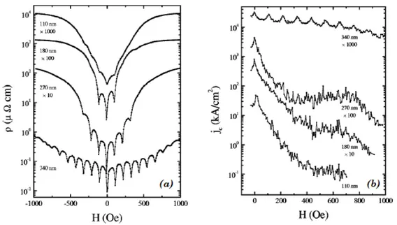
Pb film that is deposited on top of it, similar to thin films with an antidot lattice [20]. A systematic study about the influence of size and separation of the individual magnetic pinning centers has been developed by Hoffmann et al. [19]. While there is some dependence on the dot size, the periodic pinning changes its character drastically, as soon as the separation between dots becomes comparable to the coherence length of the superconductor. In addition, the comparison between the periodic pinning of magnetic dot arrays and non magnetic dot arrays shows that the former generally present more pronounced periodic pinning. This indicates conclusively a magnetic contribution to the pinning mechanism. Figure 1.14(a) shows the magnetoresistance
ρ(H) for four Nb films with the same thickness covering a same square array with
different Ni dot diameter. Magnetoresistance minima are observed for all samples at equidistant magnetic field intervals. For all four samples, the Ni dots were arranged on a square lattice with a lattice constant of 400 nm, thus the matching peaks occur for all samples at the same magnetic fields.
Figure 1.14: (a) The magnetoresistance ρ(H) for four Nb films with different Ni dot diameter and a square array with a lattice constant of 400 nm. (b) Magnetic field dependence of the critical current density Jc for Nb films with different Ni dot diameter and a square array
1.3. Superconducting nanostructures for controlling vortex dynamics 31
It is worth underlining that the periodic pinning becomes much more pronounced for larger magnetic dots. The number and depth of matching peaks increases with increas-ing dot diameter. This observation is generally independent from the temperature or bias current density [19]. Moreover, the magnetic field dependence of the critical cur-rent density Jc[see Fig. 1.14(b)] shows that the behavior of the sample with the largest
(340 nm) Ni dots is qualitatively different than the ones with smaller dots. Periodic critical current density matching peaks are only observed for the largest Ni dots, while the matching peaks are absent for the smaller ones. However, besides the increase in size there is also a decrease in the separation of the Ni dots, since for all the samples the lattice constant for the magnetic dot array is kept constant. Thus it is a priori not clear if the enhancement of the periodic pinning observed for the largest Ni dots is due to their size or their separation. Figure 1.15 shows the magnetoresistance for two samples with the same Nb thickness covering a same square array with a lattice constant of 600 nm and different Ni dot diameter.
Figure 1.15: Magnetoresistance curves for 100 nm thick Nb films with square arrays of Ni dots with dot diameter of 400 nm (top curve) and of 530 nm (bottom curve) [19].
Clearly, the sample with bigger dots shows many more matching peaks. In addition, more importantly for the sample with 400 nm Ni dots on a 600 nm square array (see
Fig. 1.15, upper curve) the matching effects are much less pronounced than for the sample with 340 nm Ni dots on a 400 nm square array [see Fig. 1.14(a), lowest curve]. This unambiguously shows that the dot separation and not the dot size is responsible for the strong enhancement of the periodic pinning effects [19].
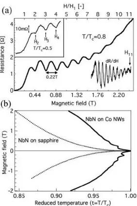
Another interesting work about matching effects linked to the magnetic antidots was presented by Hallet et al. [24]. Dense arrays of ordered ferromagnetic nanowires have been used to create periodic magnetic pinning centers in thin superconducting NbN films. Matching effects have been observed up to 2.5 T (11th matching field) and at low temperature. Also an appreciable enhancement of the superconducting properties has been recorded (Fig. 1.16).
Figure 1.16: (a) Magnetoresistance curve at T /Tc= 0.75 for a 25 nm thick NbN film on top
of an array of 75 nm in diameter Ni nanowires. Top inset: magnetoresistance curve at T /Tc
= 0.5. Bottom inset: derivative of the curve obtained at T /Tc = 0.75. (b) Phase diagram of a 25 nm thick NbN film deposited on top of an array of 60 nm in diameter Co nanowires (solid line) and on a flat sapphire substrate (dotted line) [24].
1.3. Superconducting nanostructures for controlling vortex dynamics 33
Numerous oscillations, caused by matching effects are visible, showing the strong in-fluence of the pinning center array on the vortex lattice. The oscillations are observed over the whole magnetic field range, i.e., up to 2.5 T as depicted from the derivative curve in the bottom inset. In addition, at the temperatures considered, the small spac-ing between the pinnspac-ing centers is of the order of the superconductspac-ing coherence length
ξ. As a result, the thin film behaves in fact more like an one dimensional wire network.
Such networks are known to show numerous matching effects since no vortices can be placed in the interstitial sites [24]. Figure 1.16(b) compares the superconducting phase diagram for a 25 nm thick NbN film sputtered on an array of Co nanowires (solid line) with the one obtained for the same NbN film deposited on a flat sapphire substrate (dotted line). Superconductivity takes place below the corresponding curves. The critical magnetic field is strongly enhanced, which means that the sample can be used at much higher fields before vortices start to move causing dissipation [24].
Instead of employing square magnetic pinning arrays, Martin et al. [49] have performed measurements on rectangular magnetic dot arrays obtaining very interesting effects. Magnetotransport reveals the existence of two pinning regimes that correspond to two types of resistivity minima with different constant field intervals (Fig. 1.17).
Figure 1.17: Field dependence of the resistivity of a Nb film with a rectangular array of Ni dots (a × b = 400 nm × 625 nm) measured at T /Tc = 0.98. A sketch of the current
The relation with the array lattice parameters indicates that a reconfiguration in the vortex lattice from rectangular to square is induced artificially by the interaction with the dot array. Two types of minima are clearly present; narrow and deep at low fields, whereas at higher fields (above 300 G) they are broader and shallower. Two different field regimes can be clearly identified. At low fields, the minima are sharp with spac-ing that corresponds well with the matchspac-ing field calculated for a rectangular vortex lattice with one vortex per unit cell. However, at high fields, the dissipation minima become broader and their spacing increases to a value which is close to the matching field of a square vortex lattice of parameter equal to the short side of the rectangu-lar array. Thus, at low fields, the vortex lattice is distorted by the strong pinning potential into a rectangular configuration that matches the Ni dot rectangular array
a × b cell, whereas at high fields vortex-vortex interactions become dominant and there
is a reconfiguration transition in the vortex lattice, which adopts a more symmetric square configuration that is only matched along the short side of the rectangular array cell [22]. A similar reconfiguration transition from low-field rectangular vortex lattice to high-field square has been observed in Nb films grown on a Si substrate with a rectangular array of non magnetic artificial defects [50]. However, in this case, the re-configuration field was significantly smaller than in a sample with a rectangular array of Ni dots of similar geometrical dimensions. This indicates again a reinforced pinning in the case of the magnetic dots in comparison with non magnetic defects.
Besides the reconfiguration transition, the anisotropy in the periodic pinning as a function of the direction of motion of the vortex lattice relative to the array may play an important role. Figure 1.18 shows the magnetoresistance of a Nb film on top of a 400 nm × 500 nm rectangular array of Ni dots with the transport current along the long and short sides of the rectangular array cell (i.e. θ = 0◦, solid symbols and
θ = 90◦, open symbols) [22]. The same matching field is found in both directions
caused by the commensuration condition of one vortex per unit cell. However, a clear anisotropy appears in the background dissipation at low fields (i.e. away from the matching conditions): the resistivity is much lower for θ = 90◦, i.e. when the vortex
1.3. Superconducting nanostructures for controlling vortex dynamics 35
lattice moves along the long side of the array cell, than for θ = 0◦, i.e. when the vortex
lattice moves along the short side of the array cell.
Figure 1.18: Magnetoresistance curves for a 100 nm thick Nb film with a (400 nm × 500 nm) rectangular array of Ni dots measured at T /Tc = 0.995 with the transport current along
the long and short sides of the rectangular array cell (i.e. θ = 0◦, solid symbols and θ = 90◦,
open symbols) [22].
This behavior has been predicted [36] by numerical simulations that indicate that a rectangular array of pinning centers induces an easy direction of motion for the vortex lattice along the short side of the array cell.
As I have already discussed before, the interaction between the vortex lattice and periodic arrays of pinning centers is stronger for particular, well-defined vortex den-sities, for which commensurability develops between the vortex lattice and the array. These matching effects appear as very sharp peaks (minima in the resistance or max-ima in the critical current) as a function of the applied magnetic field. This suggests collective vortex pinning and implies a high degree of order with long vortex lattice correlation lengths. However, commensurability effects between the vortex lattice with arrays lacking periodic order (quasi periodic and random arrays) have been recently observed, implying in some cases that local order is sufficient to induce matching
ef-fects. Villegas et al. [43] have investigated vortex lattice dynamics in superconducting Nb thin films with quasi periodic arrays of magnetic pinning centers. The magne-toresistance exhibits minima for well-defined applied fields, related to matching effects between the vortex lattice and the array [Fig. 1.19(b)].
Figure 1.19: (a) Scanning electron microscopy image of a pentagonal quasi periodic array of Ni dots. The inset shows a higher magnification image where self-similar pentagons are highlighted (blue and red).(b) Magnetoresistance of a 100 nm thick Nb film on top of a pentagonal quasi periodic array of Ni dots, at T /Tc = 0.985. Vertical lines mark the main minima. Inset: the curve as in (b) zoomed out [43].
The quasi periodic series of minima implies that the lattice adopts the pentagonal symmetry of the array at different length scales. The long period magnetoresistance oscillations imply matching to the array geometry over the length scale of the interdot distance [smaller (blue) pentagons in Fig. 1.19(a)], while the shorter period corre-sponds to commensurability over longer length scales [larger (red) pentagons in Fig. 1.19(a)].
1.4. Superconductivity in one dimension 37
1.4
Superconductivity in one dimension
Even if the subject of one dimensional (1D) superconductivity is many decades old, it continues to be a topic of great interest and a fundamental field in the condensed matter research area. The central challenge in the study of thin superconducting wires is to understand how the superconductivity is affected when approaching 1D limit. Continual advances in fabrication techniques have allowed researchers to create wires of ever shrinking size, resulting in an increasing number of observed effects that shed light on this basic question. Earlier studies have predicted that when the wire width is smaller than its phase coherence length ξ(T ) intrinsic thermal [51, 52] and quantum [53–55] fluctuations play an increasingly important role in this limit, causing the wires to remain resistive much below the superconducting transition temperature Tc. Phase
slip processes are responsible for resistance in superconducting nanowires. At high temperatures (but below the transition temperature Tc) this resistance is caused by
thermally activated phase slips (TAPS), namely the system makes a transition across a potential barrier between two different metastable states. At sufficiently low tem-peratures the general expectation is that the system would tunnel through the barrier between two metastable states, constituting a quantum phase slip event (QPS). Until now there are several experimental observations of TAPS which are in agreement with the predictions of the theoretical models. But observations of QPS remain a subject of strong debate. In the following I will first discuss the physics of phase slip phenomenon and then the models of TAPS and their experimental observation. The chapter ends with a discussion of theoretical models for QPS and by outlining some experimental works that claim observation of QPS.
1.4.1
Phase slips in one dimension
Within the phenomenological model of superconductivity proposed by Ginzburg and Landau (GL) in 1950, the superconducting electrons are described by the complex order parameter
ψ = ψ0eiφ (1.7)
where ψ0 is the magnitude and φ is the phase of the order parameter. The density of
the superconducting electrons is given by nS = |ψ|2 = ψ02, which is non zero below the
superconducting transition temperature Tc.
For a superconducting nanowire, in the absence of magnetic field, the supercurrent is driven by phase gradients, with a velocity given by
vS =
¯h
2m∇φ (1.8)
where m is the mass of the electrons. The supercurrent through a wire of cross sectional area A can be written as
IS = JSA = nSevSA = e¯h
2mψ
2
0∇φA (1.9)
Due to conservation of current we also have that ψ2
0∇φ = constant.
The process of phase slip was first introduced by Little in 1967 [56]. This theory was developed in order to understand the mechanism of the supercurrent decay in thin wires. Little’s argument is based on the assumption that the superconducting order parameter is defined locally as well as globally in a thin wire. The local amplitude of order parameter is subject to thermal fluctuations. As the order parameter reaches zero
1.4. Superconductivity in one dimension 39
somewhere along the 1D wire the phase changes by 2π in a process known as a phase slip. In figure 1.20 the complex order parameter ψ = |ψ(x)|eiφ(x) of a thin wire ring
is plotted as a function of the position x along the ring. Two possible configurations,
ψ0 (with no vortex, n = 0) and ψ1 (with one vortex, n = 1), are shown. ψ1 makes an
excursion around zero in the Argand plane near the point A while ψ0 does not make
such an excursion. The state ψ1 corresponds to a phase difference of 2π along the ring
and leads a nonzero supercurrent.
Figure 1.20: The superconducting order parameter is plotted as a function of the position along a superconducting ring. The two possible configurations shown correspond to the order parameter ψ0(x), with no vortex present in the ring (n = 0), and to the order parameter
ψ1(x), with one vortex present in the ring (n = 1). Near the point A, ψ1(x) makes an
excursion around zero on the Argand plane, while ψ0(x) does not. The transition from n =
1 to n = 0 constitutes a phase slip event. This event can be considered a vortex, with its normal core, passing across the wire. The transition between the n = 1 and n = 0 state can only occur if the order parameter reaches zero somewhere along the wire [56].
The state ψ0, on the other hand, corresponds to zero phase difference and corresponds
to zero net supercurrent. The transition from ψ1 to ψ0 constitutes a phase slip event
that topologically requires the order parameter curve to cross the x -axis. Precisely the condition ψ = 0 needs to be satisfied at some point in time along the wire. Hence, a phase slip event is equivalent to vortex core passing across the nanowire [57]. After each phase slip event, the phase difference between the ends of the wire can only change
by an integer multiple of 2π. The phase difference between the leads is defined by the number of times the order parameter goes around zero on the Argand plane. Little’s idea about phase slippage was further developed also in other works [51, 58, 59].
Within Little’s model, a finite resistance occurs at constant voltage bias, according to the following explanation. The voltage applied to the ends of the wires increases the phase difference between the wire, and thus tends to increase the supercurrent (Eq. 1.9). Simultaneously, the phase slips occurring stochastically at any point along the wire tend to decrease the supercurrent. A dynamic non-equilibrium steady state is reached at a supercurrent value that is linearly dependent on the applied voltage. This leads to a finite resistance. By the processes of phase slips the energy introduced by the voltage source is dissipated as heat rather than converted into kinetic energy of the supercurrent.
Thus, as I will discuss later, the process of phase slip leads to dissipation and the wire acquires a non-zero electrical resistance. This resistance is defined by an equation containing the temperature dependent energy barrier. This barrier is determined by the condensation energy required to locally suppress the order parameter to zero. The minimum energy barrier corresponds to fluctuations in which the order parameter is suppressed in wire segments with lengths of the order of coherence length ξ(T ). Hence TAPS causes nanowires to remain resistive at any nonzero temperature. In the following section the expression for the energy barrier for phase slip processes in a nanowire will be derived.
1.4.2
Free energy barrier
The calculation of the energy barrier for phase slips was done by Langer and Ambegaokar (LA) [58]. Using the time dependent GL theory, they found that the value of minimum free energy barrier that separates two stationary states of a 1D superconductor is
1.4. Superconductivity in one dimension 41 ∆F (T ) = 8 √ 2 3 H2 c(T ) 8π Aξ(T ) (1.10)
where Hc is the thermodynamical critical field, A is the cross sectional area of the
wire and ξ is the GL coherence length. The minimum volume over which the phase slip can occur is ∼ Aξ(T ) and the condensation energy involved is ∼ Aξ(T )H2
c(T )/8π.
Here, we have assumed that the diameter of the wire is smaller than the coherence length ξ such that entire cross section of the wire is normal during a phase slip process. Recalling that near Tc
Hc(T ) ∝ Ã 1 − T Tc ! (1.11) and ξ(T ) ∝ Ã 1 − T Tc !−1/2 (1.12)
Eq. 1.10 leads to temperature dependence of the barrier as
∆F (T ) = ∆F (0) Ã 1 − T Tc !3/2 (1.13)
Now we would like to find an expression for energy barrier comparable with the ex-perimental data; to do this we begin with ∆F (0) as
∆F (0) = 8 √ 2 3 H2 c(0) 8π Aξ(0) (1.14)
ξ2(T ) = ¯h2 4m|α(T )| (1.15) where α(T ) = −2e 2 mc2 H 2 c(T )λ2ef f(T ) (1.16)
with λef f the effective penetration depth and c the speed of light. At zero temperature
we have ξ2(0) = ¯h 2c2 8e2H2 c(0)λ2ef f(0) (1.17)
Thus, using this expression to eliminate Hc(0) from Eq. 1.14, we get
∆F (0) = 8 √ 2 3 1 8π ¯h2c2 8e2ξ2(0)λ2 ef f(0) Aξ(0) (1.18)
Recalling that, in the dirty limit
1 λ2 ef f(0) = l λ2 L(0)ξ0 (1.19)
where ξ0 is the Pippard coherence length, λL the London penetration depth and l the
mean free path, ∆F (0) becomes
∆F (0) = √ 2 3 A 8π ¯h2c2 e2ξ(0)λ2 L(0) l ξ0 (1.20)
1.4. Superconductivity in one dimension 43
At this point, we will eliminate the London penetration depth, given by
1 λ2 L(0) = 4πnS(0)e2 mc2 = 4πne2 mc2 (1.21)
where n is the density of the normal electrons. At zero temperature, almost all the electrons are paired and the density of superconducting electrons is equal to the total density of electrons nS(0) = n. The free energy barrier now becomes
∆F (0) = √ 2 3 A 2 ¯h2 e2ξ(0) l ξ0 ne2 m (1.22)
From the microscopic BCS theory
ξ0 = ¯hvF
π∆(0) (1.23)
where vF is the Fermi velocity and ∆(0) is the superconducting gap at zero
tempera-ture, so ∆F (0) = √ 2 3 π¯h 2e2 A ξ(0) ne2l mvF ∆(0) (1.24)
From Drude model of metals follows that the resistivity of a wire can be written as
1
ρ = ne2l mvF
(1.25)
and using this expression in Eq. 1.24 we arrive at
∆F (0) = √ 2 3 π¯h 2e2 A ξ(0) 1 ρ ∆(0) (1.26)
The BCS gap at zero temperature is given by ∆(0) ∼= 1.76kBTc. Thus, we get
∆F (0) = 0.83 RQ
RN
L
ξ(0) kBTc (1.27)
where RQ = π¯h/2e2 = h/4e2 is the quantum resistance of Cooper pairs and RN =
ρL/A is the normal state resistance of the wire with length L. As a final simplification,
we define a parameter c which allows us to express the free energy barrier as a function of temperature given as ∆F (T ) = ∆F (0) à 1 − T Tc !3/2 = c kBTc à 1 − T Tc !3/2 (1.28) where c = 0.83 RQ RN L ξ(0) (1.29)
1.4.3
Appearance of resistance in 1D superconducting wire
Superconducting nanowires never show zero resistance, although resistance does decrease exponentially upon cooling [51, 56, 58, 60–62] (see Fig. 1.21). The origin of this resistive behavior lies in the occurrence of thermally activated slips of the phase of the GL order parameter. During a phase slip, a small normal segment appears on the nanowire for a short time causing the loss of phase coherence [63]. Typical dimensions of such fluctuations are of the order of the superconducting coherence length. Generally, since the wire diameter is assumed smaller than the coherence length, it is clear that each such fluctuation should disrupt the flow of supercurrent and thereby impart a non zero resistance to the wire [64]. Such fluctuations are more commonly called thermally activated phase slips (TAPS) because the fluctuations
1.4. Superconductivity in one dimension 45
thermally activate the system over the free energy barrier, which changes the phase by 2π, thus providing the phase slip.
Figure 1.21: Resistance vs temperature curve of a nanowire of amorphous indium oxide, to-gether data obtained from a similarly prepared wide film. The transition is broad significantly more than one in similar 2D film, signaling the approach to the 1D limit. Inset: A scanning electron micrograph of a typical device [62].
In order to derive the resistance from TAPS we must first include the effect of the bias current in the wire. This makes the free energy landscape tilted, compared to the zero bias case (see Fig. 1.22).
Due to thermal fluctuations, the phase jumps over the barrier constituting a phase slip event. Because of the tilt the phase slip in one direction is more favorable than in the other as the energy barrier is lowered in one direction and increased in the other. The amount by which the free energy is lowered or raised was given by Anderson and Dayem [65] and it can be written as
δF = hI
![Figure 1.15: Magnetoresistance curves for 100 nm thick Nb films with square arrays of Ni dots with dot diameter of 400 nm (top curve) and of 530 nm (bottom curve) [19].](https://thumb-eu.123doks.com/thumbv2/123dokorg/7206100.76085/37.892.285.683.654.946/figure-magnetoresistance-curves-thick-square-arrays-diameter-curve.webp)
![Figure 1.23: Data (symbols) from Lukens, Warburton, and Webb [60] and their fit to LAMH theory (dashed line).](https://thumb-eu.123doks.com/thumbv2/123dokorg/7206100.76085/54.892.111.765.142.343/figure-data-symbols-lukens-warburton-webb-theory-dashed.webp)
