Autore:
Nico Costantino _______________
Relatori:
Prof. Luca Fanucci _____________
Prof. Sergio Saponara _____________
Ing. Guido Magazzù _____________
Design and Testing of Electronic Devices
for Harsh Environments
Anno 2013
UNIVERSITÀ DI PISA
Scuola di Dottorato in Ingegneria “Leonardo da Vinci”
Corso di Dottorato di Ricerca in
Ingegneria dell’Informazione
I
SOMMARIO
Questa tesi riporta una descrizione sintetica ed i principali risultati dell’attività condotta nell’ambito del programma triennale (2010-2012) di dottorato di ricerca in Ingegneria dell’Informazione presso l’Università di Pisa. L’attività di ricerca scientifica si è sviluppata in differenti settori, tra i quali Automotive ed esperimenti di Fisica delle Alte Energie, seguendo tuttavia un denominatore comune: lo sviluppo di dispositivi e sistemi elettronici per applicazioni sotto condizioni operative critiche.
Sono molteplici le applicazioni che forzano l’adozione di metodologie e strategie di design dedicate a questa tipologia di ambienti operativi: militari, biomediche, automobilistiche, industriali e spaziali. Lo studio di soluzioni mirate al soddisfacimento dei requisiti operativi specifici, rappresenta di conseguenza un interessante ambito di ricerca.
La prima attività di ricerca è stata inquadrata all’interno del progetto ATHENIS, finanziato dalla commissione CORDIS della Comunità Europea e finalizzato allo sviluppo di un System-on-Chip, un regolatore per alternatori per auto, in grado di unire ad un’innovativa flessibilità la capacità di lavorare sotto le condizioni operative più estreme adottate dall’industria automobilistica. In particolare è stato sviluppato un dispositivo denominato Intelligent Power Switch, in grado di pilotare carichi di diversa natura, quali lampadine ad incandescenza e LED, offrendo allo stesso tempo un alto livello di configurabilità ed adattabilità alle più estreme condizioni operative. Le numerose funzionalità che sono state integrate, tra cui la limitazione di corrente, la regolazione della tensione, la protezione dall’inversione di polarità e sovratensioni, l’accensione con slope controllato in corrente, unite a strategie di Over Current ed Over Temperature Protection, hanno richiesto la progettazione di un’architettura circuitale innovativa.
Il primo test-chip, realizzato in tecnologia AMS CMOS High Voltage 0.35 µm, è stato validato grazie allo sviluppo di un ambiente di test dedicato, che ha permesso la completa caratterizzazione del dispositivo evidenziandone le ottime prestazioni. Il secondo ramo di ricerca si è collocato all’interno del progetto FF-LYNX, che ha coinvolto la sezione di Pisa dell’Istituto Nazionale di Fisica Nucleare (INFN), il Dipartimento di Fisica dell’Università di California Santa Barbara (UCSB) ed il Centro Europeo per la Ricerca Nucleare (CERN). L’obiettivo di questo progetto multidisciplinare è stata la definizione di un protocollo per la distribuzione dei segnali di Timing, Trigger e Control e l’acquisizione dei dati di readout negli esperimenti di Fisica delle Alte Energie. Nello specifico, l’oggetto di studio è stato l’implementazione del protocollo in interfacce Transmitter-Receiver all’interno del test-chip FF-TC1, realizzato in tecnologia IBM CMOS 130 nm. Durante questa attività sono state studiate ed implementate tecniche di radiation hardening al fine di garantire il corretto funzionamento operativo in ambienti ad alto livello di radiazioni, come il Large Hadron Collider (LHC) presso il CERN di Ginevra. In aggiunta, è stato sviluppato un emulatore funzionale alla validazione del protocollo FF-LYNX, basato sulla board PLDA XpressGXII con interfacciamento PCI-Express ad un host-PC. Un’ulteriore attività ha riguardato l’adattamento dell’emulatore come test-bed per il test-chip FF-TC1, permettendone l’esecuzione di test funzionali estensivi. Sono stati infine effettuati test sotto irraggiamento presso la
X-II
rays facility del CERN, che hanno comprovato la bontà delle tecniche di radiation hardening implementate.
III
ABSTRACT
This thesis reports an overview and the main results of the research activity carried out within the PhD programme in Information Engineering of the University of Pisa (2010-2012). The research activity has been focused on different fields, including Automotive and High Energy Physics experiments, according to a common denominator: the development of electronic devices and systems operating in harsh environments.
There are many applications that force the adoption of design methodologies and strategies focused on this type of environments: military, biomedical, automotive, industrial and space. The development of solutions fulfilling specific operational requirements, therefore represents an interesting field of research.
The first research activity has been framed within the ATHENIS project, funded by the CORDIS Commission of the European Community, and aiming at the development of a System-on-Chip, a regulator for alternators employed on vehicles, presenting both configurability and the ability to work at the harshest operating conditions of the automotive industry. Specifically, a novel Intelligent Power Switch has been conceived, capable of driving different kind of loads, such as incandescent bulbs and LED, showing a high level of flexibility and adaptability to the most extreme operating conditions. Several features have been integrated, including current limitation, voltage regulation, reverse polarity and over-voltage capability, control of current slope, combined with strategies as over-current and over-temperature protection, that have required the design of an innovative architecture.
The first test-chip, realized in AMS CMOS High Voltage 0,35 µm technology, has been validated thanks to the development of a dedicated test-bed, which has allowed the deep characterization of the device, proving its excellent performance. The second branch of research has been carried out within the FF-LYNX project, which has involved the section of Pisa of the National Institute for Nuclear Physics (INFN), the Department of Physics of the University of California Santa Barbara (UCSB) and the European Organization for Nuclear Research (CERN). The aim of this multidisciplinary project has been the definition of a protocol for the distribution of Timing, Trigger and Control signals and for the readout in High Energy Physics experiments. In particular, the focus of the activity has been the implementation of the protocol into Transmitter-Receiver interfaces within the test-chip FF-TC1, realized in IBM CMOS 130 nm technology. During this phase, novel radiation hardening techniques have been studied and implemented in order to ensure the proper functioning in operating environments with a high level of radiation, such as the Large Hadron Collider (LHC) at CERN in Geneva. Besides that, an emulator for functional validation of the FF-LYNX protocol has been developed, embedded on the XpressGXII PLDA board, equipped with PCI-Express to interface with a host PC. An additional activity has required the modification of the emulator as a test-bed for the test-chip FF-TC1, allowing the execution of extensive functional tests. Finally, irradiation tests have been performed at the X-rays facility at CERN, which have demonstrated the good yield of the radiation hardening techniques implemented.
V
CONTENTS
INTRODUCTION ...1
1 ELECTRONIC DEVICES IN HARSH ENVIRONMENTS...3
1.1 Harsh Applications... ... 3
1.1.1 Automotive ... 3
1.1.2 Military ... 5
1.1.3 Space ... 6
1.2 Harsh Environments: Requirements And Constraints ... 8
1.2.1 Operating temperature ... 8
1.2.2 Particle radiation ... 10
2 HIGH ENERGY PHYSICS EXPERIMENTS: DEVELOPMENT, DESIGN AND TESTING FLOW OF AN INTEGRATED CIRCUIT...13
2.1 Introduction ...13
2.2 DAQ/TTC Systems for HEP experiments ... 15
2.3 Design Flow of Electronic Systems for HEP Applications ... 17
2.4 The FF-LYNX Protocol ... 20
2.5 FPGA-based Emulator ... 25
2.5.1 Emulator system ... 25
2.5.2 Functional emulation results ... 29
2.6 TX-RX Interfaces and Test Chip Design ... 31
2.6.1 FF-LYNX interfaces ... 31
2.6.2 Test chip architecture ... 35
2.6.3 Radiation hardening techniques ... 38
2.7 Test Chip Characterization ... 43
2.7.1 Test-bed structure ... 43
2.7.2 Total dose irradiation test setup and procedure ... 46
2.7.3 Functional characterization test ... 48
3 AUTOMOTIVE APPLICATION: DESIGN AND VALIDATION OF AN INTELLIGENT POWER SWITCH...50
VI
3.1 Intelligent Power Switches ... 50
3.2 Design flow of an IPS for Automotive Harshest Operating Conditions ... 54
3.2.1 Current limitation & over-current protection ... 56
3.2.2 Robustness against wiring parasitics effects ... 59
3.2.3 Limitation of EMI – Control of current slope ... 61
3.2.4 Harsh operating temperatures – Over-temperature protection ... 62
3.2.5 High voltage protection & reverse polarity capability... 62
3.3 IPS Implementation In Hv-Cmos And Test Set-Up ... 66
3.3.1 IPS implementation in HV-CMOS technology ... 66
3.3.2 Verification flow ... 66
3.4 Experimental Results ... 68
CONCLUSIONS ...73
1
INTRODUCTION
Harsh Environment applications represent an exciting new frontier, challenging the capabilities of designers of electronic devices. Extreme wide ranges of operating temperatures, high vibration levels, fluid exposure, moisture, high electromagnetic fields and hard transient disturbances represent some of the requirements and constraints for devices and systems employed in certain fields of application. The most critical ones are: military field, oil exploration systems, biomedical applications, automotive and space missions.
In order to fulfill such severe requirements, electronic designers for harsh environments need to follow design flows characterized by continuous steps of validation, at various levels, that will be described hereafter.
This thesis reports the main issues that have to be faced in the design of electronic devices and systems for harsh environments. The two research activities performed, have been focused on two of the harshest fields of applications: the automotive and the High Energy Physics (HEP) experiments. Besides the area, also the type of electronic devices developed are different: an analogue mixed-signal cell is the core of the first research activity in the automotive field, while a digital integrated circuit has constitued the result of the second branch, within the HEP field. In addition to the description of the hardening techniques and strategies implemented to make designed electronic devices suitable for the harsh environments, the overview of the two project flows represents a valuable content of this work.
Chapter 1 includes an overview of the harshest applications of electronic equipments, summarizing the main contraints of the automotive, military and space fields. A particular focus on operating temperatures and particle radiations is reported, since they represent the most critical issues to cope with in the conduction of the two research branches carried out during the PhD programme. The description of the development, design and testing flow of an integrated circuit to be employed in HEP experiments is the content of Chapter 2. An overview of the HEP experiments scenario is reported in Paragraphs 2.1, 2.2, 2.3. The main features of the novel FF-LYNX protocol have been reported in Paragraph 2.4, while Paragraph 2.5 shows the architecture of the FPGA-based emulator conceived to validate the main figures of merit of the protocol. Paragraph 2.6 presents the architecture of the TX and RX interfaces and of the test-chip FF-TC1, with details on the radiation hardening techniques applied during the design. Paragraph 2.7 is related to the test-chip characterization, describing the test-bed as well as some of the results of the functional test. The procedure used for the Total Ionizing Dose (TID) irradiation test and the behavior of the test-chip under X-ray irradiation are described in this paragraph as well.
The second case study is highlighted in Chapter 3, where a flexible device named Intelligent Power Switch (IPS) for automotive applications is described.
Paragraph 3.1 discusses the main advantages offered by this class of smart power modules and the relevant requirements to be faced when designing an IPS for automotive applications. Paragraph 3.2 presents the design-flow of the proposed IPS realized to safely handle ordinary or extraordinary electrical and environmental conditions. In Paragraph 3.3 the IPS implementation in HV-CMOS 0.35 µm process is shown as well as a description of the testing flow performed. Experimental measurements carried out on a test-chip in a lab and, exploiting a
2
mechatronic prototype, also in a real automotive environment, are described in Paragraph 3.4.
3
1
ELECTRONIC DEVICES IN HARSH ENVIRONMENTS
1.1
HARSH APPLICATIONS
Design of devices and systems for harsh environment applications represents a stimulating challenge for electronic engineers. In the current scenario, characterized by a constant demand for increasing processing capabilities, higher bandwidths and stricter reliability requirements, operating in a harsh environment forces the adoption of novel technologies and statregies. Several categories of harsh environments can be reported: military field including land-based, shipboard, airborne, missile-based applications; oil exploration systems; biomedical applications; automotive; space missions. Among these applications, the last one provides the best match in terms of the diversity of harsh environments and the need for low mass, and low power devices. The high variable space mission scenarios involve extreme exposures to mechanical shock and vibration loading, temperature, pressure, radiation, and chemical attack [1].
A brief description of the main fields of harsh application will be analyzed hereafter.
1.1.1 Automotive
Electronics for automotive works in one of the harshest environments, fulfilling extreme electrical constraints and ensuring high levels of reliability and durability, as the automotive manufacturers are offering extended warranties to consumers for 350,000 km/15 years or even more. Robustness against mechanical vibrations (up to 10Grms on engine), fluid exposure such as petroleum vapors and other chemicals, moisture, high electromagnetic fields and hard transient disturbances makes the automotive field extremely tough for electronic devices. Besides that, operating temperature at 125 °C under-hood and locally up to 175 °C, high voltage and reverse polarity capability, are critical additional requirements and constraints for systems and ICs designed to operate aboard a motor vehicle [28]–[33]. Obviously, the operating requirements to be fulfilled by an on-board IC depend on its position inside the vehicle. Maximum operating temperature shows a large spread based on the localization, starting from a value of 70 °C outside the cockpit, reaching 125 – 155 °C in proximity and attached to the engine, and arriving up to 175 °C on the transmission [30], [31]. Usually the present maximum permanent junction temperature for automotive integrated circuit technology is 150 °C, with 125 °C as maximum ambient temperature under-hood, but, depending on the device power and on its equivalent thermal resistance, extremely high junction temperatures, up to 200 °C, can be reached during particular and time limited profile mission [30].
Besides the temperature range, another aspect to be taken carefully into account in a hostile environment as the automotive one, is Electromagnetic Compatibility (EMC). In particular the transient disturbances, produced by switching electronic devices connected directly to battery producing “load dump”, must be minimized as these disturbances may interfere with the correct operation of all electronic equipments sharing the same supply voltage. Moreover, Electromagnetic Interferences (EMI) can propagate by radiation too, with a general risk of premature failures or temporary loss of functions [45].
4
Additional constraints for ICs operating in the automotive environment are protections against high transient over-voltage and over-current. These conditions can be due to short-circuit faults or to inductive and non-linear resistive loads. In both cases there is a significant in-rush current absorption.
An extra requirement for the most recent driver ICs used in automotive is the reverse polarity capability, that is the ability of withstanding temporary negative voltages on external pins, without the risk of damaging the connected electronic devices and avoiding in other words the destructive latch-up phenomenon. Integrating such protection is made harder by the need of using a low-cost technology, since automotive applications are extremely cost sensitive [32], [47]. As previously explained, the quality represents a very important aspect to be taken into account in the automotive field, indeed the “Zero Defects” concept represents the final goal in the automotive industry. These several constraints oblige towards the use of mature technologies, creating a gap with other IC products for instance in communication or computers. Such conservative approach is in contrast to the high performance required by the hostile environment in which ICs and power devices operate.
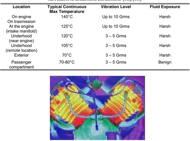
TABLE I.
AUTOMOTIVE OPERATING CONDITIONS [30],[31].
Location Typical Continuous
Max Temperature
Vibration Level Fluid Exposure
On engine
On trasmission 140°C Up to 10 Grms Harsh
At the engine
(intake manifold) 125°C Up to 10 Grms Harsh
Underhood
(near engine) 120°C 3 – 5 Grms Harsh
Underhood
(remote location) 105°C 3 – 5 Grms Harsh
Exterior 70°C 3 – 5 Grms Harsh
Passenger compartment
70-80°C 3 – 5 Grms Benign
Fig. 1. Thermal infrared image of an automobile engine in operation: the cylinders hot zones can be noticed.
5
Because of the very harsh automotive operating environment, electronics modules in a car are often separated from the mechanical systems which they control. Locations like vehicle “firewalls” and fender wells offer the possibility of sinking module-generated heat while reducing exposure to temperatures created by the mechanical systems and allowing some access to airflow available under-the-hood. In this scenario the adoption of proper thermal management systems seems to be the only solution, with the drawbacks represented by the increase in weight and cost.
To keep at minimum power dissipation and up-to-temperature-design-limit, a key component in automotive electronics is the Intelligent Power Switch (IPS), aiming at implementing power driving and management tasks with high efficiency and with integrated protection and diagnostic features. One of the reseach branch carried out within the PhD Program is about the development of an IPS integrating full diagnostic, allowing to detect and to signal extraordinary conditions such as over-current and over-temperature to digital ECUs, by means of a digital interface. Furthermore the IPS developed is configurable to have the capability of driving different and inter-changeable kind of loads efficiently.
1.1.2 Military
The operating conditions in military applications are extremely harsh: high reliability is required in severe conditions, including thermal and mechanical shock vibration, cycling, humidity, corrosive, chemical/biological, and radiation degradation, and altitude changes [1]. The functional lifetime of electronic devices is 20-30 years, more than that of rapidly obsolete consumer electronics, which have an average service life of less than 5 years. For example, missiles are required to be stored for 10 to 20 years in any location in the world and still meet safety and reliability requirements. Avionics must undergo severe changes in temperature, humidity, acceleration, and atmospheric pressure within very short periods of time. As regards aeronautical applications, the gas turbine environment represents one of the harshest ones: sensors are employed for accurate, real time measurements of velocities, pressure, temperatures and concentrations of chemical species, as well as stresses on rotating components. The sensors are required also for the active control of parameters such as, combustion stability, pollution reduction, engine health management, and exhaust profile. The typical environment where they have to operate foresees temperatures up to 2500K and at pressures of 30-40 bar in supersonic combustion areas. Mechanical sensors on rotating components may experience centripetal accelerations up to 75,000 - 100,000g [1].
The trend of military electronics develoment has been governed by performance-based specification for several years. High development cost, high reliability, and high density range, with few parts shared between military and consumer electronics industry. Since the electronics industry has been gradually shifting away from the production of military grade electronic parts, mainly due to high costs and very low volume production, the use of commercial off-the-shelf (COTS) electronic components, which have lower maximum temperature ratings than MIL-SPEC devices, has become more frequent, offering major benefits in the areas of supply and cost. The gradual shift in industry towards all COTS parts, the increasing chip-level temperatures, and the higher circuit density of next generation electronics, together with the need for high reliability and long life cycles of all the parts and materials, has introduced new challenges for harsh environment
6
Fig. 2. Heat dissipation for various events [32].
applications. With miniaturization, the greatest dissipation requirement for high energy military lasers and MEMS devices is expected to be on the order of 100W/cm2 for high performance microprocessors and 1kW/cm2 for high power electronics components with a smaller allowable temperature difference (Fig. 12). Heat dissipation has increased in every field of electronics, and in particular in the military one: as an example the heat flux associated with laser diodes is on the order of several kW/cm2 nowadays, comparable to the heat flux associated with ballistic missile entry.
1.1.3 Space
Space missions represent probably the harshest environment for electronic equipment: an interesting example is the Deep Space 2 (DS2) mission [1]. DS2 mission was constituted of two spacecraft systems with the aim to penetrate below the surface of Mars; the mission started in January in 1999 but unfortunately failed, indeed no transmission was received after the impact on the planet surface. The operating conditions in space missions are indeed extremely severe in temperature, pressure, radiation. Landed missions to the planet Venus [60], for instance, have to deal with an atmospheric ambient of 93 bars and 740K, with the presence of acid rain due to sulfuric acid clouds in the Venusian upper atmosphere. A third example is Europa, a moon of Jupiter, considered an interesting space exploration target due to the possible presence of a sub-surface ocean. The environment that electronic equipment should cope with, includes a combination of cryogenic temperature (100K) and intense radiation from being within Jupiter’s magnetosphere. Estimates of the surface radiation exposure exceed 107 rad/month of mission life [61].
The environmental temperature in many space missions is significantly below the range for which conventional commercial-off-the-shels electronics is designed. Spacecraft operating in the cold environment of such deep space missions carry a large number of radioisotope or other heating units in order to maintain the
7
TABLE II
TYPICAL OPERATIONAL TEMPERATURES FOR UNHEATED SPACECRAFT [62].
Planet Spacecraft Temperature Mercury 175°C Venus 55°C Earth 6°C Mars -47°C Jupiter -151°C Saturn -183°C Uranus -209°C Neptune -222°C
surrounding temperature of the on-board electronics at approximately 20 °C. Indeed, as can be noticed in Table II, the operational temperatures for unheated spacecraft in the environment of outer planets would be not compatible with solid-state eletronic devices.
The primary power source on board of a satellite are the solar panels. When the panels are exposed to the sun they provide power to the load and to charge the on board batteries that are discharged when the satellite is in eclipse. The accumulators provide DC voltages in the 20 to 50V range (Power Bus), which supply few KW of power. Besides high power electronic unit (for Radar, Electrical Propulsion, etc.) the satellite is plenty of low power multi-output DC/DC converters, which convert the input voltage levels into a number of different output voltages from 2.2V up to few KV. To be taken into consideration that a typical "space" DC/DC converter is manufactured in few pieces so the minimisation of the cost design is necessary, unlike mass production where the recurring cost reduction is the main target. Flexibility is the second important aspect of these components: indeed, the DC/DC converters on-board supply several different kind of loads, digital, analogue, RF with very low noise requirement, scientific instrument and so on. Additional aspects to be considered in space applications are:
• The thermal management design is complicated by the fact that in space missions there is no air and therefore no convective heat transfer. Only conductive path are available for cooling the system to the satellite wall. Heat is then radiated to the surrounding space.
• The high vibration level during the launch, stress electrical components from a mechanical point of view. Heavier parts have therefore to be glued to the printed circuit board or to a mechanical frame.
• Obviously, reliability is a key factor in space application: that involves component de-rating and a continuous inspection during manufacturing phases. This means that every soldering and bonding have to be accessible and therefore often limiting the integration of different parts.
8
Fig. 3. Temperature range for various electronics applications.
• Radiation particles, as heavy ions, protons, electrons and γ ray continuously bombard electronic devices during flight operation. Shielding is sometime requested but it should be limited to sensitive items because it is made by high density materials.
• Redundancy is another key element in designing electronics for space applications. In case of failure of the nominal part, its redundant counterpart allows to operate nominally.
• Conducted emission/susceptibility requirements change for different satellites even though the Mil-STD461 is a common background. That makes difficult to define a standard EMI filter.
1.2 HARSH ENVIRONMENTS: REQUIREMENTS AND
CONSTRAINTS
1.2.1 Operating temperature
A great deal of work has been spent over the years on the development of highly effective cooling systems for the heat removal in power electronics, optoelectronics, and telecommunication systems. Yet, electronic components and systems capable of high-temperature operation allow designers to eliminate, or at least minimize, the high cost for cooling systems currently required to protect electronics from extreme environments. In the automotive, for instance, the IPS are currently largely employed to drive the different loads placed on each vehicle. They aim at implementing power driving and management tasks with high efficiency and with integrated protection and diagnostic features.
In a typical electronic system operating in high temperature environment, the heat removal from the chip may require the use of several heat transfer mechanisms to transport heat to the coolant or the surrounding environment. Three basic heat transfer modes exist: conduction, convection and radiation. Thermal management techniques can be classified as either passive, active, or a combination of the two (hybrid).
9
Fig. 4. Output characteristics of a power mosfet, by varying the operating temperature.
The passive modes, relatively reliable and simple to implement, are however performance-limited for many high power applications. The main passive thermal management techniques are:
• Conduction (metal spreader, interface materials, adhesives, pads, pastes, epoxy bond)
• Natural convection (finned heat sinks, ventilation slots, liquid immersion cooling)
• Radiation (paints, coatings, mechanical surface treatments)
• Phase change (phase change materials, heat pipes, thermosyphons, vapor phase chambers).
Active thermal management techniques, requiring input power, provide increased performance/capacity, but also:
• Reduced reliability and added complexity. The essential active techniques include:
• Forced convection (fans, nozzles)
• Pumped loops (heat exchangers, cold plates, jet/spray)
• Refrigerators & coolers (vapor-compression, vortex,thermoacoustic, thermoelectric/Peltier)
In the applications where conventional thermal management is employed, “smart cooling systems” integrating control loops consisting of the control chip, temperature sensors, and heat pumps, guarantee longer lifetime of the devices. In general, traditional air cooling semiconductor devices have been partly replaced by methods using liquid coolants. A classical example is power electronics where several switching components with variable frequency and voltage, require intensive cooling: in these cases, air cooling does not allow to cope with the high heat flux densities to be removed and therefore liquid coolants are used to handle high power losses, since the heat transfer coefficients from the component to the coolant are up to two orders of magnitude higher.
The temperature sensitivity of the electrical components parameters, needs to be carefully considered in the design of electronic systems operating in harsh environment. In [62] a deep analysis of semiconductor devices, capacitors, magnetic cores and pulse-width modulation chips has been performed. As reported in Fig. 4, there is a strong influence of operating temperature on family curves of drain current (ID) versus drain-to-source voltage (VDS) at various gate-source
10
TABLE III
IMPACT OF TEMPERATURE ON THE ELECTRICAL BEHAVIOR OF SENSORS AND SEMICONDUCTOR DEVICES [63].
Device Effect of high temperature
Thermistor Number of charge carriers and conductivity increases Piezoresistive sensors
with pn-insulation of the piezoresistors
Sensitivity decreases Junction leakage current increases Schottky diodes Forward voltage drop decreases
Reverse current increases with T2 Pn-diode Voltage drop in forward direction decreases
Leakage current increases exponentially Bipolar transistor Base-emitter voltage decreases at collector current
Current amplification increases with Tx (1<x<2) JFET Channel mobility decreases with T3/2
Pich-off voltage increases
MESFET Similar to JFET
MOSFET Channel mobility decreases with T3/2
Leakage current of pn-junctions increases exponentially Threshold voltage decreases
voltages (VGS). The first deviation noticeable with the temperature is the downward
shift of the switching curves, for a given gate voltage, as the temperature is decreased. This behaviour is due to the increase in the gate threshold voltage with decreasing temperature. The second deviation is the increase in slope of the switching curves as the temperature is lowered. This trend is primarily caused by the decrease in the on-state resistance with decreasing temperature.
1.2.2 Particle radiation
Particle radiations represent a very critical aspect of electronic employment both in Space and High Energy Physics applications. Radiation effects are traceable to the interaction of radiation (photons, particles) with the materials composing the electronics. Energy can be released by the photon/particle via ionization or nonionization mechanisms. Depending on the operating environment different kind of radiation can be present:
• Protons and other hydrogen nuclei stripped of their electrons • Positively charged alpha particles (α)
• Helium ions at high energy levels
• HZE ions, whose nuclei are heavier than helium • Positively or negatively charged beta particles (β+ or β-) • Photons (X, γ)
• Neutrons • Neutrinos
11
• Hadrons
The energy released by photon/particle leads to different phenomena, via ionization or non-ionization mechanisms. Photons generate small density of e-h pairs, while heavy ions can cause large density of electron-hole pairs. Protons and neutron create high density charges for direct ionization, due to possible nuclear interaction of the particle with the semiconductor lattice. Finally, hadrons can lead to dislocation of atoms from lattice.
Two possible effects have to be distingushed in radiation environment: cumulative effects or single event effects.
Cumulative effects are gradual effects taking place during the whole lifetime of the electronics exposed in a radiation environment. A device sensitive to TID or displacement damage will exhibit failure in a radiation environment when the accumulated TID (or particle fluence) has reached its tolerance limits. The TID is the measurement of the dose, that is the energy, deposited in the material of interest by radiation in the form of ionization energy. The ionization dose is deposited by particles passing through the materials constituting the electronic devices. This happens during the whole time the device is exposed to radiation. The level of radiation hardness against TID depends on the final application of the circuit, i.e. for an an interplanetary mission the TID required for the components are in the range of MRad [64], while in the case of low orbital satellites the required TID is ~100kRad. In HEP experiments such as SLHC the required TID hardness is up to 100 Mrad. In the LHC environment, ionization effects are induced by the ionization energy deposited by charged hadrons, electrons, gammas and neutrons (even though the last two are not directly ionizing, they can induce ionizing energy depositions).
The most important effect of TID is the trapping of charges within the oxide, mainly positive. The trapping of the charges is bigger in the transition region from gate oxide to field oxide, known as peak region in old technologies, and substituted by the shallow trench isolation (STI) in the sub-micron technologies. The accumulation of positive charges at the borders of the linear transistors produces the leakage current on the NMOS transistors in cut-off mode, while PMOS transistors are less sensitive to the accumulation of this charge. The use of Edge Less Transistors (ELTs) avoids the transition region between the drain and source, and eliminates the leakage between them.
Single Event Effects (SEE) are instead due to the energy deposited by one single particle in the electronic device. Therefore, they can happen in any moment, and their probability is expressed in terms of cross-section. A device sensitive to SEE can exhibit failure at any moment since the beginning of its operation in a radiation environment.
SEE can be classified as:
• Transient: spurious signals propagating in the circuit (Single Event Transient, SET).
• Static: errors overwriting information stored by the circuit (Single Event Upset, SEU).
• Permanent: destructive errors cause irreversible effects such as the latch-up of the device (Single Event Latchup, SEL) or dielectric breakdown of the gate oxide (Single Event Gate Rupture, SEGR).
12
SEE errors are related to the pass of a high energy particle that releases energy creating hole-electron pairs: the charge is collected in noded of the circuit causing a transitory spike (SET), the flip of the value (SEU), or the ignition of the latch-up effect related to the PNPN parasitic structure of the technology.
Transient errors are frequent in combinational logic, generating asynchronous signals, that can propagate through the circuit during one clock cycle and also sometimes propagate to a latch and become static.
Static errors can be corrected by outside control, by overwriting information stored in the circuit, but a rewrite or power cycle can correct the error with no permanent damage.
Permanent or hard errors are those leading to a permanent error, which can be the failure of the whole circuit. They cannot be recovered unless detected at their very beginning in some cases (as for Latchup). In that case, it is possible to interrupt the destructive mechanism and bring back the circuit to functionality.
13
2
HIGH ENERGY PHYSICS EXPERIMENTS: DEVELOPMENT,
DESIGN AND TESTING FLOW OF AN INTEGRATED CIRCUIT
2.1 Introduction
Particle physics is the branch of physics that studies the most basic constituents of matter and their interactions. Modern particle physics research is focused on subatomic particles, i.e. particles with /dimensions and mass smaller than atoms, including atomic constituents such as electrons, protons and neutrons and particles produced by radiative and scattering processes, such as photons, neutrinos and muons. Since many elementary particles do not occur under normal circumstances in nature, to allow their study they are created and detected by means of high energy collisions of other particles in particle accelerators: therefore, particle physics is often referred to as High Energy Physics (HEP).
The main instruments for HEP are particle accelerators, large and complex machines that produce beams of particles and provide them with the high energies needed for HEP experiments. Accelerators typically employ electric fields to increase kinetic energy of particles and magnetic fields to bend and focus the beam, which is then collided against a fixed target or with another particle beam: the high energy collision produces the new particles and events that must be detected and studied. Beside the use in particle physics, the applications of accelerators nowadays span from industry (e.g. ion implantation in electronic circuits) to medicine (radiotherapy), with different ranges of energy for the different fields application. Current accelerators for HEP work in the GeV and TeV energy range (referring to the energy provided to particle beams) and typically treat beams of electrons, hadrons and heavy atomic nuclei; the structure can be linear (LINAC, LINear ACcelerator), with the particle beam traveling from one end to the other and colliding against a fixed target, or circular (cyclotrons, synchrotrons), with the beams traveling repeatedly around a ring, gaining more energy at every loop and colliding with other beams running in opposite direction
HEP experiments thus consist in colliding particle beams in accelerators and studying the results of the collisions using particle detectors that surround the interaction point. Particle detectors are devices used to track and identify high-energy particles produced in collisions, also measuring their attributes like momentum, charge and mass. A particle detector is typically made up of different layers of sub-detectors, each specialized in revealing and measuring different particles and properties of particles. To help identify the particles produced in the collisions, the detector usually includes a magnetic field that bends the path of charged particles: from the curvature of the path, it is possible to calculate the particle momentum which helps in identifying its type. Particles with very high momentum travel in almost straight lines, whereas those with low momentum move forward in tight spirals.
To record and analyze events produced by collisions in an experiment, information about particles detected by sensors in the detector are converted into electric signals, which are then collected by dedicated electronic components embedded in the detector and located in close contact with the sensors themselves: these devices, usually called Front-End (FE) electronics, deal with the proper conditioning of signals (e.g. amplification, shaping, buffering, analog to digital
14
conversion) and their transmission to remote data acquisition systems that perform data analysis and storage. The number of interactions per second is very high (a typical order of magnitude is billions of particle interactions per second); a measure of collision rate is the so-called luminosity, which is usually expressed in cm-2·s-1 and for a two-beam collider is defined as the number of particles per second in one beam multiplied by the number of collisions per unit area in the other beam at the crossing point. Collision rates of this order of magnitude produce amounts of raw data that range from tens of terabyte to a petabyte per second, which is beyond the possibility of any data acquisition and storage system. Therefore, since the interesting events are a very small fraction of the total, the total amount of data is filtered by means of a trigger system: raw data are temporarily buffered in the FE electronics while a small amount of key information is used by trigger processors to perform a fast, approximate calculation and identify significant events: the result of this processing is a trigger signal that is sent back to FE electronics to command a data readout, i.e. the transferring of a selection of the buffered data towards the remote system. This way, the amount of data to be transferred is reduced to rates that can be handled by the readout system (a typical order of magnitude is hundreds of MB/s from each FE device), and only the interesting events are selected.
HEP experiments constitute a very challenging application for electronics, since the equipment must deal with large amounts of data and high data rates, with tight timing and data integrity constraints and operate in an environment that is intrinsically hostile due to the high levels of radiation. In particular, electronic devices and systems employed in HEP experiments must tolerate high levels of ionizing radiations and the associated cumulative effects and SEE.
The LHC, the well known facility at the European Organization for Nuclear Research (CERN), located near Geneva in Switzerland is the world’s most energetic accelerator. It currently allows to produce roduce proton–proton collisions at a centre-of-mass energy of 14 TeV and a luminosity of up to 1034 cm–2·s–1, yet
an upgrade of its performance will be gained within the sLHC project (super LHC), which aims for a tenfold increase in luminosity for 14 TeV proton–proton collisions, achieved through the successive implementation of several new elements and technical improvements that are scheduled for 2013–2018. The final luminosity will be 1035 cm−2·s−1, providing a better chance to see rare processes and improving
statistically marginal measurements.
Obviously, such upgrade in terms of luminosity will lead to complex challenges that have to be developed, not only in radiation hard detectors but in powering, cooling, thermal management and integration engineering. As radiation damage scales with integrated luminosity, the radiation environment inside the detector will increase. Besides the previous highlighted point, the small size represents a very critical aspect to be taken into account for electronic devices working in HEP experiments: the space available for devices and cabling inside a particle detector is usually very limited due to the large amount of different components (readout and control systems, cooling systems, mechanical structures and so on) that must be integrated in a small area around the interaction point; in addition, bulky equipments are undesired because any non-sensor material interferes with the measure by deflecting and absorbing the particles that must be detected (the amount of material surrounding the interaction point, characterized with the
15
radiation thickness of each component/layer, is usually referred to as material budget).
Another important requirement of electronic devices for HEP experiments is low power dissipation: due to the high concentration of electronic equipment inside the detector, power density is a major issue because it dictates the cooling requirements; cooling systems represent a critical aspect in HEP experiments because they complicate the material budget and the mechanical requirements.
2.2
DAQ/TTC SYSTEMS FOR HEP EXPERIMENTS
HEP experiments have non-homogeneous latency and bandwidth requirements for data transfers between FE electronics and remote trigger processors and control/data acquisition systems. In most of the past and current HEP experiments, e.g. [2-6], different custom protocols have been used to distribute Timing, Trigger and Control (TTC) signals and to perform the Data Acquisition (DAQ) within the same experiment and, sometimes, within the same detector.
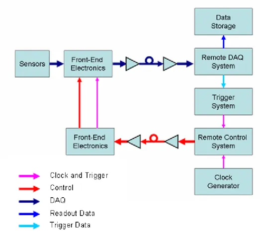
A typical control and readout system for a HEP experiment can be schematized as in Fig. 6.
Fig. 6. Typical architecture of the control and readout system for a HEP experiment.
16
Signals generated by the interaction with sensors of particles produced in the beam collisions are handled by FE electronics embedded in the detectors and transferred to remote DAQ systems, located far away from the experiment area to keep them in an environment that is free from the intensive levels of radiation that are present in the proximities of the interaction point. Typically, the transfer is carried out by means of electrical links for a first stretch inside the detector, and then through optical links that allow to cover the long distances (hundred of meters) from the experiment area to the remote DAQ system, and provide the large bandwidth needed (up to tens of Gbit/s). A subset of the transferred data is used to perform trigger calculation, and the generated trigger command is sent back to FE electronics along with timing (clock) and control signals by a remote control system, also called TTC system, that manages the configuration and monitoring processes in the FE electronics.
In future experiments, the use of “standard” and flexible protocols will contribute to meet the mentioned requirements about latency and bandiwidth, with a reasonable impact on the development and production costs and with a reduction of the complexity of the control and readout systems (hardware, firmware and software). The GigaBit Transceiver (GBT) project represents an example of what indicated above, aiming at the fulfillment of the high data rates and radiation doses foreseen in the physics experiments of the future upgrade of the LHC accelerator, the SLHC [19-22]. Indeed, because of the high beam luminosity planned for the SLHC, in this scenario the data rate expected is very high and, besides that, links and electronic components need to be capable of sustaining high radiation doses. The GBT ASICs address this issue implementing a radiation-hard bi-directional 4.8 Gb/s optical fibre link between the counting room and the experiments. In particular, the goal of the GBT project is to produce the electrical components of a radiation hard optical link, following the scheme described hereafter: one half of the system resides on the detector and hence in a radiation environment, therefore requiring custom electronics. The other half of the system is free from radiation and can use commercially-available components. Optical data transmission is via a system of opto-electronics components produced by the Versatile Link project. The architecture incorporates timing and trigger signals, detector data and slow controls all into one physical link, hence providing an economic solution for all data transmission in a particle physics experiment.
The FF-LYNX project, one of the research branch studied during the PhD program [8], shares the same goal with the GBT project, without focusing on specific physics experiments having fully defined bandwidth and radiation tolerance requirements. FF-LYNX aims at the definition of a fast and flexible protocol that allows the use of the same physical serial links for the transmission of TTC signals and the DAQ and the development of a full set of Transmitter (TX) and Receiver (RX) interfaces to optical and electrical serial links implementing this protocol. The main feature of the FF-LYNX project is its feasibility that makes it suitable for different HEP experiments, e.g. CMS End-Cap Muon detector in [23], as well as medical physics applications, e.g. block detector for Positron Emission Tomography (PET) in [24].
17
Fig.7. FF-LYNX serial data stream, fast and reference clock in the three speed options: the first two bits of each cycle are assigned to the THS channel, the
remaining bit to the FRM channel.
2.3 DESIGN FLOW OF ELECTRONIC SYSTEMS FOR HEP
APPLICATIONS
The methodology followed during the FF-LYNX project represents a case study of development flow for electronic systems and devices operating in harsh environment, such as HEP experiments.
The entire methodology has included design activities and successive phases of verification steps, in order to validate the results obtained in each stage. A key step characteristic of this methodology has been the use of a high-level software model of the link where the proposed FF-LYNX protocol would have been applied, allowing the comparison of different choices about the various aspects of the protocol itself on the basis of conveniently chosen cost functions and figures of merit (e.g. bandwidth efficiency, robustness to errors, etc.).
The project work flow is reported in Fig. 8; the main phases of the flow are hereafter described:
• Analysis of the requirements of the future TTC and DAQ systems: within this starting phase it has been performed an evaluation of trigger and data rates in different luminosity conditions and with different sensor geometries (e.g.: pixel and strips with different sizes) and detector architecture (e.g.: number of detector layers and distance of the layers from the interaction point).
• Protocol definition: starting from the detailed requirement analysis, the second stage of the activity is the definition of the FF-LYNX protocol in a first, tentative version to be submitted to successive verification, and open to refinements following suggestions and requests from FF-LYNX collaborators in the field of HEP experiments (physicists and engineers involved in the design of detectors). This first version of the protocol has been defined focusing on the requirements about data rate, trigger latency and error robustness by means
18
of a mix of custom and standard solutions typical of the data-link layer of the ISO/OSI model.
• Validation of the protocol in a high-level simulation environment: the cost metrics have been integrated within an Integrated Simulation Environment (ISE), based on System-C language [21]. This high-level software simulation environment has modelled the transmitter and receiver interfaces, implementing the defined protocol, and a surrounding test bench providing the expected stimuli and measuring various aspects of the link performance. This environment has been realized in System-C, offering a highly configurable model of the link in order to allow the test, during the phases of protocol definition and refinements, of different versions of the protocol. To validate the protocol and allow comparisons between different versions, the basic task of the high-level simulator has been the evaluation of specific cost functions and figures of merit (e.g. bandwidth efficiency, data loss rate, data latency) that has been defined on the basis of system requirements; furthermore, by evaluating these parameters, the high-level simulator has also offered valuable information about hardware aspects of the interfaces, such as optimum size of buffers.
• Definition of the interfaces architecture: after the protocol validation phase, the architecture of the hardware interfaces implementing the first version of the protocol has been defined, following indications from the high-level simulation phase. The overall architecture of the transmitter and receiver interfaces has been divided into functional blocks in order to simplify the implementation and to allow the separate verification, in the successive HDL simulation phase, of the correctness of each sub-function.
• VHDL modeling and simulation: following the definition of their architecture, a model of the interfaces using a Hardware Description Language (HDL) has been created for functional simulation and successive synthesis. This model has been built in a highly-parameterized form in order to allow quick changes to follow indications coming from the high-level simulator. Each block of the architecture has been separately modelled and tested in a specific test bench through functional simulation to verify its functionality, so to progressively build an overall model that was verified in all its parts. The final verification phase has been focused on the the complete transmitter-receiver model by means of a test bench including emulators of the transmitting and receiving hosts to verify the overall functionality of the system.
• FPGA prototype development: a phase of FPGA-based emulation has been foreseen, to provide additional verification of the system functionality (especially about the aspects that are difficult to assess in the software simulator, due to excessive simulation time: i.e. the evaluation of the effect of transmission errors on data integrity with realistic bit error rates – in the order of 10-9 or less – has required few days of simulation) and to evaluate different solutions for the physical layer. The HDL models of the interfaces have been synthesized on an FPGA along with the model of a surrounding test system that has provided test vectors to the interfaces model and recorded the test results.
19
• Test chip design: the design and implentation of a test chip has completed the overall development flow. The test-chip FF-TC1 has embedded the transmitter and receiver interfaces and the same test bench architecture previously synthesized on the FPGA emulator. This phase has required the application of Radiation By-Design Hardening techniques, in order to make the test chip suitable for the radiation dose foreseen in the operating environment. In order to deeply evaluated the functioning of the interfaces, as regards both timing and radiation requirements, an accurate validation flow has also been performed.
20
2.4
THE FF-LYNX PROTOCOL
The FF-LYNX protocol is a “double wire” serial, packet based protocol with data structure independent w.r.t. data type (e.g.: configuration data, monitoring data, commands, row data). It has been developed with the aim of offering a high degree of flexibility with respect to various parameters and aspects of the transmission systems, such as the data rate and the data format. Regarding data rate, the protocol is proposed in different versions with different values of the data transmission speed, chosen as multiple of the reference clock frequency of the application. The three speed options are: 4xF, 8xF and 16xF (F = reference clock frequency) that, in the LHC scenario (F = 40 MHz), correspond to 160, 320 and 640 Mbps respectively. The reference clock used in the FE electronics is recovered in the destination devices from the high speed clock used in the transmission of the serial stream and its synchronization with the reference clock in the source device is guaranteed by the protocol itself.
The integrated distribution of TTC signals and DAQ represents another key feature of the FF-LYNX protocol, making it suitable both for the Up-Links from the FE electronics to the remote acquisition and elaboration system, and for the Down-Links from the trigger processor and the central control system to the FE electronics. This is obtained by multiplexing two channels in the time domain: the THS channel used for Triggers, frame Headers and Synchronization patterns and the FRM channel for data Frames. The THS channel employs the first two bits after the rising edge of the reference clock for the transmission of triggers, headers and synchronization commands, encoded with 6-bit patterns, transmitted in three consecutive cycles of the reference clock.
Triggers have higher priority with respect to frame headers and synchronization commands, that can be transmitted only when the THS channel is not used for triggers for at least three consecutive clock cycles. This choice is compatible with the minimum number (three) of clock cycles between two consecutive triggers foreseen for the upgrades of the LHC experiments and it prevents effects of single bit flips in the data stream on the pattern detection and on the correct reconstruction of its timing.
The remaining 2, 6 or 14 bits (FRM channel) are used for data frames tagged by frame headers transmitted in the THS channel. Such strategy allows the transmission of triggers to the FE circuits, as well as user data (configuration/control commands) on the same physical link.
The data format is transparent with respect to the data type (e.g.: commands in the Down-Link toward the detector or data from Front-End circuits in the Up-Link from the detector): the protocol transfers user information from the transmitter to the receiver without introducing any structure in the payload, thus accepting any kind of data format. Data frames in the FRM channel are tagged by frame headers transmitted in the THS channel and have the general structure shown in Fig. 9 and described below:
• Frame Descriptor (7 bits, encoded with Hamming in 12 bits) This field contains the following frame information:
21
1) Frame_Length (4 bits) → it indicates the length of the frame, including the Payload and an optional 16-bit field (Label) between the Frame Descriptor and the Payload; it is expressed in number of 16-bit words (1→16);
2) Label_On (1 bit) → it specifies whether the optional Label between the Frame Descriptor and the Payload is present or not; if a data packet with Label is fragmented in multiple frames, the Label is attached to the first frame only;
3) Data_Type (1 bit) → it specifies the data type: (e.g.: ”raw” data generated after the reception of a L1 trigger or configuration or monitoring data, generated after the reception of a command);
4) Last_Frame (1 bit) → it indicates, in the transmission of a data packet fragmented in multiple frames, whether the current frame is the last one of the sequence of frames or not.
• Label (16-bits)
The Label can follow the Field Descriptor and precede the Payload. In the Down-Link it can be used to transmit destination address and operation code of commands (e.g.: reset, write/read access to registers). Data frames generated by read commands as well as empty data frames generated by write commands and used as acknowledgements can keep the Label of the original command frame. In the Up-Link the label can be used to transmit the time stamp or the trigger number associated to the transmitted “raw” data. • Payload (N x 16-bit words)
Different data types can be transmitted in the payload: configuration or monitoring data generated after the execution of a command, “raw” data generated after the reception of a L1 trigger, “trigger” data to be used in embedded or remote processors for the generation of the L1 Trigger. Long data packets can be fragmented into multiple data frames and a “Last Frame” flag in the Frame Descriptor identifies the last one. The maximum length of the data frames is determined by the depth of the input/output buffers in the transmitter and receiver interfaces.
• CRC (8 bits)
The Cycle Redundancy Check (CRC) can be optionally applied to the Payload and the Label to increase robustness against transmission errors
22
Fig.10. Possible up-link data stream in the 8xF link speed option: variable and fixed latency frames, carrying hit information, are transmitted through the THS and FRM
channel.
The robustness of critical information against transmission errors is ensured by means of Hamming codes and custom encoding techniques. The custom 6-bit encoding applied to the THS channel allows the correct recognition of the transmitted commands and the reconstruction of their exact timing, while the Hamming code, used for the Frame Descriptors, corrects single bit-flips and detects burst errors, performing Single Error Correction (SEC) and Double Error Detection (DED).
Another important feature of the FF-LYNX protocol is represented by the easy coupling of the interfaces with the core of the host circuits, indeed interfaces to electrical serial links are provided with both serial and parallel ports implementing a very simple handshaking protocol with the core of the host circuits.
The most innovative element offered by the FF-LYNX protocol is the flexibility with respect to the latency of the frames: in addition to Variable Latency Frames (VLF), having no constraints in terms of latency, the transmission of Fixed Latency Frames (FLF), with fixed and low latency, is supported. This feature broadens the range of applications of the FF-LYNX protocol: an example is its applicability to the data transfers from FE electronics to embedded or remote trigger processors that will use “trigger” data in the generation of the Level 1 Trigger (L1T). The “trigger” data, as hit coordinates to be used for track finding or hit timing, can be encapsulated in FL frames and transmitted from the FE circuits to a remote trigger processor through the Up-Links. The transmission of the frame starts when
23
Fig. 11. Possible structure of data frames (fixed length) in the FF-LYNX protocol “trigger” data to be used in the L1T Trigger generation are detected in the FE circuits. Frame length and link speed are fixed taking into account the number of hits that can occur during the clock cycles involved in the data transfer.
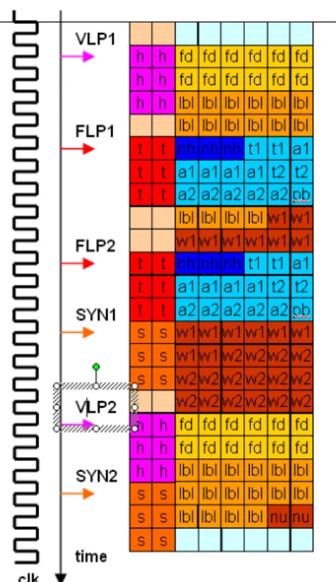
In Fig. 10 the possible structure of a 3-clock-cycle-long data frame is shown: 2 bits are used to identify the timing of the hits and 5 bits to encode the hit address (e.g.: the address of the cluster where the hit occurred in a FE ASIC with 128 channels grouped in clusters of 4 channel each). With a link speed of 8xF, 18 bits are available in the FRM channel to encode one or two hits: 1 bit encoded with Hamming in 3 bits is used to specify the number of transmitted hits, while the last available bit is used for parity check. Different possible configurations w.r.t. link speed and frame length have been simulated in order to evaluate their efficiency in the transmission of trigger data: values of the Trigger Transmission Efficiency (TTE) for different values of Link Speed (LS), frame length expressed in clock cycles (NC) and maximum number of transmitted hits (NH) are summarized in Table I. These results have been obtained assuming a Poisson distribution for hits (0.125 hits/clock cycle) and hits generated by one FE circuit in simulations with LS = 8xF and by four FE circuits in simulations with LS = 16xF.
A possible data stream in the Up-Link from the detector is shown in Fig. 12: two FLF (FLP1 and FLP2) interrupt the transmission of a VLF VLP1 that is then regularly completed (e.g: VLP1 = “raw” data generated after the reception of a L1 trigger → lbl = time stamp, w1 = 1st hit, w2 = 2nd hit). A second empty variable
latency packet (VLP2) follows (e.g.: VLP2 = acknowledge of a command received through the Down-Link).
TABLE IV
TRIGGER TRANSMISSION EFFICIENCY.
LS NC NC TTE
8xF 3 2 96.57%
8xF 5 3 98.53%
16xF 4 7 97.29%
24
Fig. 12. Possible data stream in the Up-Link (h=frame header, t=trigger, s=synchronization pattern, fd=frame descriptor, lbl=label, w1 and w2=data words).
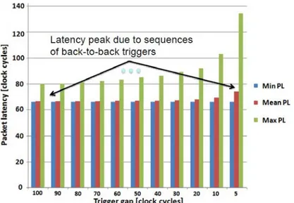
One FLF employs both the THS and the FRM channel for three cycles of the reference clock, transmitting data (i.e.: hit timing and address) associated to a maximum of two hits. The hits can occur at different instants of the three-clock-cycles window, but a possible third hit cannot be handled and, consequently, it is lost. The transmission of a VLF is stopped to allow the transmission of an incoming FLF and re-started after the completion of the transmission of the FLF. The scheduling strategy implemented for the transmission of FLF leads to a latency equal to three reference clock cycles.
The use of the same channel for triggers, fixed and variable latency frames allowed by the FF-LYNX protocol will bring to a significant reduction of the number of physical links and of the overall material budget that affects the detector performance and it is therefore one of the major concerns in the design of the detectors.
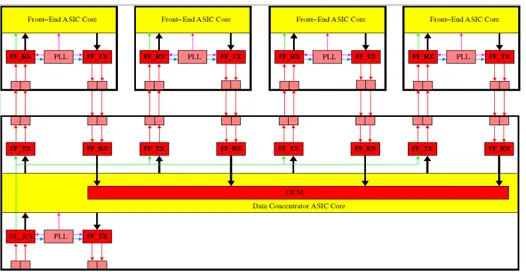
Finally, the flexibility of the protocol with respect to the architecture of the control and readout systems represents an additional strength point, since it is compatible both with “star” and “ring” architectures. A Data Concentrator Module (DCM) can be used in a star topology (see Fig. 13) to merge low speed input data streams from different sources into one high speed output stream.
25
Fig. 13. “Star” architecture of a control and readout system based on FF-LYNX protocol and interfaces.
Fig. 14. “Ring” architecture of a control and readout system based on FF-LYNX protocol and interfaces (redundant connections to prevent effects of single
component failures are included).
In a ring topology (see Fig. 14) the DCM would merge in each node locally generated data with data received from the previous node. Optional “event building” capabilities can be embedded in the data concentrator module: monitoring data generated by the execution of the same command in different Front-End circuits or “raw” data associated to the same trigger can be merged.
2.5 FPGA-BASED
EMULATOR
2.5.1 Emulator system
The functioning of the TX-RX interfaces has been validated through a high-level simulation (ISE) during the first validation phase, and by means of a FPGA-based emulation at the final stage.
26
Fig. 15. Conceptual architecture of the FF-LYNX Emulator.
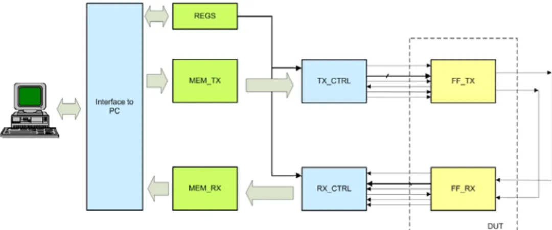
The TX-RX interfaces in the above reported scheme, represent the Device Under Test (DUT). The input signals to the TX interface are provided by the TX Controller (TX_CTRL) that reads test vectors (trigger commands and data packets) stored in a transmitter memory (MEM_TX). An RX Controller (RX_CTRL) reads triggers and data received by the RX interface and writes them into a receiver memory (MEM_RX).
A further comprehension of the emulator functioning is described in Fig. 16. As can be noticed, the TX and RX Controllers are parts of the overall Test Controller, that integrates also TC configuration registers containing test parameters as emulation window duration, number of VLF packets, FLF mode, size of the FLF packets, etc.
The TX controller controls the transmission of FLF packets, trigger or VLF packets at pre-defined clock cycles (TX Time Stamps), whose values are set and stored into a dedicated RAM. The arrival timing of the received triggers and frames is stored in a separate RAM: the contents of the TX-RX Time stamps RAMs are compared to evaluate trigger and the packet latency.
27
Overall, the RAMs embedeed in the FPGA emulator are:
• VLF_TS (Variable Latency Frame Time Stamp) RAM: two 32x4k memories storing the time stamps (TS) associated to VLF data packets transmitted/received to/from FF-LYNX TX/RX interfaces.
• VLF_LEN (Variable Latency Frame Length) RAM: two 8x4k memories storing the length (number of 16bit words) of the VLF data packets transmitted/received to/from FF-LYNX TX/RX interfaces.
• VLF_DW (Variable Latency Frame Data Word) RAM: two 16x32k memories storing the VLF data packets transmitted/received to/from FF-LYNX TX/RX interfaces.
• TRG_TS (Trigger Time Stamp) RAM: two 32x4k memories storing the time stamps associated to triggers or FLF data packets (when they are enabled) transmitted/received to/from FF-LYNX TX/RX interfaces.
• FLF_DW (Fixed Latency Frame Data Word) RAM: two 8x32k memories storing the FLF data packets (when they are enabled) transmitted/received to/from FF-LYNX TX/RX interfaces.
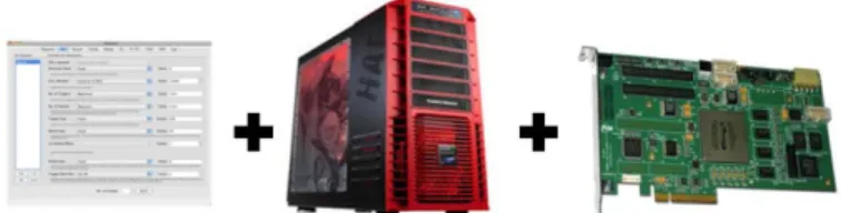
Test vectors are generated by a software application running on a Personal Computer, and then sent to the FPGA-based emulator through the interface module that deals with data exchange between the PC and the Emulator system using the PCIe 2.0 8x bus. The FPGA-platoform is as Altera Stratix II GX FPGA device (EP2SGX130GF1508) [32] housed on a commercial PCIe board (PLDA XpressGXII board) [33]. The Stratix II GX FPGA provides about 133,000 equivalent Logic Elements (LEs), 7 Mbit Total RAM memory, 8 PLLs, 78 LVDS channels, 63 DSP (multipliers and adders) blocks and 20 Transceiver channels with a data rate from 600 Mbps to 6.375 Gbps. The PLDA FPGA development board has been chosen to guarantee a large bandwidth to perform extensive emulations with high data rates (about 1 Gbps) with an acceptable efficiency in terms of emulation time. This board, thanks to the PCIe 2.0 8x bus, can handle a 3.6 GB/s data rate (effective, full duplex).
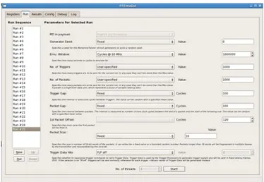
The overall emulation procedure is controlled by a C++ Graphical User Interface (GUI), which configures the configuration registers embedded in the FPGA, provides test patterns to the interface and elaborates the performance figures, by comparing the output signals with the input generated.
Three main blocks constitute the software layer: the PLDA drivers to interface the Host-PC with the PCIe PLDA board, the Data Manager managing the emulator operations, and the GUI (Figure 12) that allows to set the emulation parameters and to display emulation results.
The Data Manager module is a container for all the objects providing data to the GUI, the interface modules using the PLDA API, the stimuli generator (StimGen) and figure-of-merit evaluator (Gauge).
The main blocks making up the Data Manager are:
• EmuRun module that acts as the controller for the emulation runs, by instructing the StimGen to produce the stimuli for the run and to store them in a particular memory area, on the base of a list of parameters set by user (data rate, emulation window duration, packet and trigger rate, number of triggers and packets, etc).
28
• StimGen module that generates the VLF/FLF data packets and the time stamps.
• Gauge block that, according to emulation results, evaluates the Figures of Merit of the emulation run.
Fig. 17. C++ emulator software block diagram.
Fig. 18. GUI controlling the emulator functioning.
Summarizing, the overall emulation system is made up by a software layer, running on a host-PC, where an FPGA development board is mounted: the Fig. 19 Illustrates the global system.
![Fig. 2. Heat dissipation for various events [32].](https://thumb-eu.123doks.com/thumbv2/123dokorg/7626149.116755/14.892.254.643.85.390/fig-heat-dissipation-various-events.webp)