Alma Mater Studiorum · Universit`
a di Bologna
Scuola di Scienze
Dipartimento di Fisica e Astronomia Corso di Laurea Magistrale in Fisica
A PCI Express board designed to interface
with the electronic phase-2 upgrades of the
ATLAS detectors at CERN
Relatore:
Prof. Alessandro Gabrielli
Correlatore:
Dott. Davide Falchieri
Presentata da:
Fabrizio Alfonsi
Abstract
Nei prossimi 10 anni ´e in previsione un aggiornamento radicale dell’acceleratore LHC al CERN finalizzato al raggiungimento di pi´u alti valori di luminosit´a istantanea (oltre 5×1034cm−2s−1) ed integrata (oltre un fattore 10 rispetto a quella attuale).
Conseguente-mente, anche i rilevatori degli esperimenti che lavorano al CERN, cos´ı come i loro sistemi di acquisizione dati, dovranno essere aggiornati per poter gestire un flusso notevolmente maggiore rispetto a quello utilizzato finora. Questa tesi tratta in particolare di una nuova scheda elettronica di lettura, progettata e testata nel laboratorio di elettronica del Dipartimento di Fisica ed Astronomia dell’Universit´a di Bologna e nel laboratorio di elettronica della Sezione INFN (Istituto Nazionale di Fisica Nucleare) di Bologna. Le motivazioni che hanno indotto lo sviluppo della scheda prototipale sono molteplici. Un primo obiettivo da perseguire ´e stato quello di aggiornare la versione attuale delle schede elettroniche di acquisizione dati usate oggi nel Pixel Detector dell’esperimento ATLAS, visto che sono anch’esse sotto la responsabilit´a della sezione INFN di Bologna. Secondari-amente, la scheda (nominata Pixel-ROD) ´e orientata a gestire le esigenze elettroniche che seguiranno l’upgrade di LHC durante la fase 2. La complessit´a del progetto e l’inerzia in-trinseca di una vasta collaborazione come quella di ATLAS, hanno poi indotto lo sviluppo di questo progetto elettronico in largo anticipo rispetto al vero upgrade di fase 2 di LHC, previsto per il 2024. In questo modo saranno anche pi´u facilmente eseguibili eventuali aggiornamenti tecnologici in corso d’opera, senza dover riprogettare da zero un sistema di acquisizione dati completo. Per le esigenze appena descritte, dal punto di vista hard-ware la scheda ´e stata dotata sia di moderni e veloci sistemi di interfacciamento, come la connessione PCI Express, sia di sistemi gi´a ampiamente collaudati, come la connessione Gigabit ethernet. Parallelamente a ci´o, la scheda gestisce sistemi di trasmissione dati ad alta velocit´a sia su fibra ottica che tramite connessione elettrica su linee differenziali. La Pixel-ROD si basa su un’architettura gestita da due dispositivi programmabili di tipo FPGA. La prima, una Master FPGA (XILINX Zynq) ha il compito di controllo generale della scheda stessa mentre la seconda, una Slave FPGA (XILINX Kintex) ha il compito di gestire il flusso dei dati. La versatilit´a di connessione e la capacit´a di calcolo della scheda ´e potenziata da un processore fisico ARM, incluso nella Master FPGA, in grado di facilitare l’interfacciamento anche con altri progetti elettronici sviluppati all’interno della collaborazione ATLAS, che utilizzino linguaggi di programmazione standard non espressamente orientati all’elettronica. Questa tesi ´e composta da una parte introdut-tiva di presentazione dell’acceleratore al CERN, LHC, e dell’esperimento ATLAS. Poi segue una parte descrittiva del progetto e del funzionamento dell’attuale Pixel Detec-tor di ATLAS. Successivamente la tesi descrive un possibile sistema di acquisizione dati aggiornato in visione della fase 2 di LHC, per esempio ancora relativamente al Pixel De-tector, basato su schede come la Pixel-ROD. In questa parte sono descritti in dettaglio il progetto della scheda, il suo funzionamento e i test effettuati in laboratorio. I test in particolare riguardano il contributo personale che il sottoscritto ha fornito al progetto
ed alla collaborazione. Si descrivono anche i primi test congiunti, nel laboratorio del NIKHEF ad Amsterdam, con altri prototipi elettronici sviluppati dalla collaborazione internazionale ATLAS. I test sono stati eseguiti utilizzando un protocollo denominato Aurora 64b/66b, previsto nel panorama dei protocolli di comunicazione che verranno utilizzati nel futuro sistema di acquisizione dati del Pixel Detector, ed un protocollo de-nominato GBT (GigaBit Transmission), molto utilizzato anche adesso negli esperimenti al CERN. Infine la tesi propone una presentazione degli scenari di applicazione futura.
Contents
1 ATLAS Experiment 6 1.1 LHC Accelerator . . . 6 1.2 LHC Experiments . . . 8 1.3 ATLAS Detector . . . 9 1.4 ATLAS Physics . . . 91.5 ATLAS Coordinate System . . . 9
1.6 ATLAS Composition . . . 11 1.6.1 Inner Detector . . . 11 1.6.2 Calorimeter . . . 14 1.6.3 Muon Spectrometer . . . 14 1.6.4 Magnetic System . . . 15 1.7 ATLAS Trigger . . . 17 2 Pixel Detector 19 2.1 Modules . . . 20 2.2 Sensor . . . 22 2.3 IBL . . . 23
2.3.1 IBL Sensor and Modules . . . 23
2.3.2 FE-I4 . . . 24 2.4 BOC-ROD System . . . 28 2.5 BOC-ROD Comunication . . . 29 2.6 IBL-BOC . . . 29 2.6.1 BCF . . . 29 2.6.2 BMFs . . . 30 2.7 IBL-ROD . . . 32 2.7.1 ROD Controller . . . 32 2.7.2 Spartan Slave . . . 33 2.7.3 PRM . . . 35 2.7.4 SBC . . . 35 2.7.5 Lattice PLL . . . 35 2.7.6 S-Link . . . 36
2.7.7 TIM . . . 36 3 Pixel-ROD 38 3.1 Pixel-ROD . . . 40 3.1.1 FPGAs . . . 40 3.1.2 Memory . . . 42 3.1.3 Internal Bus . . . 43 3.1.4 I/O . . . 43 3.1.5 Components . . . 44
3.1.6 Switches, Bottoms and LEDs . . . 44
3.1.7 Power Supply System . . . 44
4 Preliminary Tests 46 4.1 Power On . . . 46
4.2 System Clock and Internal Bus Test . . . 48
4.3 FPGAs RAM Tests . . . 48
4.4 Ethernet Ports Tests . . . 52
4.5 I2C LVDS Oscillator Tests . . . 53
4.6 Fast Links Tests . . . 55
4.7 PCI Express Test . . . 58
5 Implementation 59 5.1 Aurora 64b/66b Connection . . . 59
5.2 GBT Protocol . . . 61
6 Future Developments and Conclusion 63 7 Appendix 65 7.1 FPGA . . . 65
7.2 JTAG . . . 67
7.2.1 Boundary Scan . . . 67
7.2.2 Registers . . . 69
7.2.3 Test Access Port Controller . . . 69
7.2.4 Boundary Scan Instructions . . . 69
7.3 AXI4 . . . 71
7.4 IBERT LogiCore IP . . . 73
7.5 Aurora Protocol . . . 75
7.5.1 Data Transmission and Reception . . . 75
7.5.2 Frame Transmission Procedure . . . 76
7.5.3 Frame Reception Procedure . . . 77
7.5.5 Initialization and Error Rate . . . 78
7.5.6 PCS Layer and PMA Layer . . . 79
7.6 Aurora Logicore IP . . . 82
7.6.1 Clock and Reset Management . . . 82
7.6.2 User Signals in Transmission and Reception . . . 83
7.6.3 Flow Control . . . 84 7.6.4 Error Signals . . . 86 7.6.5 System Debug . . . 86 7.6.6 Other Features . . . 86 7.7 I2C Protocol . . . 87 7.8 FM-S14 . . . 90 7.9 RD53a . . . 90
7.9.1 Floorplan and organization . . . 90
7.9.2 Analog Front End . . . 92
7.9.3 Digital Matrix . . . 92
Chapter 1
ATLAS Experiment
1.1
LHC Accelerator
LHC (Large Hadron Collider) is the biggest ring collider in the world, with a circumfer-ence of 27 km; its purpose is to accelerate protons and heavy ions which will collide and consecutively allow the study of the high energy physics. It is situated below the city of Geneva, between the French and the Swiss border, 100 m under the road. Its collocation is the same of the old Large Electron-Proton collider (LEP), and a collaboration of 22 nations known as CERN (Conseil Europeen pour la Recerche Nucleaire) works together at high energy physic experiment. In Figure 1.1 is shown the LHC underground com-plex. The collider is composed of a particle source and a series of accelerators which together should permit the proton beams collisions with a total center of mass collision energy of 14 TeV, even if now the maximum energy reached is 13 TeV, 6.5 TeV for each proton. The proton source is an Hydrogen container where the particles are split in their fundamental components, a proton and an electron; then the protons are collected and then are sent to the first stage of acceleration of LHC, LINAC2, a linear accelerator in which the protons reach the energy of 50 MeV. Then the protons are accelerated by 3 synchrotron accelerators before reaching the last accelerator (LHC): PSB (Proton Syn-chrotron Booster) where the protons reach 1.4 GeV, PS (Proton SynSyn-chrotron) where the protons reach 25 GeV, and SPS (Super Proton Synchrotron) which accelerates protons at 450 GeV. At the end, LHC, with radio frequency cavities working at 400 MHz, pushes the beams of protons at 6.5 TeV each, in its beam pipes. In Figure 1.2 the accelera-tion chain of LHC is shown. The proton beams in LHC are maintained in the 2 beam pipes and far from its walls by a complex system of magnets, precisely with 1232 super-conducting dipole magnets, which maintain the beam in the beam pipes, and with 392 quadruple magnets for the beams focusing. After the acceleration, the beams collide in the 4 collision points where the 4 experiments now active at CERN are situated. The final beam consists of a 2808 bunches of protons, where the bunches are formed by the
Figure 1.1: Scheme of the underground LHC complex.
radio frequency cavities, with ' 1.2 x 10¹¹ protons in each bunch. The collisions permit a luminosity with a peak of 1034 cm−2s−1.
1.2
LHC Experiments
As we said, the bunches of the beams collide in correspondence of the 4 experiments now active at LHC: ATLAS, CMS, ALICE, LHCb; each one of them is born for a specific motivation and task.
• ATLAS (A Toroidal LHC ApparatuS) is a multipurpose detector. It’s composed of a series of detectors which surround the beam pipe: an Inner Detector (ID) for the particle tracking, a solenoid magnet to measure the particles momentum, an Electromagnetic Calorimeter to measure the energy of electromagnetic interactive particles, a Hadronic Calorimeter which measures the energy of particles which interact by Strong Interaction, a Muon Spectrometer to detect muons and their tracks and momentums;
• CMS (Compact Muon Solenoid) is another multipurpose detector like ATLAS which is built with different technologies but with the same layout and purpose; • LHCb (Large Hadron Collider beauty) is a specific apparatus for proton-proton
collisions where them are studied in a particular way. Its purpose is to investi-gate the physics of the quark b, in particular the CP-violation of the hadron B. The apparatus is composed of a tracker around the proton interaction region and, forward the tracker: a RICH detector, a series of other trackers, another RICH, an electromagnetic calorimeter, a hadronic calorimeter, and at the end a muon detector;
• ALICE (A Large Ion Collider Experiment) is an apparatus born to study Pb-Pb collision, where each couple of particles colliding reach an energy of 2.76 TeV. It studies the QCD physics, in particular the condition of high temperature and high energy density. It is composed of 18 detectors surrounding the collision point, including: a time projection chamber, a transition radiation chamber, a ”time of flight” detector, electromagnetic and hadronic calorimeters, and a muon spectrom-eter.
These detectors have changed the way we see physics thanks to their results, such as the detection of the Higgs boson (ATLAS, CMS in 2012), the detection of charmless charged 2-body B decays (LHCb), the detection of the quark-gluon-plasma state of matter (ALICE).
1.3
ATLAS Detector
The multipurpose detector ATLAS is 46 m long and with a diameter of 26 m. The confirmation and improvement of the values of the Standard Model and the study of the theories that go beyond it are the objectives of this apparatus, which involves over 3000 physicists from over 175 institutes.
1.4
ATLAS Physics
The general purpose detector type of ATLAS and its detecting features have put it on forefront in the research for the study of the Standard Model in general. The detection of the Higgs boson (m=124.98 ± 0.98 GeV) opened a new research area studying all its decays, in particular the decays that involve the quark b, and improved the knowledge of the characteristics of this boson. Another area under study at ATLAS is the improving of our knowledge of the quark top, which scope is to reach the Standard Model limits, finding new decay process at lower cross sections and hints of new physics. One last, but not the last, research area is the investigation of the most accepted theory for the idea of new physics, the Super Symmetric Model. The latter, at this point, has not been proved yet to be the natural extension of the Standard Model, together with other research like the extra-dimension and many other theories of new physics, that at the moment did not give any results.
1.5
ATLAS Coordinate System
The ATLAS coordinate system isn’t a complex or a particular system. The interaction point is considered to be in the coordinate ”0:0:0” in a 3-D Cartesian axes system, with coordinates x:y:z, where the coordinate z is along the beam line, and the x-y plane is perpendicular to the beam line with the positive x-axis points to the center of LHC accelerator and the positive y-axis points upward to the sky (see Figure 1.3 ). In this transverse plane the position coordinates of a particle are given by the distance R from the center of the plane and by the azimuthal angle φ in the transverse plane, from the x-axis around the z-axis (see Figure 1.4 ). The particle momenta measured in the transverse plane is called transverse momenta pT. The polar angle θ is in the z-y plane
from the positive z-axis. An important coordinate is the pseudorapidity, defined as η = − ln tg(θ/2), which allows to measure the distance ∆R from two particle by the formulation ∆R = q(∆η2+ ∆φ2). The pseudorapidity range goes from 0, alongside
the y-axis, and infinity, alongside the z-axis. The high energies involved in the proton collisions makes the partons of the protons, where each parton carry a fraction of the proton momentum, collide. For the analyses of the collisions are used the transverse
Figure 1.3: Scheme of the ATLAS coordinates.
momentum pT, the transverse energy ET, and the transverse missing energy EmissT .
1.6
ATLAS Composition
As we said, ATLAS is an apparatus composed of different detectors, where each one cover a η range and has a particular and important purpose. Immediately after the proton-proton collision, the first detector with which the product particles of the collision can or can’t interact is the Inner Detector (ID), a tracking apparatus formed by 3 detectors surrounding the beam line and covering the region |η| < 2.5. Here the precision of the particle track is very high, with an intrinsic accuracy varying approximately from 10 to 100 µm, accuracy that allows to obtain the first and the second vertex of the reaction. Immediately outside ID, the first stage of the Magnet System encountered by the particles is a central solenoid which provides a 2 T magnetic field and performs a momentum resolution for the pT measurements of σpT/pT= (4.83 ± 0.16) × 10
−4GeV−1×p
T. To this
point, only charged particles can be detected. After this stage, the next detector is the Electromagnetic Calorimeter, in which electrons, positrons and photons are detected by the Electromagnetic Interaction that permits to form electromagnetic shower for each particle, shower where the particles produced in it are detected for the measurements. We measure the energy of these particles and the track of the shower. After that, the more energetic particles that survived encounter the Hadronic Calorimeter where, thanks to the Strong Interaction, the hadrons born by the proton-proton collisions form hadronic showers detected by the detector with an energy resolution from 0.13 to 0.06 when jet pT
increases. The calorimeter stage covers an angle up to |η| = 4.9. After this stage, only the particles with a very low cross section survived, mainly muons and neutrinos. The latter can’t be detected by ATLAS, indeed they are studied with the Energy Missing technique. The muons instead can be detected and studied, and this task is performed by the Muon Spectrometer, a very large detector. It is composed of 2 tracking chambers and 2 trigger chambers and has a coverage |η| < 2.7. In Figure 1.5 is shown the ATLAS layout.
1.6.1
Inner Detector
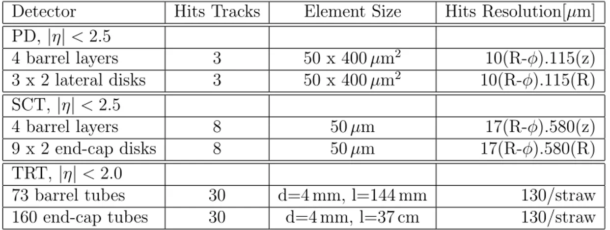
The Inner Detector is a 6.2 m long apparatus with a diameter of 2.1 m, placed around the beam line, with a coverage of |η| < 2.5. Built for the first tracking stage of ATLAS, it is composed of the Pixel Detector, the Semiconductor Tracking and the Transition Radiation Tracker, which technologies and components must be the most radiation hard possible. These are placed in the barrel region and in the end-cap region of ID. The Figure 1.6 shows their configuration, dimension and coverage, while in the Table 1.1 important characteristics are described.
Figure 1.5: Scheme of the ATLAS layout.
Detector Hits Tracks Element Size Hits Resolution[µm] PD, |η| < 2.5 4 barrel layers 3 50 x 400 µm2 10(R-φ).115(z) 3 x 2 lateral disks 3 50 x 400 µm2 10(R-φ).115(R) SCT, |η| < 2.5 4 barrel layers 8 50 µm 17(R-φ).580(z) 9 x 2 end-cap disks 8 50 µm 17(R-φ).580(R) TRT, |η| < 2.0
73 barrel tubes 30 d=4 mm, l=144 mm 130/straw
160 end-cap tubes 30 d=4 mm, l=37 cm 130/straw
Table 1.1: Characteristics of the detectors of ID.
the p-p interaction. It is a Silicon based detector which uses the pixel technologies; it has the highest granularity in all ATLAS and it consists of 4 barrels (Insertable B-Layer, B-Layer, Layer1, Layer 2) and 3 disks for each side. It will be described in more details, especially in its off-detector read-out part, in the next chapter; • The SemiConductor Tracker (SCT) is 4 layers a Silicon microstrip detector.Each
layer is formed by modules composed by two microstrip detector bounded together and glued with a 40 mrad angle of their planes, layout used to obtain a better z-measurement. The two microstrip detectors of a single module are glued with the angle between the two microstrips shifted of 90◦. In the barrel region the plane of the microstrip detector is parallel to the beam line, while in the end-cap region is perpendicular;
• The Transition Radiation Detector (TRD) is the largest track detector of ID and surrounds the other 2. It consists of a large number, about 5 × 10⁴, of straw tubes, that are cylindrical tubes with one positive wire in their inside and the internal wall at negative voltage. The straws all together contribute to the measurement of the particle momentum thanks to the high number of hits, and each one is filled with a mixture of Xenon (70 %), CO2(27 %), and O2 (3 %). In the barrel region the
tubes are parallel to the beam line, while in the end-cap region are perpendicular. There are two algorithms used to reconstruct the particle track:
• the inside-out algorithm, in which primary tracks of charged particles born from primary reactions are reconstructed using 3 seeds in the Silicon detectors (SCT and PD) and then the successive hits are added by a combinatorial Kalman-fitter algorithm;
• the outside-in algorithm, where the hits in TRT of secondary charged particles, formed by decays from primary particles or other secondary particles, are used to reconstruct the tracks adding the Silicon hits always with the combinatorial Kalman-fitter algorithm, if there are. Efficiency of track reconstruction is measured by simulated events, and it varies as a function of pT and η.
1.6.2
Calorimeter
The ATLAS calorimeter system is composed by sampling calorimeters, with the absorber made of Lead, Copper or Iron and the active medium composed by plastic scintillator and liquid Argon. The inner calorimeter is the electromagnetic one, after which there is the hadronic calorimeter. Each calorimeter consists of 4 parts: a barrel part, an extended barrel part, an end-cap part and a forward part. This system includes a pseudorapidity up to |η|=4.9 and a complete φ coverage. The resolution of a sampling calorimeter can be written as σ(E) E = a √ E ⊕ b E ⊕ c where:
• the first term is called the stochastic term and comes from intrinsic fluctuations of the secondary particles of the shower due to their statistical behavior;
• the second term is due to the electronic noise of the read-out channel;
• the third term is a constant that considers temperature, age of detector, radiation damage, and other factors.
The energy resolutions are different based on the calorimeter: σ(E)E = 10%E + (1.2 ± 0.1+0.5−0.6)% for the electromagnetic calorimeter in the barrel region, from 0.13 to 0.06
for the hadronic one in the barrel and end-cap region when pT increase, σ(E)E = 100%E +
(2.5±0.4+1.0−1.5)% for the forward electromagnetic calorimeter. A scheme of the calorimeter
system is shown in Figure 1.7 .
1.6.3
Muon Spectrometer
High pT muons provide signatures for many physics processes studied in ATLAS. This
makes the Muon Spectrometer very important. It is designed for high precision and resolution in the measurement of high pT muons and it also provides an independent
muon trigger. It is divided in barrel and end-cap region. It has barrel and end-cap toroid magnets, and it’s composed by 4 different detector technologies, divided in 4 detectors which can be divided in 2 precision tracking detectors and in 2 trigger chambers. We have the Monitored Drift Tube (MDT) chambers which provides the measurement of
Figure 1.7: Scheme of the calorimeter system of ATLAS
momentum and track in the barrel and end-cap regions, the Cathode Strip Chambers that have the same purpose of MDT but are positioned close to the beam pipe in the innermost layer of the end-cap. Then there are 2 trigger detectors: the Resistive Plate Chambers in the barrel region and the Thin Gap Chambers in the end-cap region. This whole system recognizes muons for which |η| < 2.7, with a threshold of pT > 3 GeV,
since muons with lower energy lose it completely before the Muon Spectrometer, and with a resolution of pT measurement of about 20 % at 1 TeV. The muons energy limit
for momentum measurement is 3 TeV. In Figure 1.8 is shown the scheme of the Muon Spectrometer.
1.6.4
Magnetic System
ATLAS use a system of superconducting magnets (shown in Figure 1.9 ) for the measure-ment of the charged particles momeasure-mentum. The system is composed by a Central Solenoid (CS) surrounding the Inner Detector, and by a system of 3 large air-core toroids (1 barrel and 2 end-cap) generating the magnet field of the Muon Spectrometer, with a dimension of 26 m in length and 20 m in diameter. The CS, for the momentum measurement of ID, has a magnetic field of 2 T and it points in the positive z-axis direction, while the toroids magnet emits a magnetic field of 3.9 T (barrel) and 4.1 T (end-cap). The entire system work at 4.7 K of temperature. The most important parameters for momentum
Figure 1.8: Scheme of the Muon Spectrometer of ATLAS
measurements are the field integrals over the track length inside the tracking volume: I1 = 0.3 pT Z l 0 B sin(θ) (d−→l ,−→B)dl and I2 = 0.3 pT Z l sin(θ) 0 Z r/ sin(θ) 0 B sin(θ) (d−→l ,−→B)dldr
where I1 is the measurement of bending power field (pT=q x bending power=q x (B x
L)) and I2 represents the total transverse deflection of the particle from its initial path. θ represents the longitudinal component of the angle between the track and the magnet field and the integrals are calculated on the azimuthal direction of the particle (l=r/sen θ) and on the radial trajectory of it.
1.7
ATLAS Trigger
Thanks to the high luminosity (L=1034 cm−2s−1), LHC produces in 1 second an order of
magnitude of 108 proton-proton processes, but the electronics for the read-out can reach
only a recording speed of 300 Hz. For this reason ATLAS has a system of multi-level trigger composed by a series of 3 triggers: Level-1, Level-2 and Event-Filter trigger. In Figure 1.10 a scheme of the TDAQ of ATLAS is shown. Level-1 trigger is a hardware
Figure 1.10: Scheme of the Trigger and Data Acquisition of ATLAS
based trigger that divides the data read by high pT leptons, photons, jets and large
missing and total transverse energy. It reduced the rate of data down to 50 kHz approx-imately with a decision time for each collision of 2 µs from the collision (where 1 µs is
the time due to cables). The data for this trigger arrives from the calorimeters and from the Muon Spectrometer, in particular from the RPC and the TGC chambers. Level-1 trigger defines the regions in η and φ coordinates where the other subsequent triggers will start their work, regions called Regions of Interest (ROI); furthermore Lv1 muon trigger searches for coincidences of hits in different trigger stations within a road pointing to the interaction point, because the width of this road is correlated with the transverse momentum. There are 6 muon pT thresholds governed by the hardware-programmable
coincidence logic for this trigger, 3 for the range 6-9 GeV (low pT) and 3 for the range
9-35 GeV (high pT). Level-2 trigger is a software based trigger which starts from ROIs
defined in Lv1 and uses all the detector informations in these regions in its trigger algo-rithms. It permits to reach less then 5 kHz in less then 50 ms. Event Filter is the final stage of the trigger chain and it reaches the rate of approximately 300 Hz in less then 4 s. This time isn’t due by algorithms, instead it’s the time of the standard off-line event reconstruction of ATLAS. There is a trigger menus, where there’s a list of characteristics of an event like Et miss, etc., with a certain threshold (given by the luminosity) for each
one. Those events that passed the selection criteria of this menus are tagged and sorted into data streams. In addiction with these data streams there are also the streams due to the calibration data of the detector. Lv2 with Event Filter trigger formed High Level Trigger.
Chapter 2
Pixel Detector
Now we will talk more in depth of the Pixel Detector. Its layout is based on 4 layers with a high radiation hardness electronic and high resolution, and it has the important task of tracking the first particles produced by the proton-proton collisions, and measuring the interaction vertexes. The layers are, from the closest to the farthest from the beam pipe: Insertable B-Layer, B-Layer, Layer-1, Layer-2, with a total of 112 staves, each one formed by 13 modules; these modules are tilted respect the z-axis of 1.1◦, while the staves are tilted of 20◦ on the x-y plane. In Figure 2.1 and 2.2 are shown the positioning
Figure 2.1: Image of the layout of the Pixel Detector staves
of the staves and the modules respect the coordinate system, while in Table 2.1 are
Layer Mean Number of Number of Number of Active
Radius (mm) Staves Modules Channels Area (m2)
B 50.5 22 286 13178880 0.28
L-1 88.5 38 494 22763520 0.49
L-2 122.5 52 676 31150080 0.67
Total 112 1456 67092480 1.45
Table 2.1: Characteristics of the Pixel detector.
written some characteristics of the Pixel Detector’s inner detectors. Here and in the next section we will talk about the 3 layers more outside. About IBL, because of its different technology, we will talk later.
2.1
Modules
The modules that composed the staves are formed by: 16 Front end (FE-I3) sensors chips which are responsible for reading signal from the sensors, a flex-hybrid, a Module Controller Chip (MCC) and a pigtail. In Figure 2.3 a scheme of a module is shown,while in Figure 2.4 is shown a scheme of the connection between the pixel sensors and the read-out chips (FE-I3). An FE-I3 is 195 µm thick and 1.09 by 0.74 cm2 large and counts
3.5 x 10⁶ transistors in 250 nm CMOS technology. Each one is bump bounded over the sensors and each analog amplifier can discriminate signals of 5000 electrons with a noise threshold of 200 electrons. These signals are then digitalized and buffered inside the End Of Columns (EOC) electronic waiting for the trigger signal. EOC signals are sent to MCC which distributes timing, trigger, reset and calibration signals. The signals of 6 MCCs are converted from electric to optic by the opto-board to the Back Of Crate board, where the opto-board has:
• PIN diode, that converts the signals from optic to electric;
• Digital Optical Receiver Integrated Circuit (DORIC), which adapts the electric signal from LVDS Standard to PIN signals;
• Vertical Cavity Surface Emitting Laser (VCSEL), that converts electrical to optical; • Virtual Device Context (VDC), that interfaces MCC and VCSEL.
Each module is made of a 256 µm thick crystalline Silicon layer and contains 47232 pixels, where 41984 are 400 by 50 µm and the other are 600 by 50 µm, which are located in the external side to minimize signal loss in the region between the modules.
Figure 2.3: Image of the layout of the Pixel Detector modules.
2.2
Sensor
As we said, the Pixel Detector is a semiconductor detector based on Silicon, where a n-doped crystalline semiconductor with p-doped well forms a pixel of the detector. This connection (similar to a diode) is reverse polarized, so the deplection region extends until a ionizing particle pass through the pixel and frees electrons and holes. These drift, for the electric field, toward the metal contacts, which have attracted them, and then they collect these charges. The energy released by the charges is proportional to the collected charges, and, obviously, by the pixel giving a signal, and by the signal itself we can obtain the particle track. The effects of the radiations on the pixels are:
• increment of leakage current, which forces to use a better cooling system;
• the change from n-type to p-type of the substrate, and the consequent shift of the p-n junction to the lower part of the pixel; this problem can be solved enhancing the bias voltage gradually from 150 V to 600 V, fact that decreases the life of the pixel.
To reduce the damages from the radiation it can adding Oxygen atoms to the crystalline structure, keep the Silicon at -20◦ C because the increase of temperature in the substrate during the data taking is caused by the increase of dopant absorbed by it, creating p-doped dividing zones in the n-p-doped wells. A scheme of the sensor is shown in Figure 2.5 .
2.3
IBL
IBL is the first detector of the ATLAS chain and the last that was joined to the Pixel Detector. The motivations are situated in the b-tagging capability decrease of B-Layer due to the luminosity increase of LHC and to the consequent enhance of radiations, and so of damages, in the detector B-Layer, and obviously in the research of a better tracking precision. The IBL technology is different because of the more radiation power and the more surface covered (where this task is performed thanks to the new chip FE-I4).
2.3.1
IBL Sensor and Modules
Sensors and modules of IBL, as we said, use different technologies respect the other layers. There was 2 candidates, shown in Figure 2.6 and 2.7 :
Figure 2.6: Image of planar sensor in thin border configuration.
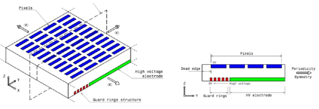
• the Planar Sensors has the layout of a ”normal” Silicon sensor. They were used in B-Layer too but in IBL they are slightly different, in fact the inactive border has to pass from 1 mm to 450 µm and the NIEL has to double from the old value of 2 x 10¹⁵neq/cm2 to make acceptable the effects on the signal. Furthermore,
from studies made for B-Layer, we now know that a sensor under radiation can double the collected charges if reduces its thickness, because reducing the thickness, consecutively the probability to lost particle’s track because of trapping, induced by the radiation damage, reduces too. They request 1000 V for the bias voltage. There are 3 possible configurations: conservative, thin border, thin p-doped substrate. • 3-D sensors have a completely different geometry from the planar ones; they read
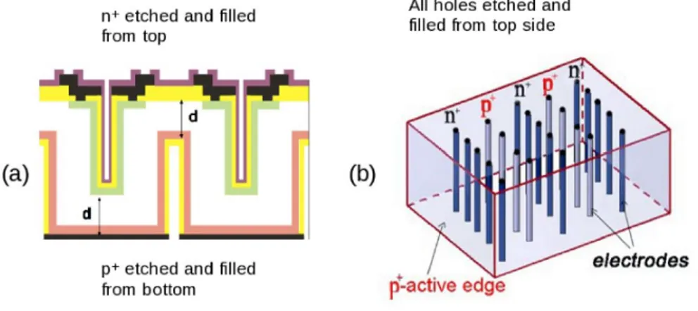
the signal from the charges collected from 2 electrodes at once due to the low number of charges, and for this double reading the noise increases. The etching
Figure 2.7: Scheme of 3-D sensor, in double sided (a) and full-3D (b) configuration.
during the productive process is the difference between full 3-D sensor and double-sided ones. Furthermore the active area of the full 3-D extends much more to the surface reducing the not sensible volume, and these sensors are more closer each other in the plane, reducing the voltage bias (150 V) and so the leakage current. Efficiency decreases of 3.3 % if a particle passes near the electrode, but this only in the case the sensor is in perpendicular position to the particle, that isn’t our case because the sensors are tilted of 20◦.
2.3.2
FE-I4
The LHC luminosity and the small distance of IBL from the beam pipe has been driven to upgrade the chip for the detection of the particles from FE-I3, that isn’t good enough to maintain the request efficiency, to FE-I4. This chip, designed for IBL detector, is built with a 130 nm CMOS technology, a thinning down of the gate oxide for an enhance in the radiation tolerance, and in a 8 metal option with 2 thick Aluminium top layers for better power routing. Furthermore, the current drain architecture of FE-I3 scales badly with high hit rates and increased front-end area; for these reasons the FE-I4 pixel dimensions are 50 x 250 µm2, with an increase of z-axis track resolution and a reduction of the pixel
cross-section. The active area of FE-I4 is close to 90 %, given by the active size of 20 mm (z-direction) by 16.8 mm (φ-direction) and with 2 mm more foreseen for the periphery, layout containing an array of 80 by 336 pixels each one with an analog and a digital component. The biggest size of FE-I4 takes to important benefits like the reduction of material for the detector layer and the enhance of the physics performance like the b-tagging efficiency vs. the light quark rejection factor, and furthermore obviously the
reduction of costs. The layout of the FE-I4 is shown in Figure 2.8 .
Figure 2.8: Scheme of FE-I4 read-out chip.
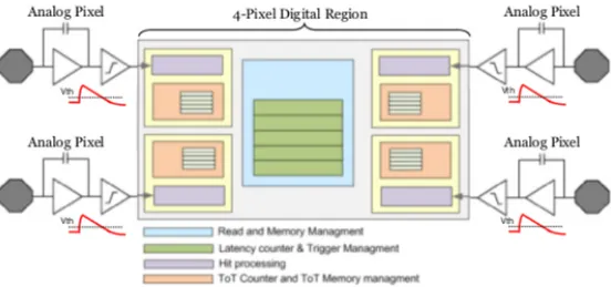
Digital Section
The FE-I4 uses a different method for the storage of pixel hits, completely different from the column drain architecture. It uses a local storage of the pixel hits in buffer located at pixel level, in a region of 2 by 2 pixels, where the 4 pixels are tied together at digital logic point of view and they shared the same digital processing (see Figure 2.9 ). This architecture takes advantage from the small feature size of the 130 nm CMOS technology, reducing the loss in hits recording below to 0.6 % at luminosity 3 times more then the actual, saving area and reducing power. Furthermore now the recording of small number of electrons, where this recording is most of the time located near a large signal recording by the pixels, happens without being time-stamped, giving an handle
Figure 2.9: Scheme of FE-I4 Double Column system.
on time-walk. A Double-Column contains the 4 pixel region and its logic, with a clock of 40 MHz (the bunch-crossing of LHC). Here 4 adjacent pixels share latency counter, trigger, read and memory management units. The 8-bit latency counter counts down a programmable latency. The individual components are the Time Over Threshold 4-bit counters and the hits processing circuitry. A start due to a particular event, coming from any discriminator, starts the latency counter, which is only one even for several signals from several pixels in the same bunch-crossing. The time which the pixel comparators stay above threshold tells us the dimension of the hits. The read-out is based on a dual token between Double-Column and End of Column which make triple redundant with majority voting to yield enhancement. A pixel configuration shift register runs in each Double Column to tune each pixel singly, and redundant always to yield enhancement. The End of Column logic is kept very simple and serves only as a dedicated interface between each one of the 40 Double Column and the digital control block with its FIFO. Analog Section
The analog section of the chip, shown in Figure 2.10 , which cover 50 by 150 µm2 of the size of FE-I4, is implemented as a 2-stage architecture, optimized for low power, low noise and fast rise time, followed by a discriminator. The first stage is an adjusted cascode pre-amplifier with a triple-well NMOS input, containing an active slow differential pair, tying the pre-amplifier input to its output, and used to compensate sensor radiation-related leakage current. The section has a 100 nA DC leakage current tolerance. The second stage is AC coupled to the pre-amplifier and implemented as a PMOS input
Figure 2.10: Scheme of FE-I4 Double Column system.
folded cascode; this coupling comports two benefits: the decouple of the second stage by the leakage current related to DC potential shift and gives an additional gain factor, coupling capacitance to feedback capacitance, always in the second stage, of 6. This permits to increase the feedback capacitance of the first stage without degrading the signal amplitude at the discriminator input, and giving benefits like the enhance of charges collection efficiency, signal rise time and power consume.
Chip Periphery
The FE-I4 periphery has the sequent tasks: communication and operational configu-ration of the integrated circuit (IC), organization of the data read back and fast data output serialization. New blocks are implemented for future prototype functions and to provide extra testing capabilities like redundant memories, low-speed multipurpose multiplexer. Two LVDS inputs are required to communicate with the FE-I4: the clock at 40 MHz and command input Data-In (40 Mb/s). The command decoder of FE-I4 is based on the architecture for the module control chip. Its stream is decoded into local pixel configuration and global configuration, trigger commands. The local registers for pixel configuration are 13 bits deep, while for global configuration the 32 registers are 16 bits deep. In the bias generator section, based on an internal current reference, DACs convert the stored configuration values to voltages and currents needed to tune all the IC sections. The decoded trigger is sent to the pixels and to the End of Chip Logic block where the readout is initiated. The data stored in the 4-PDR ToT buffers are sent to the periphery only when a trigger signal that confirms an hit is sent, then data
are associated to the specific bunch-crossing corresponding to the specific trigger. The trigger confirms an hit when the coincidence of a trigger with latency counter reaches its latency value in 4-PDR. At this point the 4-PDR address and the 4 ToTs are propagated to the End of Chip Logic, where the transmitted signals are Hamming coded to yield enhancement. Then the data are re-formatted and stored in a FIFO to be sent out. The re-formatting is due to band-width reduction and facilitate the following data processing steps. Further the data, the pixels send even information describing its status for the diagnostic from the global registers. The data are then encoded in an 8b/10b custom protocol, in Data Output Block, and serialized at 160 Mb/s, a fast serialization made possible by the use of a speed clock formed by a Phase Locked Loop clock generator.
2.4
BOC-ROD System
After the detection of the particles by the semiconductor detector and the acquisition of the relative signals from the on-detector read-out (the read-out system which is located in the area subjected to radiation damages), these signals are sent to the off-detector part of the readout system of IBL, shown in Figure 2.11 . This infrastructure is composed by:
Figure 2.11: Scheme of BOC-ROD system.
• Back of Crate (BOC) board; • ReadOut Driver (ROD) board; • VME Crate;
• Single Board Computer (SBC);
• S-Link to send data from the BOC to the ATLAS TDAQ system; • optical module to connect the BOC with the Front-End chip (FE-I4);
• Ethernet connections at speed of 1.12 Gb/s to send histograms for calibration anal-ysis and configuration data for FE-I4.
Starting from the received data from 32 FE-I4 (bandwidth of 5.12 Gb/s), these data are sent to the BOC by optical modules, which consequently send it to the ROD encoded with an 8b/10b code, where these data are processed. After that the data are sent to two different ways: to the BOC again and then by 4 S-Link to ATLAS TDAQ system (5.12 Gb/s connection), and to the PC farm for the calibration histograms. Furthermore, thanks to a GB Ethernet connection, it’s possible to send data from the BOC to 16 FE-I4 to configure them, where originally the configuration data were produced in the ROD and then sent to the BOC. Each one of these off-detector systems can interface 32 FE-I4 in input and 16 in output.
2.5
BOC-ROD Comunication
The BOC-ROD interface carries all data which has been received from the detector. There are 96 lines with SSTL3 (Sub Series Terminated Logic) I/O standard between the cards. The 96 lines are divided into 8 12-bits wide data busses. Each data bus transfers the data of 4 front end chips at a rate of 80 MHz. Data lines carry the decoded 8b/10b data of the channels and the control lines show if the data is a 8b/10b-k-word.
2.6
IBL-BOC
The IBL-BOC functions are to receive data from the front end, to send configuration data to it and provide the clock for the on-detector part. This clock is generated in the TIM board and it’s sent to the BOC where it can be delayed, subsequently the PLL generates copies of this clock to send them where is necessary. The management of the clock is handled by the BOC FPGAs, which are 1 BOC Control FPGA (BCF) and 2 BOC Main FPGAs (BMF). A photo of the IBL-BOC is shown in Figure 2.12
2.6.1
BCF
BCF (a Spartan 6 FPGA) provides at the control of BOC. The central component of the firmware is a Wishbone interconnect which gives to all the peripheral the basis of the configuration for the access. To this interconnect are connected a Setup-Bus connector
Figure 2.12: IBL-BOC.
and a Microblaze processor. The latter configures the ethernet access to the BOC and provides some control tests for the board. Setup-Bus (shown in Figure 2.13 ) is an asynchronous configuration interface between BOC and ROD with 16 addresses, 8 data and 3 control lines. The FPGA’s configuration follows the sequent steps: BCF loads its configuration from a 64 Mbit SPI Flash in Master Serial Peripheral Interface mode; then BCF reads the configuration settings of BMFs from another SPI Flash and downloads it via the Slave Serial configuration ports; in the end BCF loads the software, which depends to the last configuration, from a third SPI Flash.
2.6.2
BMFs
BMFs (2 Spartan 6 FPGAs) encode the configuration data from ROD into a 40 Mb/s serial stream and then send it to the front-end. The TX path is used to send commands and trigger to the modules. In normal detector operation it is used to do the Bi-Phase Mark (BPM) encoding (shown in Figure 2.14 ) of the incoming data from ROD, to adjust the detector timing using coarse and to delay blocks. The coarse delay has implemented a variable-tap shift register clocked at 160 MHz. The RX path in the firmware is responsible for the reception and decoding of the incoming detector data, after that the decoded data are collected and multiplexed to ROD.
Figure 2.13: Scheme of the Setup Bus.
2.7
IBL-ROD
The second board, which manages the off-detector readout, is the IBL-ROD, that is the upgrade of the ATLAS Silicon Read Out Driver (SROD), used in the SCT and Pixel B-Layer, L1 and L2. Project and firmware of the ROD are mainly developed in Bologna, and it provides the data gathering and subsequently building of the event fragments, and the calibration histograms building. ROD has: 1 Digital Signal Processor (MDSP, currently not used), 1 Program Reset Manager (PRM) FPGA, 1 ROD Controller FPGA, 2 FPGAs slave, 1 Phase-Locked Loop (PLL), 32 MByte SDRAM DDR, 4 Mbit and 64 Mbit FLASH memories, 2 GByte DDR2 SODIMM, 3 Gbit Ethernet connections. A photo of the IBL-ROD is shown in Figure 2.15 .
Figure 2.15: IBL-ROD.
2.7.1
ROD Controller
The control FPGA in the ROD is made by a Virtex 5 which has the role of Master of the Read Out Driver, FPGA which manages with: the FE-I4s, the triggers that comes from the TTC Module and all the information that refer to the trigger itself. Embedded in the FPGA there’s a Power PC (PPC) microprocessor. The Master blocks are:
• Event ID and Trigger Processor, which process the event data and then sends them to the FPGAs Slave, and tells to the FE Command Processor to generate and send the configuration data to the FE. It can be driven by the PPC or by the TIM; • FE Command Processor, which generates and sends commands to the FE if
re-quired, and generates Lv1 trigger if TIM issues a trigger;
• Event Processor, where Event ID, Trigger Type and Bunch Crossing ID are sent to the Event Fragment Builder of the Spartan Slaves.
A logic block of the Master is shown in Figure 2.16 .
Figure 2.16: Scheme of the ROD Master firmware block.
2.7.2
Spartan Slave
The slave FPGAs are Spartan 6 with a Microblaze processor emulated on them. These FPGAs: process the data took from the FE-I4, collect histograms to a SSRAM and send them to an histogram server, if needed, through a Gb Ethernet connection programmed always by the Spartan 6. The firmware logic blocks of the Slaves are shown in Figure 2.17 and are:
• Dual Clock FIFO, which connect the 80 MHz clock of the bus and the 40 MHz clock of the FPGA;
• Event Fragment Builder, where the data coming from the front end are added with header and trailer infos as trigger type, event ID or bunch crossing ID;
• Inmem FIFO (accessible by the PPC), which has the task to debug by collects all inputs from the BOC-ROD buses and verified the data, even before entering the gatherer zone, and giving a perspective of what should happen;
• Histogrammer, where the histograms are collected, histograms which contain in-formation about calibration runs.
2.7.3
PRM
The PRM (a Spartan 6 FPGA) interfaces with the VME bus, the ROD Controller FPGA, the slave FPGAs and the PLL. It has the important role of programming and resetting the ROD FPGAs.
2.7.4
SBC
Single Board Computer is a computer mounted on a 6U board which: programs some ROD components, controls all the operations of the VME on the ROD and monitors the ROD’s components temperature.
2.7.5
Lattice PLL
Lattice ispClock 5620 Phase-Locked Loop (PLL) is a control system which generates clocks based on clock connected in input to it, comparing the phase and frequency of the clocks in input and output and varying them until the clocks match. It is composed by the following blocks:
• Phase Detector (PD), which generates the voltage representing the difference in phase between the clocks, and sends this voltage to the Voltage-Controlled Oscil-lator (VCO) which maintains the difference constant;
• Loop Filter, which has two functions: decides how the loop must behave in case of disturb, limits the reference frequency energy output by the PD so that it can reduce the spurs that can be produced;
2.7.6
S-Link
A Simple LINK (S-Link) is a link that can be thought of as a virtual ribbon cable, moving data or control words from one point to another. It is shown in Figure 2.18 .
Figure 2.18: Scheme of the S-Link.
The specification describes the interface between the Front-end Motherboard (FEMB) and the Link Source Card (LSC), and the interface between the Link Destination Card (LDC) and the Read-out Motherboard (ROMB). It does not describe the physical link itself. Further the simple data moving, S-Link includes:
• Control/Data bit, where all the words transmitted are accompanied by an addi-tional bit which enables the user to mark any word and thus identify it;
• Error Reporting, using an LDERR line, a S-link detects transmission errors and reports them. Furthermore data error LED is illuminated and held until reset; • Test Function, where LSC and LDC are transformed in a transmitter and a receiver
of fixed pattern which are verified by LDC, mode called test mode. If data error are revealed, the data error LED is illuminated by LDC; furthermore LDC can transfers test pattern to the ROMB;
• Reset Function, which provides an hard reset for LSC and LDC.
2.7.7
TIM
The Trigger Timing Controller Interface Module interfaces the ATLAS Lv1 trigger with the Read-Out Drivers of the Pixel Detector using the LC-standard TTC and Busy sys-tem. It makes the following tasks:
• propagates the clock of TTC all over the experiment; • receives and upgrades the triggers;
• keeps updated the TTC with Bunch and Event Counters via Bunch Counter Reset and Event Counter Reset;
TIM has 2 FPGAs where one has generic functions for the TIM (VME Interface, local bus control, board reset, sending of status information to the second FPGA), while the other provides interface with the FE panel and ROD backplane signals. A photo of the TTC board is shown in Figure 2.19 .
Chapter 3
Pixel-ROD
The read out system just described did and is doing diligently its work of reading data from the front end, and sending them to the ATLAS TDAQ and PC farm. It was built and configured for the current LHC luminosity of 1034 cm−2s−1 and the current bunch crossing frequency of 40 MHz. It permitted, with all the ATLAS experiment, to reach many important achievements, but now the game rules will change. The future LHC upgrade (after LS2 and LS3) will enhances these numbers significantly, as the Table 3.1 show. In this future situation the BOC-ROD read out system will must be upgraded to
Figure 3.1: Future LHC features, with High Luminosity LHC numbers.
provide the efficiency need for the future CERN physics. There are some projects for new read out system working and concurring for the tasks required by the future physics at CERN. The most important technology that the next read out system will must develop are the PCIe connections (because this is the direction in which the read out projects of ATLAS and even CMS are going), the transceiver connections, the capacity to process and transport a bigger amount of data respect at which it was never be produced. Searching for these characteristics, the boards choose to achieve the new physics goal are the KC705 and the ZC702, 2 Xilinx evaluation boards. The project idea of the INFN
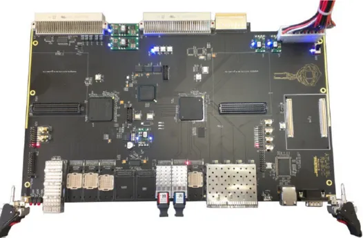
laboratory and of the Department of Physics and Astronomy laboratory of the Bologna University was to use the knowledge from the experience achieved with the IBL-ROD and use it in a new board born from the fusion of 2 boards with different characteristics, that united in 1 will substitute the BOC and the ROD and will increase the performance. The name choose for this board is Pixel-ROD (PR), showed in Figure 3.2 .
Figure 3.2: The Pixel-ROD board.
• KC705 is an evaluation board of the Xilinx with a programmable FPGA and with a high connection capability even with high speed (up to 12.5 Gb/s). Recalling what said in the previous section, the KC705 has a PCIe Gen2 8x connector with a nominal transmission speed of 4 GB/s (2.5 GB/s during the tests), which permits to connect the board directly to a pc (of the ATLAS TDAQ or of the pc farm) and to leave the old VME bus with its 160 MB/s of speed. The high speed connections are the 16, opto-electrical or electrical, input and output connectors which can reach a transmission speed of 12.5 Gb/s each one. In the end the Kintex-7 FPGA is a powerful instrument which can be used to upgrade the slave work of the readout system.
• ZC702 is, like the KC705, a Xilinx board which is the choose Master for this readout system project. Its most important feature is the ARM-Cortex A9 MPCore processor embedded in the Zynq-7000 FPGA which surpasses in brutal strength the PowerPC 440 processor embedded in the Virtex 5 FPGA, indeed we have 667 MHz frequency for PPC against 1 GHz of the ARM, 256 kB level 2 cache against 512 kB, same level 1 cache (32 kB), etc.
3.1
Pixel-ROD
In this section we will talk about the Pixel-ROD specifications, Pixel-ROD defined as a read out PCIe based board with Master-Slave system.
3.1.1
FPGAs
The PR is provided with 2 FPGAs, a Zynq-7000 XC7Z020-1CLG484C and a Kintex-7 XC7K325T-2FFG900C, which now will be described the major features.
Kintex-7
The FPGA Kintex-7 represents the multi-high speed connection controller with the out-side of the board. XC7K325T-2FFG900C has the following characteristics:
• advanced high-performance FPGA logic based on real 6-input logic Look-up table (LUT) technology configurable as distributed memory;
• high performance SelectIO technology with support for DDR3 interface up to 1866 Mb/s;
• high speed serial connectivity with build-in multi gigabit transceivers from 600 Mb/s to maximum 12.5 Gb/s;
• a user configurable analog interface (XADC), incorporating dual 12-bit 1MSPS analog-to-digital converters with on-chip thermal and supply sensors;
• DSP slices with 25 x 18 multiplier, 48-bits accumulator, and pre-adder for high-performance filtering, including optimized symmetric coefficient filtering;
• powerful Clock Management Tiles (CMT), combining Phase-Locked Loop (PLL) and Mixed-Mode Clock Manager (MMCM) blocks for high precision and low jitter; • integrated block for PCI Express (PCIe), x8 Gen2 Endpoint and Root PortR
designs;
Zynq-7000
The FPGA Zynq-7000 represents the general controller of the PR, the Master of the Kintex-7 to which the configuration board commands move from the users, and from them move toward the Slave. The XC7Z020-1CLG484C features for the Programmable Logic (PL) part are the following:
• 6-input logic Look-Up Table (LUT) technology configurable as distributed memory; • DSP slices with 25 x 18 multiplier, 48-bits accumulator, and pre-adder for high-performance filtering, including optimized symmetric coefficient filtering, optional pipelining, optional ALU;
• 4.9 Mb Block RAM (140 36 kB blocks);
• a user configurable analog interface (XADC), incorporating dual 12-bits 1MSPS analog-to-digital converters with on-chip thermal and supply sensors.
The major characteristic provides by XC7Z020-1CLG484C is the embedded ARM Cortex A-9 MPCore processor. It’s the Processor System (PS) part of the Zynq-7000, and toward are described the most important components.
Application Processor Unit (APU)
The APU contains 2 processors which share, with a NEON co-processor, a 512 kB Lv 2 cache (for instruction and data), while each processor implements a 32 kB Lv 1 cache. The architecture is the ARM v7-A, which supports ARM, Thumb (for which the single instruction multiple data (SIMD) instructions are available) and Java instructions, with full virtual memory support and with the instructions added by the NEON co-processor. The configuration is a MP with a Snoop Control Unit (SCU) which maintains coherency between Lv 1 and Lv 2 caches and manages the Accelerator Coherency Port (ACP) interface from the PL. In parallel with the Lv 2 cache there’s a 256 kB On-chip Memory Module (OCM) that provides a low-latency memory. ACP facilitates communication between PL and APU. All accesses through the Lv 2 cache controller can be routed to the DDR controller or can be sent to other slaves in the PS or PL depending on their address. To reduce latency to the DDR memory, there is a dedicated port from the Lv 2 cache controller to the DDR controller. The architecture supports TrustZone Technology to help to create a secure environment to run applications and protect their contents. The Memory Management Unit (MMU) works to memory protection, controlling access to and from external memory and translation virtual memory (addresses) to physical addresses.
Interconnect
The interconnect located within the PS comprises multiple switches to connect system re-sources using AXI point-to-point channels to communicate addresses, data, and response transactions between master and slave clients. This ARM AMBA 3.0 interconnect im-plements a full array of the interconnect communications capabilities and overlays for Quality of Services (QoS), debug and test monitoring. QoS resolves contention in the central, master, slave and memory interconnect.
DDR Memory Controller
The DDR memory controller supports DDR2, DDR3, DDR3L and LPDDR2 devices, and consists of three major blocks: an AXI memory port interface (DDRI), a core controller with transaction scheduler (DDRC) and a controller with digital PHY (DDRP). The DDRI block interfaces with 4 64 bits synchronous AXI interfaces to serve multiple AXI masters simultaneously. Each AXI interface has its own dedicated transaction FIFO. The DDRC contains two 32-entry content addressable memories (CAMs) to perform DDR data service scheduling to maximize DDR memory efficiency. It also contains fly-by channel for low latency channel to allow access to DDR memory without going through the CAM.
I/O Peripheral
The PS I/O peripherals, including the static/flash memory interface, share a multiplexed I/O (MIO) of up to 54 MIO pins. Zynq-7000 AP SoC devices also include the capability to use the I/Os which are part of the PL domain for many of the PS I/O peripherals. This is done through an extended multiplexed I/O interface (EMIO). Software programs the routing of the I/O signals to the MIO pins. The I/O peripheral signals can also be routed to the PL (including PL device pins) through the EMIO interface. This is useful to gain access to more device pins (PL pins) and to allow an I/O peripheral controller to interface to user logic in the PL. The I/O multiplexing of the I/O controller signals differ; indeed, some IOP signals are solely available on the MIO pin interface, some signals are available via MIO or EMIO, and some of the interface signals are only accessible via EMIO.
3.1.2
Memory
The physical memory installed on the Pixel-ROD are: • 2 GB DDR3 RAM SODIMM (Kintex-7);
• 2 128 Mb Quad SPI flash (1 for Kintex-7 and 1 for Zynq-7000); • 1 128 MB parallel flash memory (Kintex-7).
3.1.3
Internal Bus
The Pixel-ROD has 3 types of internal buses that connect directly the 2 FPGAs: • a 21 bit differential bus;
• a 5 bit single line bus;
• a 1 bit differential bus dedicated to share the differential internal clock of the board between the FPGAs.
3.1.4
I/O
Some input and output from the original schematic of KC705 and the ZC702 have been removed for a more useful purpose. These removed components are: the HDMI port (KC705 and ZC702), SD card reader (KC705 and ZC702), some GPIOs and LEDs (KC705 and ZC702), 1 of the 2 FMC LPC connector (ZC702), the USB port (ZC702), the PMODS connection (ZC702). The connection from the board and to the board are:
• PCI Express Gen2 x8 (Kintex-7);
• 2 10/100/1000 Ethernet tri-speed (Kintex-7 and Zynq-7000); • 1 FMC HPC VITA 57.1 (Kintex-7);
• 2 FMC LPC VITA 57.1 (Kintex-7 and Zynq-7000); • 2 USB-to-UART (Kintex-7 and Zynq-7000);
• 1 USB JTAG interface (using a Digilent module or header connection); • 2 differential SMA Transceivers (2 in input and 2 in output) (Kintex-7);
• 1 differential SMA dedicated to the transceiver differential clock input (Kintex-7); • 2 SMA for the user (Kintex-7);
• 4 SMA dedicated for the SI5326 component, an Any-Frequency Precision Clock Multiplier;
• 1 SFP+ (Kintex-7);
• a specific connector called PMBUS to connect the 3 UCD9248 chips (see ”Power Supply System”) to a pc.
3.1.5
Components
Other important components of the Pixel-ROD are 2 oscillator that generate fixed clocks (1 for Kintex-7 and 1 for Zynq-7000), and 2 programmable demultiplexer (Kintex-7 and Zynq-7000), which can program:
• clock generators (1 for Kintex-7 and 1 for Zynq-7000);
• a PLL to generate clocks based on clocks in input in it (Kintex); • RAM memory (Kintex-7);
• PMBUS (see later) (Kintex-7 and Zynq-7000).
3.1.6
Switches, Bottoms and LEDs
There are on the board some switches, LEDs and bottoms very important for the con-figuration of the board and for the knowledge of its status:
• 2 bottom to de-program the 2 FPGAs (SW14 for Kintex-7 and SWZ4 for Zynq-7000);
• 2 LEDs from the ”done” signal, which makes enlighten the LEDs when the pro-gramming of a FPGA is gone well (DS20 for the Kintex-7 and DSZ3 for the Zynq-7000);
• a switch (SW20) to configure the board to use the Digilent JTAG chip (01) or the JTAG connector (10);
• a switch (SWZ16) to configure the Zynq-7000 FPGA to use a particular connector or memory to upload the firmware.
3.1.7
Power Supply System
Respect the other structure of the board, the power supply system of the Pixel-ROD has to be re-invented. Indeed, to maintain the possibility to insert the board on a pc case, the power supply systems of KC705 and of ZC702 have been merged and not copied. The 12 V voltage arrives from a Molex connector and it provides power for 3 Digital Pulse-Width Modulation (DPWM) System Controller (UCD9248) chips, which control the power up of the board. This particular power up system is due because the new FPGA technology requires a particular and precise chain of synchronous power up of all the board components. Every UCD9248 is a 4 rail, 8 phases synchronous buck digital PWM controller designed for non-isolated DC/DC power applications. When multiple power stages are configured to drive the voltage rail, UCD9248 distributes
the phases to all the DPWM output in order to minimize the ripple. The UCD9248 integrates dedicated circuitry for DC/DC loop management with RAM, flash memory and a serial interface to support configurability, monitoring and management. In order to facilitate the configuration of these devices, a PC based Graphical User Interface (GUI), named Fusion Digital Power Designer, is provided by Texas Instrument. This tool allows to configure the system operating on parameters for the application, storing the configuration to on-chip non-volatile memory. Furthermore, it is possible to get real time measurements of sensed voltages, once the device is configured and correctly interfaced. The connection from the chip and the pc is made by a dedicated USB adapter and a specific device named PMBUS connector. After the configuration files have been uploaded on the 3 devices, each device can control 4 DC/DC Switching regulators, which are of 3 different types:
• PTD08A020W, a single output switching regulator which supply 20 A; • PTD08A010W, a single output switching regulator which supply 10 A; • PTD08D210W, a double output switching regulator which supply 20 A.
Each UCD9248 manage 4 rails and 4 of the possible phases, and they do it using 4 signals:
• a DPWM output signal through which the switching regulator defines the output voltage;
• a EAN/EAP differential signal which provides the control of the voltage value choose for the output of the switching regulator;
• a Current Sense (CS) input signal which controls the choose range of the output of the switching regulator;
Chapter 4
Preliminary Tests
As the description just exposed shown, the Pixel-Rod is a complex device with important features and incredible versatility. The final task of this device will be to work hours and hours constantly with a continuous stream of data, always active check system and continuous functioning processing system. So, to be sure of the correct functioning of the board, the first step to do to ensure the board capacities is to test its components.
4.1
Power On
The power system of the Pixel-ROD is a complex architecture custom built to allow the union of the KC705 and the ZC702. Because of the complex architecture of the Pixel-ROD, the power on system must not only ”give power” to the board, but it must do it in a particular way to protect the board’s components from damages. To ensure the correct power on, the Pixel-ROD uses 3 chips called UCD9248, power controllers chips which can be programmed by a specific tool designed by the Texas Instrument, the manufacturer of the chips. To reduce the complexity of the test and the danger of damages, the Pixel-ROD power system has been sectioned using solder pads, so that all the parts of the board has been tested separately. After ascertains that all the parts could receive the power, the UCDs were programmed using the software Fusion Digital Power Designer, provided by Texas Instrument, connecting a pc to the board by the PMBUS connector. Because of the Pixel-ROD complexity, the power on it isn’t a normal ”switch and all the board is ready”, but the rail that transmits the voltage in all the board must follow a particular ignition chain. In Figure 4.1 and 4.2 are shown the simulation and a real image, took with the oscilloscope directly by the board, of this chain. The principal problems founded during these tests were: the ”forgot” connection of 2 solder pads, a DC/DC mounted backwards, a couple of feedback signals reversed, a block of 3 signals with the names inverted. This bad lists, tough it may seems a defeat, in fact demonstrates the solidity of the project, because the only problems found have been only
Figure 4.1: Simulation of the ignition chain.
little distraction problems, not great design problems.
4.2
System Clock and Internal Bus Test
Here start my work, indeed my thesis job has been to test some of the Pixel-ROD com-ponents and implements some of the particular firmware for important implementations of this device. As we said, the 2 Pixel-ROD FPGAs are connected directly with 3 type of internal buses. To test these buses, firmware written in VHDL has been used. The idea, for the 5 single line and the differential clock line, was to generate 2 counter with the same frequency in each FPGA, send the data from the Zynq-7000 to the Kintex-7, and start a subtraction operation between the data produced. To synchronise the data to subtract, a signal has been sent from the Zynq to the Kintex. Then, some GPIOs of the Kintex has been used to check the goodness of the transmission, which is shown by a not-asserted signal of the GPIOs on the oscilloscope, made at 200 MHz using as clock the system oscillator. For the 21 bit differential bus, a similar operation has been made, but in this case the subtraction was built subtracting the ”n” data received by the Kintex from the Zynq, and the ”n-1” data. So the result will be always a logic ”1”, apart when the bus will be full of logic ”1” and it will restart the count, or in other word, ”0->21 bit=0” minus ”1->21 bit=1”. In the first case the Kintex will emit a logic ”0” by a GPIO, in the latter case it will emit a logic ”1”. The logic ”1” emission will occur every
tperiod = 221∗
1
200 ∗ 106Hz ' 10.5 ms
. So, using an oscilloscope, it is possible to see the logic ”1” about every 10.5 ms, to be sure of the good success of the test.
4.3
FPGAs RAM Tests
The next test was about the performance of the DDR3 RAM memories installed in the board. For the test was used the Intellectual Property (IP) Integrator, a tool of the Vivado suit, which is a Xilinx software, which permits the production of firmware using cores provided by a catalog available in the Vivado suit, and connecting them with the AXI4 interface. This type of programming method consents to build big and complex structure, like emulating processor, with a relatively simplicity. In this particular case, for the Kintex FPGA, the work has been to implement a Microblaze, a 32 bits soft processor, to allow to ”transform” the Pixel-ROD in a programmable computer where, based on the block needed to test, this block has been instantiated and, as we said with the use of the AXI4 interface, connected to the emulated processor. The most important IP cores used for this test are following described.
Microblaze
This is the core which represents the emulated processor. Completely customizable, the signals with which it works are:
• Clk: represents the reference clock of the design; • Reset: the reset used in all the design;
• Interrupt: this signal manages all the interrupts sent by the other IP cores; • Debug: input always connected with the IP core Microprocessor Debug Module,
which connects the Microblaze to the Xilinx System DeBugger, which permits to send command directly to the soft processor like read or write on its registers; • DLMB and ILMB: Data Local Memory Bus and Instruction. This signals allow
the primary access to the on-chip block RAM;
• M AXI DC and M AXI IC: Master AXI Data Cache and Instruction Cache. This 2 signals allow the interface of the Microblaze with the memory cache, using the AXI4 interface;
• M AXI DP: Master AXI Data Peripheral. It allows the interface of the Microblaze with the peripherals connected to it, always using the AXI4 interface.
Memory Interface Generator
This is the controller and physical layer to interface 7 series FPGA and other AXI4 slave devices, to DDR3 memory. Completely customizable, the most important signals with which it works are:
• S AXI, which is the input of the AXI4 interface used for all the transactions like configuration’s commands and data that will be written on the DDR3;
• SYS CLK: input of the clock. Possible frequencies are 100 MHz or 200 MHz; • ui clk: User Interface output Clock. Reference clock for all the design produced
multiplying the SYS CLK;
• DDR3: the interface towards the DDR3 memory.
After building the firmware using the cores just described and others, the final part of the preparation for the test was to implement in the ”machine”, built with the firmware, the software, in C++ language, to perform the test. This was made using another Xilinx tool called System Development Kit, which, recognising the ”machine” built with all its
registers and components, permits to implement the C++ program that will make the test, and allows to control the status of it and the sending of commands to the Microblaze by the Xilinx System Command-line Tool (XSCT) terminal. The test has consisted of writing the same word (AAAA5555) in all the possible registers of the DDR3 with the possibilities to be written. The success of the test was stated: through a terminal available by the UART port, and using the XSCT terminal to write directly in a register of the memory. Figure 4.3 and 4.4 show the results of the tests. For the Zynq’s FPGA,
Figure 4.3: Image of the terminal showing the results of the DDR3 test on Kintex.
Figure 4.4: Image showing the XSCT terminal during a write operation on the Kintex RAM.
the procedure from the SDK is the same used for the Kintex’s FPGA. The difference is in the IP core used, which in this case was a single core which implements all the necessaries functionalities. This is due to the fact that, as we already said, the Zynq’s FPGA has an ARM processor integrated, which can be instantiated using a single core, and which has all the useful connections to the Zynq’s components and memory already done. In Figure 4.5 and 4.6 are shown the results of the test.