in superconducting niobium
nanofilms
Nicola Pinto
1,2,3, S. Javad Rezvani
1,3, Andrea Perali
4, Luca Flammia
1,5,
Milorad V. Milošević
5, Matteo Fretto
3, Cristina Cassiago
3& Natascia De Leo
3Superconducting and normal state properties of Niobium nanofilms have been systematically investigated as a function of film thickness, on different substrates. The width of the superconducting-to-normal transition for all films is remarkably narrow, confirming their high quality. The
superconducting critical current density exhibits a pronounced maximum for thickness around 25 nm, marking the 3D-to-2D crossover. The magnetic penetration depth shows a sizeable enhancement for the thinnest films. Additional amplification effects of the superconducting properties have been obtained with sapphire substrates or squeezing the lateral size of the nanofilms. For thickness close to 20 nm we measured a doubled perpendicular critical magnetic field compared to its large thickness value, indicating shortening of the correlation length and the formation of small Cooper pairs. Our data analysis indicates an exciting interplay between quantum-size and proximity effects together with strong-coupling effects and the importance of disorder in the thinnest films, placing these nanofilms close to the BCS-BEC crossover regime.
Superconducting niobium thin films are being currently investigated for both fundamental and technological applications. Thin films of Nb, grown on suitable substrates, are needed for technological quantum devices, such as Josephson junctions, nano Superconducting QUantum Interference Devices (SQUIDs)1, mixers2 and single
photon detectors3. The fabrication and characterization of high quality Nb nanofilms with optimized
supercon-ducting properties is therefore of key importance. These layers can be the ideal platform to design nanostructures with reduced dimensionality, such as single or multiple superconducting nanostripes, to control and enhance superconductivity4–7, to generate multigap and resonant phenomena8–13, to fabricate heterostructures of
super-conductors with other materials14, etc. A plethora of these and other novel nanostructures can be fabricated
starting from Nb nanofilms, using readily available techniques of, e.g., electron beam lithography and focused ion beam nano-sculpting15.
In this work we report an extended experimental investigation of the superconducting to normal state tran-sition in Nb nanofilms, with a thickness in the range 9 nm to 90 nm. We have measured and derived the main microscopic parameters characterising the normal and the superconducting state, as the mean free path of charge carriers, the critical current, the magnetic penetration depth and the correlation length. Their values are analysed and discussed in terms of the recent theories. There is some evidence of limitations in the existing models. We have explored the important role of the substrate, depositing films on silicon dioxide (SiO2) and sapphire (Al2O3).
These form quite different interfaces with Nb, in terms of oxidation at the interface of the grown nanofilms. Finally, we study the effect of lateral dimension of Nb nanofilms with a view to fabricate superconducting nano-stripes in the future.
We find a 3D to 2D dimensional crossover in the superconducting properties of the Nb nanofilms as the thick-ness is reduced below ≈25 nm. We see evidence of the dependence of the critical temperature on thickthick-ness related
1School of Science and Technology, Physics Division, University of Camerino, via Madonna delle Carceri 9, Camerino,
62032, Italy. 2INFN, Sezione di Perugia, via Pascoli, Perugia, 06123, Italy. 3Istituto Nazionale di Ricerca Metrologica
(INRiM), Strada delle Cacce, 91, Torino, 10135, Italy. 4School of Pharmacy, Physics Unit, University of Camerino,
Camerino, 62032, Italy. 5Department of Physics, University of Antwerp, Groenenborgerlaan 171, B-2020, Antwerp,
Belgium. Correspondence and requests for materials should be addressed to N.P. (email: [email protected]) Received: 2 October 2017
Accepted: 22 February 2018 Published: xx xx xxxx
www.nature.com/scientificreports/
to the interplay between quantum size and proximity effects at the substrate interface. In addition, we provide evidence for Cooper-pair shrinking when approaching the ultra thin regime of film thicknesses, that is discussed within the framework of the Bardeen-Cooper-Schrieffer (BCS) - Bose-Einstein Condensation (BEC) crossover theory16. We demonstrate that the thickness dependence of the mean free path causes the Cooper pair shrinking.
This result indicates the non trivial interplay between disorder and BCS-BEC crossover. This interplay is known on the BCS weak coupling side of the BCS-BEC crossover, where disorder increases the superconducting critical temperature and amplifies the superconducting fluctuations17. Our experimental and theoretical analysis clearly
shows that superconducting Nb nanofilms, with thickness between 20 nm and 30 nm, give optimal performance. From a technological point of view, these outcomes fill the gap of information on Nb films, between the atomistic and the mesoscopic range of thickness. They will be useful to guide the fabrication of optimized nanodevices and other superconducting circuitry.
Results
Resistivity and critical temperature.
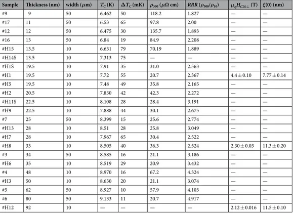
The temperature dependence of the resistivity, ρ(T), of Nb films has been investigated as a function of the thickness, d, in the range 9 d 80 nm (see Table 1). For details on fabri-cation of the films, we refer the reader to the Methods section. The ρ(T) curves shift upward, while the supercon-ducting transition temperature, TC, decreases as d is progressively reduced (Fig. 1). We have found that for filmswith 9 < d < 25 nm, the shift of the ρ(T) curves is larger than for 25 ≤ d < 80 nm (Fig. 1). The 80 nm thick film (#6), being least resistive of those measured, exhibits a room temperature (R.T.) value of ρ(T) ≈ 20 µΩ cm, approaching the Nb bulk value (15 µΩ cm)18,19. Lowering of the resistivity with thicker d suggests a gradual
reduc-tion of the film defectivity, in accordance with the behavior reported for Nb films by other groups20–22. For
<
TC T 45 K, the ρ(T) shows a plateau, due to the residual defects in the nanofilm (the nature and the influence of which will be discussed later). Starting from the thinnest films, this plateau rapidly shrinks with increasing d up to 25 nm and then attains a nearly constant value for 25 < d < 80 nm (see inset of Fig. 1).
The gradual improvement of the film quality for larger d is also deduced by the thickness dependence both of the residual resistivity ratio, RRR, here defined as the ρ(T) ratio at T = 300 K and T = 10 K, i.e. RRR = ρ300/ρ1023
and the quantity C = (RRR−1)−1, proportional to defects density in the film21. RRR grows monotonically with d,
from ~2, for d = 9 ÷ 13 nm, to ~5 at d = 80 nm (Fig. 1: inset). These values are comparable with the data reported by Lotnyk et al.23 and, for d < 40 nm, also with the data of Mayadas et al.24. Agreement with findings of Delacour
et al.21 occurs at the lowest thickness (d ≈ 10 nm). Finally, the rapid lowering of C with increasing film thickness
indicates reduction of the defect density (Fig. 2), in agreement with findings of ref.21. It is worth noting that C
Sample Thickness (nm) width (µm) TC (K) ∆TC (mK) ρ300 (µΩ cm) RRR (ρ300/ρ10) µ0HC20⊥ (T) ξ(0) (nm)
#9 9 50 6.462 50 118.2 1.827 — — #17 11 50 6.53 65 97.8 2.00 — — #12 12 50 6.475 30 135.7 1.893 — — #16 13 50 6.84 19 84.9 2.208 — — #H15 13.5 10 6.631 79 70.19 1.889 — — #H14S 13.5 10 7.313 75 — — — — #H1S 19.5 10 7.91 35 31.0 2.563 — — #H1 19.5 10 7.72 55 20.7 2.367 4.4 ± 0.10 7.77 ± 0.14 #H5 19.5 10 7.48 49 35.8 2.165 — — #H2 20.5 10 7.830 42 42.3 2.272 — — #H11S 22.5 10 8.108 28 28.4 3.191 — — #H9 22.5 10 7.888 44 30.1 2.675 — — #7 25 50 8.399 15 25.6 2.774 — — #H13 28 10 8.51 28 25.8 3.049 — — #H7 28 10 7.967 65 30.4 2.522 — — #H8 33 10 8.505 40 36.3 2.524 2.30 ± 0.03 11.3 ± 0.20 #3 34 50 8.585 16 21.1 3.186 — — #H6 35 10 8.519 29 20.9 3.432 — — #4 48 10 8.970 16 67.2 4.324 — — #H3 50 10 8.630 20 21.1 3.074 — — #5 62 50 8.927 10 57.9 4.103 — — #6 80 50 9.133 11 20.7 4.917 — — #H12 92 10 — — — — 2.12 ± 0.016 11.5 ± 0.10
Table 1. The experimentally measured properties of different Nb nanofilms. From left to right: Sample name (an S, following the number, indicates deposition on a sapphire substrate); Film thickness; width of the sample used for the electrical characterisation; TC; Superconducting transition width, ∆TC; Resistivity at 300 K;
Resistivity ratio (RR) at 300 K and 10 K; Perpendicular critical magnetic field at 0 K; coherence length in the film plane at 0 K. For resistivity measurements, 1 µA of current intensity has been sourced to all films but #7 (50 µA); #5 (10 µA and 50 µA) and #6 (50 µA).
becomes lower, for the same thickness, in those films deposited on the sapphire substrate (see Fig. 2). Possible effects of the substrate on other measured film properties will be addressed later.
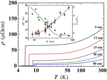
Residual resistivity (i.e. ρ10) can be used to estimate the charge carriers mean-free path, l, at T = 10 K,
assum-ing the constancy of the product ρl = 3.75 × 10⁻⁶ µΩ cm2, ρ being the bulk Nb resistivity25. Values for l range
from ≈1 nm, at the lower thicknesses, to ~9 nm at d = 80 nm (Fig. 3). Films deposited on sapphire evidence higher l values, in agreement with an expected lower defect density in the film matrix (Fig. 3). Later in our analy-sis, the thickness dependence of l will be used to extract the thickness dependence of superconducting coherence length and magnetic penetration depth.
Next, we have studied in detail the dependence of the superconducting transition temperature on film thickness. We have determined TC as the midpoint between temperatures corresponding to the 10% and the 90% of the normal
resistance value, located on the residual resistance plateau of the R(T) curve, for T > TC. The difference of those two
T values was taken as the width of the superconducting transition, ∆TC. As expected, TC decreases with decreasing
thickness, from TC 9 1. K for d = 80 nm to TC 6 5. K for ≈10 nm. For d values lower than ~13 nm, TC decreases
more abruptly, with similar TC values found for our five thinnest films (Fig. 4). Compared to TC data reported in the
literature by other groups, the TC of our films is somewhat higher for d larger than 17 nm, becoming lower for
smaller thicknesses (Fig. 4). This suggests certain level of disorder in our thinnest films. To check that, we examined the width of the superconducting transition, ∆TC, measured as 15÷30 mK, for 25 ≤ d <80 nm, increasing to
Figure 1. Temperature dependence of the resistivity for selected Nb films, with a thickness ranging from 9 nm to 80 nm. Inset: width of the plateau region (∆T), above TC, as a function of d (circles). As ∆T we have
considered the T interval corresponding to a film resistivity change of ±2.5% of ρ(T) @ 10 K. Squares: resistivity ratio at T = 300 K and at T = 10 K as a function of d. All films have been deposited on SiO2 substrates except
those, shown by yellow filled symbols, deposited on sapphire.
Figure 2. Thickness dependence of the quantity C = (ρ300/ρ10 − 1)−1. ρ300/ρ10 is the residual resistivity ratio
(i.e. RRR). All films have been deposited on SiO2 substrates except for those indicated by yellow filled circles,
www.nature.com/scientificreports/
÷
70 80 mK for the smallest thicknesses (d < 25 nm; Fig. 5). Zhao et al.20 reported a rapidly rising ∆T
C for
d < 30 nm, with multiply larger values than those measured in our films with comparable thickness (Fig. 5). These results suggest a superior quality of our superconducting Nb nanofilms at all thicknesses.
What is then the reason for observed lower TC values for d < 17 nm than was the case in ref.20? This is likely
an unwanted contribution from an oxidized Nb (i.e. NbOx) layer26, formed at the interface between the Nb film
and the SiO2 substrate, becoming progressively stronger with the reduction of d. This oxide layer decreases the
quality of the film-substrate interface, and reduces the effective Nb film thickness. Such a contribution is largely reduced on sapphire substrates, which could explain the smoother decrease of TC(d) detected by Zhao et al.20. To
verify this, we carried out a specific check, depositing 13.5 nm, 19.5 nm and 22.5 nm thick Nb films on a sapphire substrate (i.e. #H14S, #H1S and #H11S, respectively). Indeed, in those films TC was significantly higher (~0.5 K
of increase of TC for d = 13.5 nm, see yellow filled circles in Fig. 4) than in those deposited on a SiO2 substrate,
obtained during the same run (#H15 & #H1; #H9: see Table 1). The reduction of C and the increase of l, in films deposited on sapphire, is in agreement with the hypothesis of a better quality of the layer at the film-substrate interface.
Figure 3. Thickness dependence of the mean free path at 10 K. Data have been derived from the resistivity values measured at the same temperature (i.e. ρ10) for either 10 µm (blue dots) or 50 µm (red dots) wide films.
Yellow filled symbols correspond to films (10 µm wide) deposited on a sapphire substrate; all the other films have been deposited on SiO2. Continuous line is a guide for eyes.
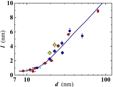
Figure 4. Thickness dependence of the superconducting transition temperature. Circles: data of the present work, for layers deposited on SiO2 (red filled) and on sapphire (yellow filled). For comparison, we have added
Another likely effect of the formed NbOx layer is that, being a conductive system of electrons in their normal
state, it is able to sink Cooper pairs from the superconducting Nb nanofilm, suppressing the condensate fraction and reducing the TC via proximity effect. This phenomenon should become more effective as the thickness of the
Nb nanofilm is reduced so that NbOx layer becomes a sizeable fraction of the Nb film thickness. Indeed, the TC(d)
curve of Fig. 4 shows a smooth decrease of TC for intermediate-to-large film thickness (i.e. for 20 d 80 nm),
which accelerates for smaller d values (i.e. at d 20 nm). The TC suppression law, due to the proximity effect, has
been derived by McMillan27 and is given by:
π = ⎛ ⎝ ⎜⎜ ⎜⎜ . ⎞ ⎠ ⎟⎟⎟ ⎟ α − T T T T 3 56 , (1) C C D C d 0 0 /
where α = dNNN(0)/NS(0) is an effective thickness of the conductive layer at the interface; TC0 = 9.22 K is the bulk
TC of Nb and TD = 277 K is the Debye temperature. The quantities NN(0) and NS(0) are the density of states in the
normal (N) and superconducting (S) layers, respectively. For simplicity, considering the ratio NN(0)/NS(0) equal
to unity, one obtains α ≅ dN. Delacour et al.21 applied Eq. (1) to fit their data set for TC(d) of Nb films on sapphire,
finding a very small effective thickness of the normal layer of dN = 0.54 ± 0.02 nm. Following the same procedure
and interpretation of Delacour et al. we obtain a satisfactory fit of our data for TC(d) using Eq. (1) and dN = 0.96
± 0.04 nm (Fig. 6). In addition, we have found an intermediate value of dN=0.76 ± 0.03 nm for the TC(d) data set
of Zhao et al.20 for films also on sapphire. We conclude that the obtained thickness of NbO
x in our case (~1 nm)
is reasonable, being comparable but larger than found in films grown on sapphire. This analysis confirms the important role played by the substrate. In particular, the absence of reactive oxygen, especially onto the substrate surface, is a mandatory requirement to deposit ultra-thin and ultra-clean Nb films, avoiding or drastically limit-ing the formation of a metallic oxide at the film-substrate interface.
At this point it is worth noting that in the presence of an overall suppression of TC(d) due to proximity effect,
the fitting function given by Eq. (1) can be subtracted from the general data set in order to amplify the visibility of the remaining oscillations of TC for decreasing d. Namely, in this range of thicknesses, one expects that TC starts
to display oscillations due to proliferating quantum size effects and shape resonances associated with confinement effects in the perpendicular direction. We have applied the aforementioned subtraction to our TC(d) data, but also
to the data of Delacour et al.21 and Zhao et al.20 where such oscillations were not considered. Remarkably, in all
cases we detected residual TC oscillations of increasing amplitude for decreasing d (shown in Fig. 7). The observed
increase of oscillations could be attributed to an incipient effect of the shape resonances when d < 20 nm. Namely, the detected oscillations of TC with amplitude of 5% in the thinnest films are very much comparable to the
theo-retical predictions for Al and Pb films of similar thickness, discussed in ref.28 (and references therein), suggesting
their quantum-confinement origin in our Nb nanofilms. As should be the case, for larger thicknesses (d > 20 nm) the TC oscillations in our films get progressively reduced in amplitude.
As the final characterization of the critical temperature in our films, we discuss the recent findings of Ivry et al.29 that T
C should exhibit an intricate dependence not only on the film thickness but also on the sheet
resist-ance, RS. Namely, Ivry et al. demonstrated a universal relationship among TC, d and RS, for films with thicknesses
in a broad range (i.e. ≈1 ÷ 103 nm) and belonging to different classes of superconducting materials29, showing
that experimental data can be well described by the relation:
Figure 5. Thickness dependence of the superconducting transition width. Circles: data of the present work, measured in films deposited on SiO2 (red filled) and on sapphire (yellow filled). Squares: data taken from Zhao
www.nature.com/scientificreports/
⋅ = −
d TC AR ,S B (2)
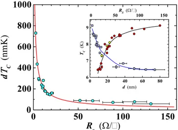
where A and B are fitting parameters, hereafter considered unitless. We have therefore investigated the behavior of TC in our films as a function of RS, to test the validity of Eq. (2). Figure 8 shows the very successful fit, yielding
A = 1350 ± 120 and B = 0.76 ± 0.05. Our B value is in excellent agreement with the result of Ivry et al. for Nb films, while our parameter A is larger29,30. This fact, in addition to the better quality of our nanofilms, is also due
to the different range of data points used for the fit compared to those considered in ref.29. The inset of Fig. 8
shows that in our case TC steeply decreases for <R0 S 20 Ω/ , and then attains an almost constant value for RS
> 50 Ω/ .
Other critical quantities and characteristic length scales of the superconducting state.
Additional information about the physical properties exhibited by the here investigated Nb films can be extracted from the behav-ior of the critical current density, JC, and the maximal magnetic field the superconducting samples can sustain, i.e. theFigure 6. Superconducting transition temperature as a function of the reciprocal film thickness. Present work (SiO2 substrate: red filled circles; sapphire substrate: yellow filled circles); Zhao et al.20 (triangles); Delacour
et al.21 (squares). Continuous lines are least-squares fit, using Eq. (1) (see text), of the different data sets. The
effective thickness of the normal layer (in nm) is represented by the corresponding α value for each curve.
Figure 7. Plot of the ratio TC/F(d) (see text) as a function of the film thickness for several Nb data sets. The
fitting function, F(d), has been calculated using the theoretically expected value of the Nb bulk transition temperature (i.e. TC0 = 9.22 K). Circles: present work; triangles: Zhao et al.20; squares: Delacour et al.21. The
upper critical magnetic field HC2. We measured the critical current at different fixed temperatures and in absence of any
applied magnetic field. We assumed as critical current the lowest I value causing the jump into the normal state in the I-V curve. The uncertainty in the critical current values was less than 1% (see the supplementary information and Figure S2). The aim is to obtain the functional temperature dependence of these quantities and then extrapolate their values at zero temperature. The dependence of the critical current density, JC, on reduced temperature, t = T/TC, for
selected films (representative of all investigated ones), is shown in Fig. 9. To model the measured JC(t) behaviour, we rely
on the Ginzburg-Landau (GL) theory, although it is formally valid only near TC. However, to recover the experimentally
well-known temperature dependence of thermodynamic critical field ∝Hc (1−t2) (as opposed to Hc ∝ (1 − t) in
standard GL theory), we employ the empirical modifications proposed by Ginzburg31 (also corresponding to the
tem-perature dependence from a two-fluid model), as already successfully used in theoretical descriptions of single-crystalline superconductors even far below TC32. As a consequence of these modifications, the GL parameter κ =
λ/ξ (where λ is the penetration depth and ξ the coherence length) becomes temperature dependent κ(T) = κ(0)/(1 + t2), the upper critical field exhibits dependence H
c2 ∝ (1 − t2)/(1 + t2), and the depairing current density becomes
pro-portional to (1 − t2)(1 − t4)1/2. For more details, we refer the reader to supplementary material.
In absence of an applied magnetic field, the measured critical current density should (nearly) correspond to the depairing current density. Assuming the above modified GL behavior of JC(T), we performed the fitting of the
Figure 8. Dependence of the product of the film thickness, d, and the superconducting transition temperature, TC, on the sheet resistance (Rs) for the investigated Nb nanofilms. The red line is the least-squares fit of the
data obtained using Eq. (2). Inset reproduces the behavior of TC (circles) and of RS (squares) as a function of
the thickness. Yellow filled symbols refer to samples deposited on sapphire substrates. Blue and black lines are guides for the eyes.
Figure 9. Normalised temperature dependence of the critical current density. Plotted curves refer to four films covering the whole range of thicknesses of the considered Nb nanofilms. Lines are the least-squares fit by the Ginzburg-Landau relation (see the equation S1 in the supplementary material) to the experimental data points.
www.nature.com/scientificreports/
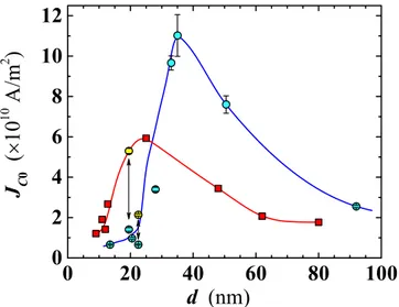
obtained data to extract JC0 for films of different thicknesses, having a lateral width of either w = 10 µm or w =
50 µm. We found a strong dependence of JC0 on both the thickness and the width. It turns out that, compared to
the Nb bulk JC0 value of 1.96 MA/cm2, our films exhibit considerably higher JC0 for thickness in the range 13 < d
< 60 nm, with a peak value ~3 and ~5.5 times higher for sample width w = 50 µm and w = 10 µm, respectively (see Fig. 10). The sizeable increase of JC0 upon narrowing the film width is related to the edge barrier effects for
vortex entry, as observed also by Il’in et al.33. Effects of the film geometry on J
C are expected when the penetration
depth becomes comparable to any dimension of film cross-section (d or w), at the crossover between depinning and depairing mechanism for the critical current. In addition, the increase of JC0 in nanofilms deposited on
sap-phire evidences once more the important role played by this substrate in improving the superconducting prop-erties of the nanofilms.
The measured critical current densities allow to estimate the penetration depth λ of the Nb nanofilms as a function of d. For type-II superconductors with thickness smaller than λ (2d < λ), holds the relation of Talantsev and Tallon34: λ πµ λ κ = = Φ + . J sf( ) H 4 (ln 0 5), (3) CII C1 0 0 3
where Φ0 is the magnetic flux quantum; µ0 the vacuum permeability and κ = λ/ξ generally assumed to be ≈1 for
Nb in the clean limit. J sfCII( ) represents the current density which generates the self field that induces vortices and itself limits the maximal current in absence of any applied magnetic field. Therefore, under the above mentioned condition, the critical current density is determined only by the fundamental lengths of the superconducting state
λ and ξ, and is independent of geometry and detailed pinning microstructure. Applying Eq. (3) to the measured values of the critical current density we have extrapolated the values of λ at the lowest accessible T by the experi-mental setup (≈4 K). The resulting thickness dependence of λ is shown in Fig. 11 together with the λ values measured in Nb films by Gubin et al., using a resonance technique22. The agreement between our data and those
of ref.22 is very good up to d ≈25 nm, with an increasing discrepancy for d ≈ 50 nm. An alternative check of the
thickness dependence of λ has been done by using the experimental mean free path l (Fig. 3) and the relation valid in the dirty limit35:
λ= . λ ⎛ξ ⎝ ⎜⎜ ⎜ ⎞ ⎠ ⎟⎟⎟ ⎟ l 0 62 , (4) L 0
where λL = 39 nm and ξ0 = 38 nm are the Nb bulk value of the London penetration depth and the BCS coherence
length, respectively. For thinner films (d 20 nm) the values of λ calculated either by Eq. (4) or Eq. (3) are com-parable while diverging, in values and behaviour for thicker films. While λ calculated by Eq. (4) preserves the likely correct d dependence and decreases towards the bulk limit, its values are more than halved with respect to those obtained in ref.22. The apparent disagreement in our λ(d) data calculated by the two methods, can be
accounted for considering that Eq. (3) is valid for 2d λ34, condition that appears to be fulfilled in our case only
below d ≈ 20 nm (Fig. 11). Finally, it is worthwhile to consider also the dependence of λ on the value of κ in Eq. (3), considering that much larger values of the GL parameter are expected in dirty films compared to single-crystalline samples. Figure 11 reproduces also the possible range of values taken by λ for 1 ≤ κ ≤ 20 in the thickness range 10 < d < 50 nm. Looking at Fig. 11 it is evident that assuming κ ≈ 1 (as was actually done in ref.34) a better agreement between the two calculation methods of λ would have been found.
Figure 10. Thickness dependence of the critical current density extrapolated at 0 K. Circles: films w = 10 µm wide; yellow filled symbols correspond to the films deposited on sapphire substrates. Squares: w = 50 µm wide. The two lines are guides for the eyes.
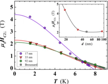
Finally, we have also studied the temperature dependence of the perpendicular critical magnetic field, HC2⊥,
for three Nb nanofilms having a thickness of 19.5 nm, 33 nm and 92 nm (#H1, #H8 and #H12, respectively). The HC2⊥ value has been determined by measuring the resistivity as a function of the applied magnetic field, at
differ-ent fixed T (Figure S3 in supplemdiffer-entary material). The experimdiffer-ental HC2⊥(T) curves for the three films are
repro-duced in Fig. 12. At a fixed T, the HC2⊥(T) has been determined as the average of the two H values corresponding
to the 10% and the 90% of the ρ(H) saturation value. The two thicker films (i.e. #H8 & #H12) exhibit practically overlapped curves. Approaching the lowest T, HC2⊥(T) tends to saturate while a small deviation from the linearity
has been detected for the thinner film (i.e. #H1) at T > 5.5 K. This fact suggests inhomogeneity effects in the film thickness and/or presence of defects due to the reduced d value, that is likely related to an interaction of the Nb film with the SiO2 of the substrate, as mentioned above in the discussion of the rapid decrease of TC in that limit.
The T dependence of HC2⊥ has been captured by a least-squares fit of the experimental values using the relation36:
Figure 11. Penetration depth as a function of the Nb film thickness. Values have been calculated by using both Eq. (3), with κ = 2.2 (spheres), and Eq. (4) valid in the dirty limit (triangles). Shown data refer to films having width w = 10 µm (blue) or w = 50 µm (red). Squares: values measured by Gubin et al.22. Dash and dotted lines
delimit the range of λ variation (for the case w = 50 µm), for κ varied between 1 (bottom line) and 20 (top line) in Eq. (3). Continuous lines are guides for the eyes.
Figure 12. Temperature dependence of the perpendicular critical magnetic field (HC2⊥). For each temperature,
the corresponding HC2⊥ value has been derived as the mean value of the applied magnetic fields corresponding
to 10% and 90% of the resistivity value at the saturation point (see Figure S3 in supplementary material). Lines are the least-squares fit of the data points by Eq. (5). For comparison, data of Broussard38 for the H
C2⊥ of a 48 nm
thick Nb film have been added to the plot. Inset: thickness dependence of HC2⊥ at 1.6 K, for the three investigated Nb films (spheres) and for the sample of Broussard38 (square) whose value, at 1.6 K, has been
extrapolated by Eq. (5) from the experimental data available down to ≈6 K. The black line serve as a guide for the eyes.
www.nature.com/scientificreports/
= − + ⊥ ⊥ H T H T T T T ( ) [1 ( / ) ] [1 ( / ) ], (5) C C C C 2 20 2 2with HC20⊥ being the value of the orthogonal upper critical magnetic field at zero temperature.
The values of HC2⊥( )T allow us to calculate the in-plane coherence length ξ T( ) of our films, extracted by the standard GL relation36: πξ = Φ ⊥ H T T ( ) 2 ( ), (6) C2 20
The Ginzburg-Landau coherence lengths at T = 0 K, ξ(0), for the three samples considered in Fig. 12, have been derived using the Eq. (6) and the HC20⊥ values extracted by the Eq. (5). ξ(0) raises from .7 8 nm for d =
19.5 nm to ≈11.5 nm for d ≥ 90 nm (see Table 1), compared to the Nb bulk value of ξ(0) = 0.74 ξ0 ≈ 28 nm.
Our results are in agreement with those reported by Trezza et al. for Nb films of comparable thickness37, and
with values measured by Broussard in a 48 nm thick Nb film38. Figure 12 reproduces the
⊥
HC2 ( )T data of ref.38 and
shows an overlapping trend with data for our two thicker films, suggesting a saturation of HC2⊥ for Nb films with d larger than 33 nm. The hypothesis has been confirmed also by the HC2⊥( )T value of the Broussard film at 1.6 K obtained through a best fit with Eq. (5) (see the inset of Fig. 12).
Finally, the thickness dependence of the superconducting coherence length in our samples has been evaluated using the experimental l values, under the validity of the dirty limit condition:
ξ(0)= .0 855 ( ) ,ξ0l (7)
where ξ0 = 38 nm is the BCS Nb bulk coherence length. The value of the coherence length at 10 K raises from ξ =
4 nm for d ≈ 10 nm, up to ξ 13 nm for d ≈ 35 nm. For larger thicknesses we observe a saturation effect albeit data points appear somewhat scattered (Fig. 13). In any case, the ξ values calculated by Eq. (7) are in very good agreement with those derived from the HC2⊥(T) measurements (Fig. 13). Finally, we note that, at d = 19.5 nm
(#H1), ξ(0) 7 8 nm evidences presence of smaller Cooper pairs, exhibiting shrinking by a factor of five com-. pared to the bulk value.
Discussion and Conclusions
The comprehensive experimental characterisation of metallic and superconducting properties of Nb nanofilms reported in this work demonstrates two different regimes depending on the thickness. For large thickness, in the range 25 nm < d < 80 nm, all measured electrical properties evolve smoothly for decreasing d. The Nb nanofilms are found to be of high quality and superconductivity has a 3D character. Around d = 25 nm, normal and super-conducting state properties display an abrupt change in their behavior. Below 25 nm of thickness, superconduc-tivity becomes progressively 2D, realizing a 3D-2D dimensional crossover. This dimensional crossover for decreasing thickness results to be particularly evident in the sudden suppression of TC, in the peaked behaviour
of the critical current density and when comparing the evolution of the penetration depth and the correlation length as a function of thickness. Approaching d = 10 nm, novel quantum phenomena start to emerge: (i) on top of the overall drop of TC, for decreasing d, remaining oscillations of TC(d) indicate incipient quantum size effects.
(ii) A factor of five enhancement of the penetration depth for the thinnest films with respect to the bulk has been Figure 13. Thickness dependence of the coherence length at zero temperature for investigated Nb films. Squares: values derived by Eq. (7) taking into account the measured mean free path (l). Spheres are the ξ(0) values calculated by the measured HC2⊥(T) and the fitting procedure described in the text.
Methods
Niobium nanofilms have been deposited at room temperature on thermally oxidized Si wafer (silicon oxide thick-ness: 300 ÷ 500 nm), by an ultra high vacuum DC sputtering system, in a base pressure of about 2 × 10⁻⁹ mbar.
Film thickness has been varied from about 9 nm to 90 nm, keeping constant the deposition rate at 0.65 nm/s (see Table 1). Scanning electron microscopy (SEM) analysis has been carried out on some films by a FEI QuantaTM 3D
FIB (Nanofacility Piemonte, INRIM).
For characterization of the electrical properties samples have been shaped in a Hall bar geometry, 1 ÷ 2 cm long, 10 µm and 50 µm wide. The resistivity, ρ(T), and the current-voltage (I–V) characteristics have been measured as a function of the temperature, in the range 4 ÷ 300 K, by a He closed cycle cryostat (Advanced Research System mod. 210 DE) equipped with two silicon diode thermometers (Lakeshore DT-670, one of which was calibrated with a maximum error of 6.3 mK) and a temperature controller Lakeshore mod. 332. Resistivity and I-V characteristics have been measured sourcing a constant current (Keithley mod. 220), monitored either by a pico-ammeter (Keithley mod. 6487 for ρ(T)) or by a multimeter (Hewlett-Packard mod. 34401 A for I-V). The voltage drop has been detected by a multimeter (Keithley mod. 2000). For the measure of ρ(T) the current sourced has been in the range 1 ÷ 50 µA. Depending on the kind of characterization, measures have been exe-cuted either with (e.g. I-V characteristics) or without T stabilization (e.g. ρ(T)). In the former case, a T stability better than 50 mK has been achieved below 15 K. In the latter approach, the variation of T during data acquisition was lower than 20 ÷ 30 mK. The superconducting transition temperature TC as well as the width of the transition
was measured by a liquid He-cryostat equipped with a silicon calibrated thermometer. For the determination of the upper critical magnetic field, HC2, a liquid 4He cryostat, Oxford Instruments Teslatron 16T has been used,
equipped with a superconducting magnet (up to 16T) and a variable temperature insert working from 300 K down to 1.5 K. The resistance values were measured by using either a PICOWATT AVS-47 AC or a Lakeshore mod. 370 AC resistance bridge.
References
1. Russo, R. et al. Performances of niobium planar nanointerferometers as a function of the temperature: a comparative study. Supercond. Sci. Techn. 27, 044028 (2014).
2. Karasik, B. S., Gaidis, M. C., McGrath, W. R., Bumble, B. & LeDuc, H. G. Low noise in a diffusion-cooled hot-electron mixer at 2.5 THz. Appl. Phys. Lett. 71, 1567–1569 (1997).
3. Semenov, A. et al. Ultimate performance of a superconducting quantum detector. Eur. Phys. J.: Appl. Phys. 21, 171–178 (2003). 4. Perali, A., Bianconi, A., Lanzara, A. & Saini, N. L. The gap amplification at a shape resonance in a superlattice of quantum stripes: A
mechanism for high Tc. Solid State Comm. 100, 181–186 (1996).
5. Bianconi, A., Valletta, A., Perali, A. & Saini, N. L. High Tc superconductivity in a superlattice of quantum stripes. Solid State Comm. 102, 369–374 (1997).
6. Bianconi, A., Valletta, A., Perali, A. & Saini, N. L. Superconductivity of a striped phase at the atomic limit. Physica C 296, 269–280 (1998).
7. Perali, A., Innocenti, D., Valletta, A. & Bianconi, A. Superconductivity of a striped phase at the atomic limit. Supercond. Sci. & Technol. 25, 124002 (2012).
8. Blatt, J. M. & Thompson, C. J. Shape Resonances in Superconducting Thin Films. Phys. Rev. Lett. 10, 332–334 (1963). 9. Thompson, C. J. & Blatt, J. M. Shape resonances in superconductors - II simplified theory. Phys. Lett. 5, 6–9 (1963).
10. Innocenti, D. et al. Resonant crossover phenomena in a multiband superconductor: tuning the chemical potential near a band edge. Phys. Rev. B 82, 184528 (2010).
11. Guidini, A. & Perali, A. Band-edge BCS-BEC crossover in a two-band superconductor: physical properties and detection parameters. Supercond. Sci. Technol. 27, 124002 (2014).
12. Bianconi, A., Innocenti, D., Valletta, A. & Perali, A. Shape Resonances in superconducting gaps in a 2DEG at oxide-oxide interface. J. of Phys.: Conf. Series 529, 012007 (2014).
13. Milosevic, M. V. & Perali, A. Emergent phenomena in multicomponent superconductivity: an introduction to the focus issue. Supercond. Sci. Technol. 28, 060201 (2015).
14. Buzdin, A. I. Proximity effects in superconductor-ferromagnet heterostructures. Rev. Mod. Phys. 77, 935 (2005).
15. Fretto, M. et al. Nano SNIS Junctions Frabicated by 3D FIB Sculpting for Application to Digital Electronics. IEEE Trans. Appl. Supercond. 23, 1101104 (2013).
16. Chen, Y. J., Shanenko, A. A., Perali, A. & Peeters, F. M. Superconducting nanofilms: molecule-like pairing induced by quantum confinement. J. of Phys. Cond. Matter 24, 185701 (2012).
17. Palestini, F. & Strinati, G. C. Systematic investigation of the effects of disorder at the lowest order throughout the BCS-BEC crossover. Phys. Rev. B 88, 174504 (2013).
www.nature.com/scientificreports/
19. Electronic Configuration & Properties of the Elements. Dean, J. A. ed., McGraw-Hill, 4 (Table 4.1) (1999).
20. Zhao, L. et al. Fabrication of Nb Superconducting Nanowires by Nanoimprint Lithography. IEEE Trans. Appl. Supercond. 25, 2200605 (2015).
21. Delacour, C. et al. Persistence of superconductivity in niobium ultrathin films grown on R-plane sapphire. Phys. Rev. B 83, 144504–8 (2011).
22. Gubin, A., Il’in, K., Vitusevich, S., Siegel, M. & Klein, N. Dependence of magnetic penetration depth on the thickness of superconducting Nb thin films. Phys. Rev. B 72, 064503–8 (2005).
23. Lotnyk, D., Komanicky, V., Bunda, V. & Feher, A. Superconductivity of niobium thin films in the BiOCl/Nb heterostructures. ArXiv:1609.02390v1.
24. Mayadas, A. F., Laibowitz, R. B. & Cuomo, J. J. Electrical Characteristics of rf Sputtered Single Crystal Niobium Films. J. Appl. Phys. 43, 1287–1289 (1972).
25. Ashcroft, N. W. & Mermin, N. D. Solid State Physics. Holt. (Rinehart & Winston publisher, New York, 1976). 26. Gershenzon, M. & Koshelets, V. Zh. Tekh. Fiz. 50, 572 (1980).
27. McMillan, W. L. Tunneling Model of the Superconducting Proximity Effect. Phys. Rev. 175, 537–542 (1968).
28. Shanenko, A. A., Croitoru, M. D. & Peeters, F. M. Quantum-size effects on TC in superconducting nanofilms. Europhys. Lett. 76,
498–504 (2006).
29. Ivry, Y. et al. Universal scaling of the critical temperature for thin films near the superconducting-to-insulator transition. Phys. Rev. B 90, 214515 (2014).
30. Ivry, Y. et al. Supplemental Material. Phys. Rev. B 90, 214515 (2014).
31. Ginzburg, V. L. Some remarks concerning the macroscopic theory of superconductivity. Sov. Phys. JETP 3, 621 (1956).
32. Müller, A. et al. Magnetization Measurements and Ginzburg-Landau Simulations of Micron-Size β-Tin Samples: Evidence for an Unusual Critical Behavior of Mesoscopic Type-I Superconductors. Phys. Rev. Lett. 109, 197003 (2012).
33. Il’in, K., Siegel, M., Semenov, A., Engel, A. & Hübers, H.-W. Critical current of Nb and NbN thin-film structures: the cross-section dependence. Phys. Stat. Sol. (C) 2, 1680–1687 (2005).
34. Talantsev, E. F. & Tallon, J. L. Universal self-field critical current for thin-film superconductors. Nat. Comm. 6, 1–8 (2015). 35. deGennes, P. G. Superconductivity of Metals and Alloys.. (Perseus Books publisher, USA, 1999; 25–26.
36. Bao, X.-Y. et al. Quantum Size Effects on the Perpendicular Upper Critical Field in Ultrathin Lead Films. Phys. Rev. Lett. 95, 247005 (2005).
37. Trezza, M. et al. Superconducting properties of Nb thin films deposited on porous silicon templates. J. Appl. Phys. 104, 083917–7 (2008).
38. Broussard, P. R. Parallel Critical Field in Thin Niobium Films: Comparison to Theory. J. Low Temp. Phys. 189, 108–119 (2017).
Acknowledgements
We thank Antonio Bianconi, Mauro Doria and Vincenzo Lacquaniti for useful discussions. We acknowledge the collaboration with Federica Celegato for AFM analysis and Sara Quercetti for the electrical properties characterization. A.P. and N.P. acknowledge financial support from University of Camerino FAR project CESEMN. We also acknowledge the collaboration within the MultiSuper International Network (http://www. multisuper.org) for exchange of ideas and suggestions.
Author Contributions
N.P., A.P. and N.D.L. conceived the experiments. M.F. and N.D.L. fabricated samples. N.P., S.J.R., M.F. and C.C. conducted the experiments, N.P., A.P., L.F. and M.V.M. analysed the results. All authors reviewed the manuscript.
Additional Information
Supplementary information accompanies this paper at https://doi.org/10.1038/s41598-018-22983-6. Competing Interests: The authors declare no competing interests.
Publisher's note: Springer Nature remains neutral with regard to jurisdictional claims in published maps and institutional affiliations.
Open Access This article is licensed under a Creative Commons Attribution 4.0 International License, which permits use, sharing, adaptation, distribution and reproduction in any medium or format, as long as you give appropriate credit to the original author(s) and the source, provide a link to the Cre-ative Commons license, and indicate if changes were made. The images or other third party material in this article are included in the article’s Creative Commons license, unless indicated otherwise in a credit line to the material. If material is not included in the article’s Creative Commons license and your intended use is not per-mitted by statutory regulation or exceeds the perper-mitted use, you will need to obtain permission directly from the copyright holder. To view a copy of this license, visit http://creativecommons.org/licenses/by/4.0/.