Università degli Studi di Ferrara
DOTTORATO DI RICERCA IN
FISICA
CICLO XXVII
COORDINATORE Prof. Vincenzo Guidi
AN INNOVATIVE CYLINDRICAL MAGNETRON SPUTTERING SOURCE FOR THE DEPOSITION OF HIE-ISOLDE SUPERCONDUCTING Nb/Cu QWRs
Settore Scientifico Disciplinare FIS/03
Dottorando Tutore
Dott. Daniel Adrien Franco Lespinasse Prof. Vincenzo Palmieri
_______________________ _________________________ (firma) (firma)
iii
ACKNOWLEDGEMENTS
There are several special people that have been important until this point of my life. Some of them, linked to my profession. First of all, I would like to thank my parents for the support, love, education, advises that, for sure, have helped me to be focused on right decisions. To my sister and her friendship, love and one of my motivations, my nice Nicole…. that even far away makes me feel at home when I see her.
Of course I want to thank my uncles Robert and Regis and my aunts Jocelyne and Aida. Some of them are my godfathers, but actually they are as my seconds parents. Thanks to my cousins Regis and Diane, that forever will be a model to follow.
I cannot find words to express my gratitude to my friend Andrea who has always given me her friendship, help and support; for sure my experience would be different without you.
It is with immense gratitude that I’d like to thank for the support, protection, help an advices, my professor Lazlo Sajo.
This thesis would not have been possible without my professor Enzo Palmieri for being an ambitious and wise guide besides being a great person.
Many thanks to Sergey Stark, Anna Maria Porcellato and Antonio Rossi for having introduced me to the cryogenics world.
Special thanks to Silvia, for their patience and availability not only in matters of work. I share the credit of my work with Giorgio Keppel, for being an excellent supervisor and friend and for sharing his knowledge with me.
Thank you very much to Hanna for her help during the SEM analysis. To Alex for his availability during the magnetron mounting and Fabrizio during the cavity cleaning.
I am indebted to my many colleagues who supported me in these three years, Vlada, Alessio Oscar, Cristian, Diana, Giovanni, Manuel, Nicolò.
I want to thank my old (Lorena, Nunzio, Elena and Damiano) and new roommates (Alice, Edoardo and Mariella) to be my family in Italy and to make me feel part of you culture.
To my brother Winder, por su calor humano y darle un toque de musicalidad a la vida en momentos buenos y malos. Thanks to Michela, for her friendship, and for each word she taught me. Everybody will be on my mind and heart forever.
iv
GENERAL CONTENT
ACKNOWLEDGEMENTS ... iii
GENERAL CONTENT ... iv
FIGURE CONTENT ... viii
TABLE CONTENT ... xii
LIST OF ACRONIMS ... xiii
ESTRATTO ... xiv
ABSTRACT ... xv
Chapter 1. ... 1
INTRODUCTION ... 1
Chapter 2. ... 5
ION BEAM ACCELERATOR FACILITIES ... 5
2.1. Isolde facility ... 6
2.2. REX-ISOLDE ... 7
2.3. HIE-ISOLDE ... 8
Chapter 3. ... 9
BASES OF SUPERCONDUCTIVITY ... 9
3.1. General properties of superconductors ... 9
3.2 Coherence length in superconductors... 13
3.3.London Penetration depth ... 13
3.4.The skin effect in normal conducting case ... 15
3.5 superconducting cavities ... 16
3.6.QWR cavities ... 19
3.7 Niobium properties ... 20
3.8.Nb and superconducting cavities ... 21
3.9 Residual Resistivity Ratio (RRR)... 22
v
3.11 Bulk cavity Q-drop ... 26
3.11.1. Low Field Q-slope ... 28
3.11.2. Medium Field Q-slope... 30
3.11.3. High fields Q-slope ... 30
3.12 Hot spot and large grain cavities ... 31
3.13. Thin film and special cavities Q drop ... 31
3.14 Limitations on SRF Cavities ... 33 3.14.1 Q-disease ... 33 3.14.2 Multipacting ... 34 3.14.3 Field emission... 35 3.14.4 Thermal breakdown ... 36 Chapter 4. ... 38
THIN FILM DEPOSITION ... 38
4.1 Sputtering ... 38
4.2 Sputtering mechanism ... 40
4.3. DC Magnetron sputtering ... 41
4.4. Balanced and unbalanced magnetrons ... 43
Chapter 5. ... 46
THE VACUUM SYSTEM ... 46
5.1. 3D drawing of the vacuum chamber ... 46
5.2. The cathode ... 49
5.3. The magnetic field configuration ... 50
5.3.1. Spiral path with plastimag ... 51
5.3.2. “U” Path with permanent magnets ... 52
5.4. The rotation system ... 53
Chapter 6. ... 56
vi
6.1. Materials and equipment ... 56
6.2. Methodology ... 56
6.2.1 Magnetic field configuration ... 57
6.2.2. Small cathode configurations ... 57
6.2.3. Deposition of Niobium onto copper quartz ... 59
6.2.4. Vacuum ... 60
6.2.5 Baking ... 61
6.2.6. Pre-sputtering ... 62
6.2.7. Sputtering of niobium onto quartz samples ... 63
6.3. Characterization techniques ... 64
6.3.1. Thickness measurements ... 64
6.3.2 Residual Resistance Ratio and Critical Temperature ... 65
6.3.3 Scanning electron microscope SEM... 68
6.4. Deposition of QWR ... 68
Chapter 7. ... 72
THE RF SYSTEM ... 72
7.1 Cryostat design ... 72
7.2 RF generalities and test system ... 77
7.3. RF system ... 78
7.4. RF measurement ... 80
Chapter 8. ... 84
RESULTS AND ANALYSIS... 84
8.1 Spiral path with plastimag ... 84
8.1.1 Stainless steel onto quartz samples/copper strips ... 84
8.1.2 Niobium onto quartz samples ... 96
8.2. “U” Path with permanent magnets ... 111
vii
8.3.1. Nb onto quartz samples ... 116
8.3.2 Quarter Wave Resonator deposition... 123
Chapter 9. ... 132 CONCLUSIONS ... 132 Chapter 10. ... 134 REFERENCES ... 134 APPENDIX A ... 142 APPENDIX B ... 150 APPENDIX C ... 152
viii
FIGURE CONTENT
Figure 2.1 The ISOLDE facility [8] ... 7
Figure 2.2 REX ISOLDE scheme [6]. ... 8
Figure 3.1.Meissner effect. ... 10
Figure 3.2. Critical field versus temperature for some superconducting elements [13]. ... 11
Figure 3.3. Magnetization versus magnetic field for superconductors type I. ... 11
Figure 3.4. Critical magnetic field for superconductors type II. ... 12
Figure 3.5 Classification of accelerating structures. [13] ... 16
Figure 3.6. Low and high ß cavities [25]. ... 20
Figure 3.7 Typical R (T) curves for Nb samples of different purity [22]. ... 23
Figure 3.8.Example of typical Q vs Eacc at 1,7 K of niobium coating on copper cavities of 1,5GHz [27]. ... 25
Figure 3.9 The Q factor versus accelerating field for the best Nb-Sputtered Cu 1,5 GHz cavity fabricated at CERN [28] ... 26
Figure 3.10. Comparison of Q drops between thin films and Nb bulk cavities ... 27
Figure 3.11 Low, medium and high field Q-slopes ... 28
Figure 3.12. 2 Bilayer system made of the bulk niobium (SC 2 ) and of an over-layer of a superconductor (SC 1) with poorer superconducting properties. ... 29
Figure 3.13 Test result of the single crystal cavity at Jefferson laboratory [57] ... 32
Figure 3.14. Performance limitations regarding the quality factor Q or the accelerating electric field E in the Q vs (E) curve [57]. ... 33
Figure 3.15 Schematic examples for multipacting (MP): (a) 1st order MP, (b) 2nd order MP, (c) two point MP [38]. ... 34
Figure 3.16 a) Temperature map from the heating of impacting field emitted electrons b) Calculated field emitted electron trajectories in a three-cell 1.5 GHz cavity operating at E pk=50 MV/m [41]. ... 35
Figure 4.1 Sputtering deposition. In DC diode sputtering system, Ar is ionized by a potential difference, and this ions are accelerated to a target. After impact, target atoms are released and travel to the substrate ... 39
Figure 4.2. Interactions of ions during the deposition. ... 40
Figure 4.3. Magnetron sputtering technique. ... 42
Figure 4.4.Cross section drawing of the conventional balanced magnetron. ... 44
ix Figure 5.1. 3D drawing of the vacuum chamber. Left: Front view of the chamber assembled. Right:
Cross sectional view of the vacuum chamber. ... 46
Figure 5.2 Scheme of the vacuum chamber assembled [33]. ... 48
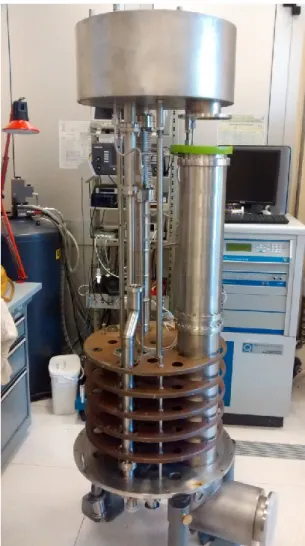
Figure 5.3. Vacuum system assembled. ... 49
Figure 5.4. Procedure used in the construction of the Nb. ... 50
Figure 5.5. Niobium cathode. ... 50
Figure 5.6. 3D drawing of the first configuration of magnetic field. B) Neodymium- Iron –Boron placed along the double spiral path. ... 52
Figure 5.7. Second configuration of magnetic field. ... 53
Figure 5.8. Rotation system. ... 54
Figure 6.1 a) Stainless steel test cathode, b) top view of the test cathode. ... 58
Figure 6.2 Magnetron placed on the vacuum chamber during the sputtering process. ... 58
Figure 6.3 Ultra sonic bath used to clean quartz samples. ... 59
Figure 6.4. a) Sample holder b) sample holder on the QWR cavity. ... 59
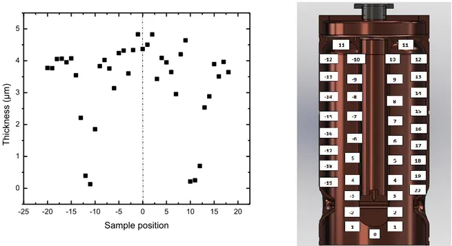
Figure 6.5. Sample positions on quarter wave resonator cavity. ... 60
Figure 6.6. QWR during the mounting on the vacuum chamber. ... 60
Figure 6.7. Baking controller. ... 61
Figure 6.8. Resistors and thermocouples placed on the vacuum chamber. ... 62
Figure 6.9. Niobium magnetron placed on the top of the vacuum chamber. ... 63
Figure 6.10. Vacuum system during the deposition... 64
Figure 6.11. Dektak 8 Profilometer used to measure the thickness of quartz samples. ... 65
Figure 6.12. Scheme of four point method. ... 66
Figure 6.13. Measuring system layout [43]. ... 66
Figure 6.14. a) Resistive sample holder. B) Helium Dewar. ... 67
Figure 6.15. QWR cavity during the mounting on the vacuum chamber. ... 69
Figure 6.16. IR lamps test before the vacuum chamber closing. ... 69
Figure 6.17. High pressure rinsing. ... 70
Figure 6.18. QWR cavity during Nb/Cu tuning plate mounting. ... 71
Figure 7.1 Top view of the cryostat flange. ... 73
Figure 7.2 Upside down of the cavity stand during the cryostat mounting. ... 74
Figure 7.3 Thermometers during their mounting on the cryostat stand. ... 74
Figure 7.4 Cryostat holder structure during the construction. ... 75
x
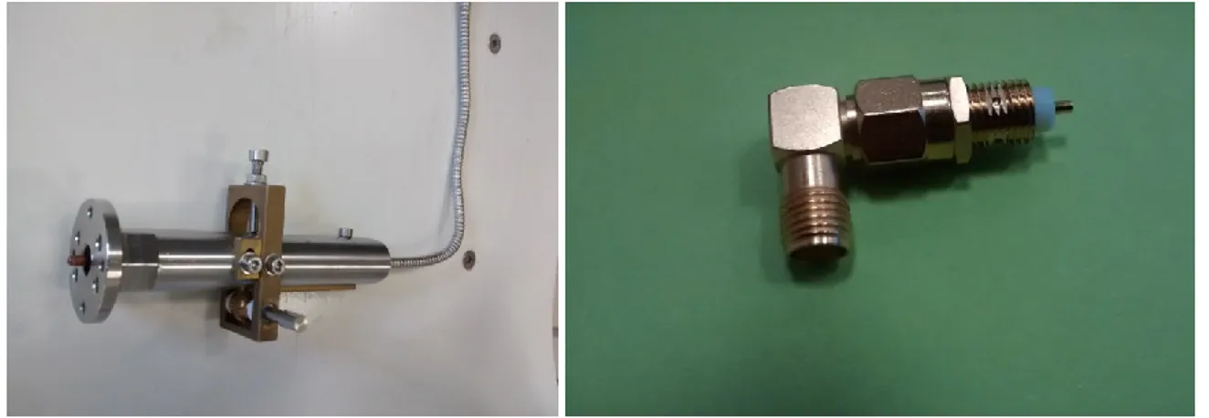
Figure 7.6. Coupler and pick-up for the quarter wave resonator cavity. ... 78
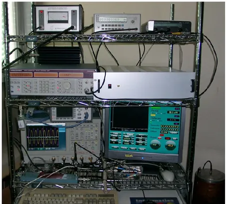
Figure 7.7. Measurement system for cavity testing [61]. ... 79
Figure 7.8. Measurement circuit for cavity characterization [61]. ... 80
Figure 7.9. On the left side the pick-up antenna and on the right side the coupler antenna, both during the mounting. ... 81
Figure 7.10. Temperature versus time during the cryostat cooling. ... 82
Figure 8.1 Deposition 1.Thickness vs sample position of stainless steel onto quartz samples. ... 85
Figure 8.2 Copper strips deposited in RUN 1. a) Before and b, c) After stripping test. ... 86
Figure 8.3. Construction of the C magnetic configuration ... 88
Figure 8.4. Argon plasma generated by: a) NdFeB cylindrical magnet in vertical position, b) NdFeB cylindrical magnet in horizontal position, c) Curve with plastimag and NdFeB cylindrical magnet in vertical position. ... 89
Figure 8.5 D top magnetic configuration. ... 89
Figure 8.6. Argon plasma produced by different top magnetic confinement. Configurations differs in the amount of magnetic material used. ... 90
Figure 8.7. a) F Magnetic confinement, b, c, d) argon plasma generated by fourth magnetic confinement. ... 91
Figure 8.8. Deposition 2.Thickness vs sample position of stainless steel onto quartz samples. ... 92
Figure 8.9. Copper strips deposited in RUN 2. a) Before and b) After stripping test... 93
Figure 8.10. Deposition 3.Thickness vs sample position of stainless steel onto quartz samples. ... 93
Figure 8.11. Copper strips deposited in RUN 3,a) before and b, c) after stripping test. ... 94
Figure 8.12. Deposition 4.Thickness vs sample position of stainless steel onto quartz samples. ... 94
Figure 8.13. Copper strips deposited in RUN 4,a) Before and b, c) After stripping test. ... 95
Figure 8.14. Deposition 5.Thickness vs sample position of stainless steel onto quartz samples. ... 96
Figure 8.15. Deposition 1.Thickness vs sample position of niobium onto quartz samples ... 97
Figure 8.16.First niobium deposition. Residual Resistivity Ratio in function of the thickness for quartz samples placed in different positions along the cavity. ... 98
Figure 8.17.Superconducting transition of sample placed in position 3 of the QWR. ... 100
Figure 8.18. IR lamp placed inside the central electrode of the QWR ... 101
Figure 8.19. Deposition 2.Thickness vs sample position of niobium onto quartz samples. ... 101
Figure 8.20. Second niobium deposition. Residual Resistivity Ratio in function of the thickness for quartz samples placed in different positions along the cavity. ... 102
xi
Figure 8.22. Deposition 3.Thickness vs sample position of niobium onto quartz samples. ... 104
Figure 8.23. Third niobium deposition. Residual Resistivity Ratio in function of the thickness for quartz samples placed in different positions along the cavity. ... 105
Figure 8.24. RRR vs sputtering power of Nb sample in position 15. ... 106
Figure 8.25 Critical temperature vs RRR for a sample located in the 15th position. ... 107
Figure 8.26 Thickness vs sample position using different parameters of process, from Run 4 to Run 7. ... 108
Figure 8.27. RRR vs power for a sample in position 15, using different parameters. ... 110
Figure 8.28. Critical temperature vs RRR for a sample located in the 15th position. ... 110
Figure 8.29. Thickness vs. sample position using different parameters of process, from Run 8to Run 10. ... 111
Figure 8.30.a) 3D drawing of second magnetic confinement, b) 3D drawing of second magnetic confinements inside the niobium cathode. ... 112
Figure 8.31. Lateral view of argon plasma produced by the modification of magnets placed on the extreme of the magnetic. ... 115
Figure 8.32.Lateral view of argon plasma produced by two curves of magnets placed on the opposite sides of the SS tube. ... 116
Figure 8.33. a) Lateral view of 3D drawing of final magnetic confinement b) Lateral view of 3D drawing of final magnetic confinements inside the niobium cathode. ... 117
Figure 8.34. Run 1.Thickness profile of quartz samples deposited with niobium, using the definitive magnetron confinement... 118
Figure 8.35. Run 2.Thickness profile of quartz samples deposited with niobium, using the definitive magnetron confinement... 120
Figure 8.36. Morphology of the niobium samples sputtered at 30Kw for 30 min... 122
Figure 8.37. QWR cavity before and after the Nb deposition. ... 124
Figure 8.38. Nb/Cu QWR cavity after the high pressure rinsing. ... 124
Figure 8.39.Cavity search at resonant frequency. ... 126
Figure 8.40.Oscilloscope signal during the multipacting conditioning. ... 126
Figure 8.41. First measurement of Q vs Eacc of Nb/Cu cavity. ... 127
xii
TABLE CONTENT
Table 1 Niobium properties ... 21
Table 2 Materials and equipment used in this project ... 56
Table 3. Parameter used to test the configuration of magnetic field. ... 57
Table 4. Parameters used to perform the Pre-sputtering process. ... 63
Table 5. Parameters used to perform the pre-sputtering process of the QWR cavity. ... 70
Table 6. Parameters used to perform the magnetron sputtering process of the QWR cavity. ... 70
Table 7 Parameters used to perform the Run 1 ... 84
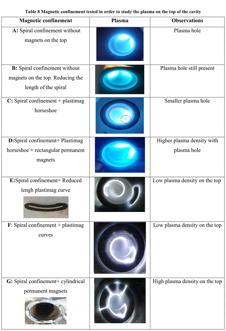
Table 8 Magnetic confinement tested in order to study the plasma on the top of the cavity ... 87
Table 9 Parameters used to perform the Run 2. ... 92
Table 10 Parameters used to perform the Run 5. ... 95
Table 11 Parameters used to perform Run 1 of niobium onto quartz samples. ... 97
Table 12 Parameters used to perform the Run 3 of niobium onto quartz samples. ... 104
Table 13 Parameters used in Run 4, 5 and 6 for depositions of niobium onto quartz samples. ... 106
Table 14. Parameters used to perform Run 8,9 and 10 for niobium onto quartz samples ... 109
Table 15 Magnetic confinements test to study the plasma on the top of the cavity with the U path ... 113
Table 16. Parameters used to perform the first Run using the definitive magnetic confinement. ... 118
Table 17. Superconductive properties of Nb onto quartz samples, using the definitive magnetic confinement. ... 119
Table 18. Parameters used to perform the second test deposition, using the definitive magnetic confinement. ... 120
Table 19. Run 2.Superconductive properties of Nb onto quartz samples, using the definitive magnetic confinement. ... 121
Table 20. Parameters used to perform the first sputtering over the copper QWR. ... 123
Table 21. Decay results of first RF measurement. ... 127
xiii
LIST OF ACRONIMS
SC: Superconductive/Superconducting.
ISOLDE: The On-Line Isotope Mass Separator. QWRs; Quarter Wave Resonators.
CERN: European Organisation for Nuclear Research. INFN: National Institute of Nuclear Physics.
LNL: National Laboratory of Legnaro (Italy). SS: Stainless Steel.
RRR: Residual Resistivity Radio. The RRR is the residual resistivity radio that indicates the level of
purity in superconductive materials.
Tc: Critical temperature.
SEM: Scanning Electron Microscope. NeFeB: Neodymium Iron Boron. PVC: PolyVinyl Chloride. RF: Radio Frequency.
SLAC: Standford Linear Accelerator Center. ALPI: In italian (Acceleratore Lineare Per Ioni). Eacc: Accelerating field
xiv
ESTRATTO
Nell'ambito del progetto Eucard è stato realizzato, in collaborazione con il CERN, l' R&D della tecnica di magnetron sputtering sulla geometria della cavità HIE-ISOLDE, come metodo alternativo per depositare film sottili di niobio. Nello specifico, presso i LNL dell'INFN è stata testata una nuova sorgente di campo magnetico per depositare un film sottile di niobio uniforme sul risonatore a quarto d'onda. La metodologia ha previsto tre fasi distinte. La prima fase, in cui un prototipo di cavità ed un catodo di prova sono stati usati per depositare acciaio inossidabile su quarzo. Lo scopo dell’utilizzo dell’acciaio è stato trovare i giusti parametri di sputtering e anche per analizzare l’uniformità del film. In questa prima fase sono stati testati diversi confinamenti magnetici che hanno permesso l’ottimazione della deposizione. Parallelamente è stata effettuata la deposizione di acciaio inossidabile su strisce di rame per realizzare il test di strippaggio come metodo per analizzare la presenza di zone non depositate. Nella seconda fase ci si è concentrati sulla deposizione di film sottile di niobio su campioni di quarzo posti lungo il risuonatore al fine di migliorare le proprietà superconduttive, specificamente Rapporto Resistività Residuo (RRR) e la temperatura critica (Tc).
Tuttavia, altri confinamenti magnetici sono stati testati per mantenere l'uniformità del rivestimento. È stata studiata l'influenza sulle proprietà superconduttive di due parametri principali del processo di sputtering: la potenza e la temperatura del substrato. Dopo aver impostato i parametri di deposizione, è stato utilizzato un confinamento magnetico definitivo per depositare la vera QWR in rame. Allo scopo di analizzare la performance della cavità ai campi RF è stata necessaria la progettazione, costruzione e installazione di un criostato. Infine, è stata trovata una nuova sorgente magnetica per depositare un film sottile di niobio uniformemente su cavità Quarto d’onda. Si è riscontrato che aumentando la temperatura del substrato e la potenza dello sputtering, la temperatura di transizione del film sottile di niobio era intorno 9,3K ed è stato ottenuto un RRR massimo di 61. Solo 30 min. sono stati necessari per depositare il film con una uniformità di 2 ± 1 micron lungo la cavità. I risultati del SEM hanno permesso di analizzare la microstruttura del film di niobio. Grani più grandi sono stati trovati sul conduttore interno, più vicino alla sorgente magnetron. Inoltre un criostato di prova è stato costruito con successo per misurare le prestazioni RF; il sistema può essere utile per effettuare misure a 4,2 e 1,8 K. La prima cavità QWR depositata con il magnetron sputtering è sotto le specifiche del CERN; è stato misurato un Q massimo di 2e8 e un campo accelerante di 2MV/m; tuttavia come
primo risultato è estremamente importante per partire con la fase di ottimazione. Alcuni parametri saranno cambiati per migliorare le prestazioni e spingere la comunità SRF ad utilizzare la tecnica magnetron sputtering come un metodo economico per depositare cavità superconduttrici in tempi brevi.
xv
ABSTRACT
In the framework of Eucard project, it has been carried out, in collaboration with CERN, the R&D on magnetron sputtering deposition on the HIE-ISOLDE cavity geometry, as an alternative method to deposit niobium thin films. In this research a new magnetron configuration source was tested at the National Institute of Nuclear Physics (INFN-LNL), in order to deposit a uniform niobium thin film onto copper superconducting Quarter Wave Resonator cavities. The methodology was divided in three. A first part, in which a test dummy cavity and a test cathode were used in order to deposit stainless steel onto copper quartz. The purpose of the use of steel has been finding the right parameters of sputtering and also to analyze the uniformity of the film. In this first phase it have been tested several magnetic confinements, which allowed the optimization of the deposition. In parallel it was performed the deposition of stainless steel onto copper strips, to realize the stripping test as a method to analyze the uniformity of the film. The second part was focused on the deposition of niobium thin film onto quartz samples placed along the resonator to improve the superconducting properties, specifically Residual Resistivity Ratio (RRR) and Critical Temperature (Tc); nevertheless
other magnetic confinements were tested to maintain the uniformity of the coating. It was studied the influence on superconducting properties of two principal parameters of the sputtering process: the power and the substrate temperature. After setting the deposition parameters, a definitive magnetron confinement was used to deposit the real copper QWR. The RF performance was also measured after the design, construction and installation of a test cryostat. Finally, it was found the magnetic source to deposit a niobium thin film uniformly over QWR cavities. Increasing the substrate temperature and the sputtering power, the transition temperature of the niobium thin film was around 9,3K and it was obtained a maximum RRR of 61. Only 30 min were necessary to deposit the film with a uniformity of 2±1 µm along the cavity. SEM results allowed to analyze the microstructure of the niobium film. Bigger grains were founds on the inner conductor closer to the magnetron source. In addition a test cryostat was successfully built in order to measure the RF performance; the system can be useful to perform measurements at 4.2 and 1.8 K. Respect to the RF performance the first Nb/Cu cavity is under the specifications of CERN with a maximum Q value of 2e8 and an accelerating field of
2MV/m; however this first result is extremely important to start with the optimization phase. Some parameters will be changed in order to improve the performance and push the SRF community to use the magnetron sputtering technique as an economical method to deposit superconducting cavities in short times.
xvi
To my parents Daniel and Gislaine and my Sister Eliane. They have given me the motivation, support and the force necessary to reach each one of my goals.
1
Chapter 1.
INTRODUCTION
Superconducting Quarter Wave Resonators (QWRs) take an important place in the construction of several particle accelerators, and for this reason it has been for years a relevant research topic for the superconducting cavity community.
Many research institutions have studied the sputtering technology applied to complex substrates. The development of the deposition of Niobium onto copper cavities started at CERN from 1980 [1], as a method to replace bulk cavities. Then, at Legnaro National Laboratories (LNL), since 1987 it has been studied the bias diode sputtering in order to deposit Niobium onto copper QWRs for the construction of ALPI accelerator, obtaining positives results: good film uniformity and good performance but lower deposition rates in comparison with other techniques such as magnetron sputtering technique [2].
Nowadays in order to increase the beam energy, QWR cavities with accelerating field of at least 6MV/m for 10W maximum power dissipation and at least 5e8 of Q value, are required to be
placed in the HIE-ISOLDE linac at CERN. This requirements were reached by CERN with the bias diode with long times of deposition [3]. For this reason, it is necessary the parallel R&D on going at CERN and LNL in the quest for higher performances.
The magnetron sputtering is a deposition technique widely used in the thin film industry, however with this method the uniformity of the film is generally not easy to control; it is a real challenge to use this technique for the coating of really complex form as having QWRs substrates.
The aim of this investigation is to find a magnetron configuration source to deposit the cavities uniformly, in short times (40min and not 40 hours) and low cost, having a good superconducting performance.
In order to carry out the first stage of this study, it was necessary to develop and realize these topics: the construction of a vacuum system with a cathode adapted to the shape of the QWR, the
2
construction of a stainless steel test cavity and also a stainless steel test cathode in order to study the magnetic field configuration, the study of magnetic field lines using the 2D Finite Element Method (FEM) software, the construction of the magnetron body and the deposition of stainless steel thin films onto quartz samples to study the uniformity along the cavity.
The second stage of this investigation was focused on the setting of the process parameters and the upgrade of the magnetic field configuration. In this part, a double wall niobium cathode was built to carry out the niobium depositions onto quartz samples. The Process parameters were studied rigorously to improve the superconducting properties of the film such as residual resistivity ratio and the critical temperature.
The next part of the research was focused on the design and construction of the 1,8/4,2K QWR cryostat and the RF transmission line, in order to study the performance of the cavity at RF fields. Last part of this study was the deposition of the real copper QWR cavity of ISOLDE type and the measurement of the RF performance.
This work has been financed by the V group of INFN in the framework of the experiment MARTE. The phases of mounting the vacuum system and all the chemistry/electrochemistry required for the surface treatments of the system has been partially financed by the European Union in the Seventh Framework Programme FP7/2007- 2013 of the contract EuCARD GA 227579, within the work package WP10.
The results of this work has been patented by INFN with the Italian application ….*
3
PHD. Thesis Construction of an innovative cylindrical magnetron sputtering for ISOLDE SPC Nb/Cu QWRs cavities HIE-ISOLDE Particle accelerator General particle accelerator ISOLDE proyect Bases of superconductivity RF Superconductive cavities RF superconductive cavities Nb cavities Nb/Cu cavities QWRs cavities Niobium properties Deposition of the film Sputtering Diode Sputtering Magnetron sputtering Vacuum system Vacumm chamber schemes cathode Magnetron Experimental method Materials and equipments Experimental procedure Magnetron simulations Chemical treatments Measurements Thickness RRR and Tc Q value and Eacc Film caracterization Results and analysis Conclusions The RF system
5
Chapter 2.
ION BEAM ACCELERATOR FACILITIES
The normal conductive particle accelerators have been first conceived in the 1930s, in order to supply charged particles to be investigated in many topics of particle physics. An accelerator can increase and speed up a beam applying electric fields, and also can focus the particles with magnetic fields.
Generally, in order to accelerate the protons, an electric field strips hydrogen nuclei of their electrons, then the electric fields switch from positive to negative at a specific frequency, pulling charged particles forwards along the accelerator. To ensure the particles in closely spaced bunches, the frequency is controlled.
In order to accelerate beams radio frequency (RF) cavities and magnets are needed. The RF cavities are metallic chambers spaced at intervals along the accelerator, they are shaped in order to resonate at determined frequencies, allowing radio waves that can interact with passing particle bunches. Each time the beam passes, the electric field is transferred to the particles. It is important that the particles cannot collide with the molecules of gases, because the beam is in an ultrahigh vacuum environment. Also various types of magnets are used in an accelerator. Dipole magnets, are used to bend the path of a beam or to focus it. Around the collision point are placed particle detectors in order to reveal the particles [4].
Depending on its shape and the path of the particles, accelerators can be classified as circular accelerator, where the particles travels around a loop, or linear accelerator if the beam of particles travels in a straight line, from one end to the other.
In 1964 Fairbank, Schwettman and Wilson at Standford Linear Accelerator Center (SLAC), start the acceleration of electrons with superconducting RF structures. In this experiment 80 keV electrons were accelerated by a lead-plated onto a 3 cell of copper, reaching an energy of 500 keV. Form this test it was demonstrated that a multicell accelerating structure could be operated at high accelerating gradients (3MeV/m) and Q’s of 1e8. From this experiment it was also demonstrated that
6
Nowadays a big number of accelerators has been used in order to reach higher energies and the type of particles depends of each experiment [4].
2.1. Isolde facility
The on-line isotope mass separator ISOLDE, is an accelerator used for the production of a big amount of radioactive ion beam that can be used or studied in the field of materials sciences, solid state physics, nuclear physics, atomic physics and life sciences. ISOLDE itself, is a multidisciplinary activity that contributes on accelerator development, silicon detectors and data processing, and simulations for beam-detector interactions.
ISOLDE is a source of low-energy beams of radioactive nuclides, with unstable neutrons. This accelerator can allows the study of many atomic nuclei, including the most exotic species.
This facility is located at the Proton-Syncotron Booster (PSB) at CERN, the European Organization for Nuclear Research. ISOLDE project has collaborators around the world and its principal members are Belgium, Denmark, Finland, France, Germany, Greece, India, Ireland, Norway, Romania, Spain, Sweden and United Kingdom [6].
At ISOLDE, a target can be irradiated with a proton beam from the PSB at 1,4 GeV and at 2µA of intensity to produce radioactive nuclides by spallation, fission or fragmentation. After the nuclear reactions the volatile nuclear products are extracted as a radioactive ion beam that could reach the highest intensities available all over the world. The accelerator has produced more than
600 isotopes with half-lives bellow to millisecond of around 70 elements (Z= 2 to 88). [7].
7
Figure 2.1 The ISOLDE facility [8]
2.2. REX-ISOLDE
The post accelerator REX-ISOLDE is a facility built to accelerate radioactive ion beam of higher energies such as light medium mass nuclei for reactions with energies up to 3,1 MeV/u. REX-ISOLDE has already accelerated several species of radioactive ions. This accelerator has been upgraded to provide the maxim um energy of 5.5MeV/u.
Nowadays the Radioactive Ion Beams (RIBs) are accelerated to high energies by a normal conducting linac, starting with the ion charge impulse. The REX-ISOLDE scheme is shown in Figure 2.2. The system is formed by a Penning trap (REXTRAP), a charge breeder (REXBIS) and an achromatic mass separator. The normal conducting accelerator has been designed with an accelerator voltage for a corresponding mass/charge ratio (A/q) of 4.5 and it delivers a final energy of 3 MeV/u for A/q < 3.5 and 2.8 for A/q < 4.5. The first accelerator stage is provided by a 101, 28 MHz Radio Frequency Quadrupole (RFQ) which takes the beam from 5 keV/u up to 300 keV/u. That beam is re-bunched into the 101,28 MHz drift tube (IH) structure to increase the energy to 1.2 MeV/u. To give
8
further acceleration to 2.2 MeV/u and finally a 202.58 MHz three split ring cavities are used, and in order to vary the energy from 2 to 3 MeV/u a 9 gap IH cavity is used [8].
Figure 2.2 REX ISOLDE scheme [6].
2.3. HIE-ISOLDE
The HIE-ISOLDE project is part of the European nuclear physics strategy that has been created to expand the physics program in comparison with the REX-ISOLDE. Its operation can help to understand many scientific cases astrophysics and physics structure. The aim of the project is to increase the energy and the intensity of the delivered radioactive ion beam (RIB), filling the requests for a more energetic accelerated beam using superconducting (SC) linacs based on Quarter Wave Resonators (QWRs) cavities.
The development of this project started in 2008, and has been focused on the improvement of the high β cavity (β = 10.3%), for which it has been decided to apply the Nb sputtered onto Cu substrates technology. The SC linac has been designed to have an effective accelerating voltage of at least 39.6 MV, with an average synchronous phase φs of 20 deg. It is necessary to reach this voltage to achieve a final energy of at least 10MeV/u and a relation A/q= 4.5. Due to the steep variation of the ions velocity it is also necessary to have at least two cavity geometries, thereby the acceleration will be efficient throughout the whole energy range. 32 cavities are needed in order to have a full acceleration voltage and the geometry of these cavities can be of two types: low ß (β0 = 6.3%) and high ß (β0 = 10.3%). The “ß” cavities works with the fundamental beam frequency of 101, 28 MHz. The design was chosen to reach 6MV/m with a consumption of power of 7 W per low ß cavities and 10 W per high ß cavities [9].
9
Chapter 3.
BASES OF SUPERCONDUCTIVITY
3.1. General properties of superconductors
In 1911 H. Kamerling Onnes, studied the electrical resistance of mercury with the temperature observing that the resistance dropped sharply to zero at a temperature of 4,2K. The same properties were later discovered in some other metals. The phenomenon was named “superconductivity” and the corresponding metals were called “superconductors”.
The temperature at which the resistance is close to zero is called critical temperature Tc and it
is different in each material with superconductive properties. The highest critical temperature between pure metals is shown by niobium, Tc=9,25K; and the lowest has been found by tungsten, Tc=0,0154K.
However these are both low temperatures and the temperature range is very wide, since the two extremes differ by about a factor of a thousand.
K. Onnes in 1914, has carried out subsequent investigations about superconductive properties. He has shown that superconductivity can be destroyed not only by increasing the temperature and also by applying a sufficiently strong magnetic field. The critical field (Hc) in which the
superconductivity is destroyed decreases with the increment of temperature. The following formula describes empirically the dependence Hc (T).
𝐻𝑐(𝑇) = 𝐻𝑐(0)[1 − (𝑇
𝑇𝑐)2 ] (3.1)
Also the superconductivity can be destroyed by a strong electric current. If the superconductor is not too thin, the magnetic field produced by a critical current must be equal to zero at the surface of a superconductor.
Meissner and Ochsenfeld in 1933, have discovered another superconductive properties. If a metal is placed in a magnetic field smaller than Hc, then during the transition into the superconducting
state the field is expelled from its interior; the true field or magnetic induction B that is the average microscopic field is zero in the superconductor. This effect is called Meissner effect. (See Figure 3.1).
10
Figure 3.1.Meissner effect.
In more detailed investigations it has been shown that only in the bulk of a massive sample the magnetic field is equal to zero. In a thin layer which is called penetration depth (λ), the field decreases gradually from a given value to zero. The thickness of this layer is usually of the order of 1e-5 to 1e-6 cm. If a superconductor is placed in an external magnetic field, currents appears in the
surface layer, producing a magnetic field on its own, that compensates the external field inside the superconductor [10].
There are two types of superconductors. The first one is the superconductor type I, mainly comprised of metal sans metalloids that have two characteristic properties: Zero DC electrical resistance and perfect diamagnetism when the material is cooled below a critical temperature To.
Above T the material is not a very good conductor but is a normal metal. The second property is the perfect diamagnetism or also called Meissner effect, explained before [11].
The behavior of a superconductor type I is approximated by a parabola, and defines the limit of presence of superconductivity. It can be a sharp transition from the superconducting state to the normal one [12], as can be seen in Figure 3.2.
11
Figure 3.2. Critical field versus temperature for some superconducting elements [13].
The same transition can be seen drawing the magnetization versus the magnetic field.
Figure 3.3. Magnetization versus magnetic field for superconductors type I.
The magnetization in the superconducting state is equal to –H/4π, while is zero in the normal state. The critical field of this type of superconductor is quite low (approximately less than 10-1 Tesla).
Second type superconductors are usually alloys and compounds. They have a high critical fields and high critical currents. The characteristic of this kind of superconductor is the magnetic
12
behavior. They have two critical fields Hc1 (T), below which the material is totally superconducting
and Hc2, that is the upper critical field over which the material is entirely normal conducting. (See
Figure 3.4).
Figure 3.4. Critical magnetic field for superconductors type II.
In previous figure it can be seen the magnetization versus field for a second type superconductor, where shows an incomplete region of Meissner-Ochsenfeld effect.
Superconductors of second type are also perfect conductors of electricity (with zero DC resistance). It totally excludes the magnetic field in the Meissner state when the applied magnetic field is below the lower critical field, then when the applied field is between Hc1 and Hc2 the flux is
partially excluded and above this field the material becomes normal conductor. The sample shows an incomplete Meissner state in which there is a partial penetration of magnetic flux in a complicated microscopic structure of thin normal conducting filaments surrounded by superconductive regions. Such kinds of filaments are called “vortexes” [12].
Fundamentally, a superconductor can be defined as a conductor that has a phase transition below a transition temperature Tc in which the conduction electrons form pairs called “Cooper pairs”,
which can carry electrical current without any resistance to the flow and which are also responsible for the perfect diamagnetism [11].
13
3.2 Coherence length in superconductors
A very successful microscopic theory was developed by Bardeen, Cooper and Schrieffer which is called BCS- theory [14] for classical superconductors like lead or tin. They assumed that electrons begin to condense below Tc to pairs of electrons, the called Cooper pairs. The two electrons
in a pair have opposite momentum and spin. They experience an attractive force mediated via quantized lattice vibrations called phonons. This bound state of the two electrons is energetically favorable. As the overall spin of these two paired electrons is zero, many of these pairs can co-exist coherently, just like other bosons. The coherence length describes the distance over which the electrons are correlated. It is given by:
𝜉0 = ħ 𝑉𝑓 𝛥
(3.2)
Which Vf is the Fermi velocity that represents the velocity of the electrons close to the Fermi energy and 2·∆ is the energy necessary to break up a Cooper pair. Typical values for the coherence length in niobium are around 39 nm. [15]
3.3.London Penetration depth
Respect type I superconductor, the magnetic field is not completely expelled, but penetrates inside the material over a small distance, otherwise the shielding current density would be infinitely large. The distance called “London penetration depth” is given by the characteristic length of the exponential decay of the magnetic field inside the superconductor.
𝐻 (𝑥) = 𝐻(0)𝑒−𝑥𝜆𝑙 (3.3)
The penetration depth value is:
𝜆𝑙 = √µ 𝑚
0 𝑛𝑠𝑐2
(3.4)
Where e is the charge of an electron, m is the mass and ns the number of superconducting charge carriers per unit volume. A typical value for the penetration depth in niobium is 32 nm.
14
The theory did not allow for impurities in the material nor for a temperature dependence of the penetration depth. The scientists Gorter and Casimir introduced the two-fluid model where a coexistence of a normal- and superconducting fluid of charge carriers is postulated.
𝑛𝑐= 𝑛𝑠+ 𝑛𝑛 (3.5)
They suggested a temperature dependence of the superconducting charge carriers. 𝑛𝑠(𝑇) = 𝑛𝑠(0). (1 − (
𝑇 𝑇𝑐)
4
) (3.6)
Combining the last two equations, the penetration depth shows the following temperature dependence:
𝜆𝑙(𝑇) = 𝜆0(1 − (𝑇 𝑇𝑐)
4
)−12 (3.7)
The Ginzburg-Landau parameter is defined as:
𝑘 = 𝜆𝑙 𝜉0
(3.8)
κ is a parameter that allows to identify the two types of superconductors:
𝑘 < 1 √2 𝑠𝑢𝑝𝑒𝑟𝑐𝑜𝑛𝑑𝑢𝑐𝑡𝑜𝑟 𝑡𝑦𝑝𝑒 𝐼 (3.9) 𝐾 > 1 √2 𝑠𝑢𝑝𝑒𝑟𝑐𝑜𝑛𝑑𝑢𝑐𝑡𝑜𝑟 𝑡𝑦𝑝𝑒 𝐼𝐼 (3.10)
15
Niobium has κ ≈ 1 and is a weak type-II superconductor. The role of impurities was studied by Pippard, [16] the study was based on the evidence that the penetration depth depends on the mean free path of the electrons in the material. The dependence of ξ on the mean free path is the following.
1 𝜉 = 1 𝜉0+ 1 ℓ (3.11)
He introduced an effective penetration depth:
𝜆𝑒𝑓𝑓 = 𝜆𝑙 . ( 𝜉0 𝜉)
1
2 (3.12)
Here again ξ0 is the characteristic coherence length of the superconductor. This relation
reflects that the superconducting penetration depth increases with a reduction of the mean free path [17]. For pure (“clean”) superconductor (ℓ→∞) one has ξ = ξ0. In the limit of very impure (“dirty”)
superconductors where ` ℓ « ξ0, the relation becomes instead
𝜉 = ℓ (3.13)
The mean free path in the niobium is strongly influenced by interstitial impurities like oxygen, nitrogen and carbon.
3.4.The skin effect in normal conducting case
If a RF electromagnetic field is oscillating inside the cavity, only the electrons of a thin layer called skin depth on the resonator walls, are interacting with the radiofrequency field and the loss are confined in such a layer [18].
There is an analogy between the shielding mechanism of a microwave field in a normal conductor and the shielding of a static magnetic field in a superconductor. If a microwave of frequency is incident on a metal surface, the field decays over a distance (skin depth). If the frequency is much lower than plasma frequency, the mean free path of the electrons is smaller than the penetration depth.
𝛿 = √ 2 𝜎µ0𝜔
16
Where 𝜎 is the conductivity of the metal. In this regime, the skin effect is shown. The surface resistance can be calculated.
𝑅𝑠𝑢𝑟𝑓 = 𝜎𝛿1 _ (3.15)
In this case the resistance decrease at cryogenic temperatures because 𝜎 increase when T→0. Regarding pure metals, at low temperatures ℓ may be larger than δ which leads to the anomalous skin effect. The resistance when ℓ →∞ is represented for the following equation:
𝑅𝑠𝑢𝑟𝑓 = [√3𝜋 (µ0 4𝜋) 2 ]13 𝜔23(𝑙 𝜎 ) 1 3 (3.16) 3.5 Superconducting cavities
Figure 3.5 Classification of accelerating structures. [13]
The efficiency with which a particle beam can be accelerated in a radiofrequency cavity depends on the surface resistance. The smaller the resistance i.e. the lower the power dissipated in the walls, the higher the radiofrequency power available for the particle beam. This is the fundamental
17
advantage of superconducting cavities as their surface resistance is much lower and outweighs the power needed to cool the cavities to liquid helium temperatures. Figure 3.5 shown a classification of accelerating structures taking into account the resonant frequency and the velocity of the particles. This study will be focused on the low beta QWR cavities.
An important component of the particle accelerators the device that provides energy to the charged particles. This device is an electromagnetic cavity resonating at microwave frequency [19]. A resonant cavity is the high-frequency analog of a LCR resonant circuit and the RF power at resonance builds up high electric fields used to accelerate the particles. The energy is stored in the electric and magnetic fields.
At low frequencies, the parallel- connected capacitor and inductance will resonate at a frequency [12].
In a RF cavity in order to accelerate particles, an RF power generator supplies an electromagnetic field. The RF cavity is molded to a specific size and shape so that electromagnetic waves become resonant and it can be accumulate inside the cavity. Charged particles passing through the cavity feel the overall force and direction of the resulting electromagnetic field, which transfers energy to push them forwards along the accelerator.
The field in an RF cavity is made to oscillate (switch direction) at a given frequency, so timing the arrival of particles is important [4].
The energy gained per unit length is an important parameter of accelerating cavities. This is conveniently derived from the accelerating voltage of a particle with charge e while traversing the cavity:
𝑉𝑎𝑐𝑐 = |
1 𝑒𝑥 𝑢|
(3.17)
In which u is the energy gained during the transit
For particles travelling close to the velocity of light c on the symmetry axis in z-direction (ρ = 0) and an accelerating mode with eigen frequency ω this gives [15].
18
𝑉𝑎𝑐𝑐 = | ∫ 𝐸0𝑑 𝑍 (𝑑𝑧)𝑒𝑖𝑤𝑧/𝑐𝑑𝑧| (3.18)
The accelerating field is
𝐸𝑎𝑐𝑐 =𝑉𝑎𝑐𝑐 𝑑
(3.19)
An alternating current is flowing in the cavity walls to sustain the radiofrequency fields in the cavity. This current dissipates power in the wall as it experiences a surface resistance. One can look at the power Pdiss that is dissipated in the cavity to define the global surface resistance Rsurf..
𝑃𝑑𝑖𝑠𝑠=∮ 1 2 𝐴 𝑅𝑠𝑢𝑟𝑓𝐻2 𝑠𝑢𝑟𝑓𝑑𝐴 (3.20)
If R surf is independent of the position
=1
2 𝑅𝑠𝑢𝑟𝑓∮ 𝐻𝐴 𝑠𝑢𝑟𝑓2 𝑑𝐴
(3.21)
Hsurf represents the magnetic field amplitude on the surface. Usually, one measures the quality
factor Q0 [15]. 𝑄0 =𝑃𝜔 𝑊 𝑑𝑖𝑠𝑠 : (3.22) Where 𝑊 = 1 2 µ0 ∫ 𝐻𝑉 2 𝑑𝑉 (3.23)
is the energy stored in the electromagnetic field in the cavity. Rsurf is an integral surface resistance for
the cavity. The surface resistance and the quality factor are related via the geometrical constant G which depends only on the geometry of a cavity and field distribution of the excited mode, but not on the resistivity of the material [15]:
19 𝜔 = 𝐺 ∮ 𝐻 2 𝐴 𝑑𝐴 µ0 ∫ 𝐻2 𝑉 𝑑𝑉 (3.24) 𝑄0 = 𝜔µ0∮ 𝐻 2𝑑𝑉 𝑉 𝑅𝑠𝑢𝑟𝐹∮ 𝐻𝐴 2𝑑𝐴 = 𝐺 𝑅𝑠𝑢𝑟𝑓 and (3.25) 𝐺 = 𝜔 µ0 ∫ 𝐻 2𝑑𝑉 𝑉 ∮ 𝐻2 𝐴 𝑑𝐴 (3.26) 3.6. QWR cavities
The Quarter Wave resonator is a basic resonant structure that consist of a length of transmission line shorted at one end and “open” at the other end, the length is nearly a quarter of the free space wavelength of the lowest resonator frequency . The high impedance at the open extreme can be used to accelerate the particles, building up high voltages needed for particle acceleration. The QWR was created in 1981 for heavy ion acceleration [20].
The main advantages of the QWR are the followings: 1. A broad curve of the transit time factor.
2. A structure which is simple to manufacture and balance electrically. 3. High frequency of the lowest mechanical mode.
4. Low peak surface field values.
5. Efficient cooling of the inner conductor.
6. Elimination of the end plates which are necessary in split loop and spiral resonators and which can be a source of frequency drifts and lossy joints.
Mostly, QWRs are used in the acceleration of low velocity ions. These types of cavities can been made using different materials (lead-plated copper, niobium explosively bonded to copper, pure niobium metal and niobium sputtered on cooper).
20
Figure 3.6. Low and high ß cavities [25].
3.7 Niobium properties
The English Hatchett C., who at the time named this new element columbium discovered niobium in 1801. Niobium is the 41st element of the periodic table and it is a transition metal of V
group and fifth period. The content of niobium in the Earth’s crust is 1e-3. Niobium is widely used in
metallurgy, jewels, for nuclear power stations and in the space sciences. Recent research has focused on superconductive properties of niobium and niobium alloys. In the family of superconducting elements, it has the highest critical temperature.
The Nb is a lustrous, grey, ductile, paramagnetic metal, although it has an atypical configuration in its outermost electron shells compared to the rest of the members. Its crystal system is based on body centered cubic (BCC) and it is considered a refractory metal due to its very high melting point. The following table presents some properties of niobium [21].
21
Table 1 Niobium properties
Atomic number 41
Atomic mass [g/mol] 92.91
Melting point [°C] 2468
Boiling point [°C] 4927
Atomic volume [m3] 1,8e-29
Vapor pressure at 1800 °C [Pa] 7 e-6
Density at 20 °C [g/cm3] 8.56
Lattice structure body-centered-cubic
Lattice constant [Å] 3,030
Hardness at 20 °C cold-worked [HV10] 110 – 180
Hardness at 20 °C recrystallized HV10] 60 – 110
Young’s modulus at 20 °C [GPa] 104
Poisson’s ratio 0.35
Linear coefficient of thermal expansion at 20 °C [m/(m•K)]
7,1 e-6
Thermal conductivity at 20 °C [W/(m•K)] 52
Electrical conductivity at 20 °C [1/(Ω•m)] 7 e-6
Specific electrical resistance at 20 °C [(Ω•mm2)/m]
0,14
Superconductivity (transition temperature) [K]
9.26
Specific Heat 20°C 0,27
3.8.Nb and superconducting cavities
Nb as pure element has the highest critical temperature (9,25K in its bulk form) and also the highest thermodynamic critical field (1,6e5 A/m). The mechanical properties of Nb are good enough
to machine the cavities that require a precise handling. In superconductive resonator it is mandatory to have high values of Quality factor (Q), as high as possible. In order to have a Q value of 1e10 at
1,8K the surface resistance should be at 4,2 K around 900 nΩ and few nΩ at 1,7 K for the TESLA type cavities; there is a strong dependence of the surface resistance with the temperature. The residual
22
surface resistance of Nb sheets can be from few nΩ to several hundreds of nΩ and it is related to the surface preparation and purity.
However a high quality niobium must be used due to the presence of high accelerating fields that can decrease the thermal conductivity and break the superconducting state. For this reason it is useful to develop purification techniques and electro- polishing methods that minimize the presence of defects on the surface [22].
The performance of a superconducting cavity is limited by a quench or breakdown of superconductivity. The thermal breakdown (quench) is that heating can originates at submillimeter-size regions of high RF losses, called defects. If the temperature of a good superconductor outside the defect exceeds the superconducting transition temperature (Tc), the RF losses increase considerably,
as a growing region becomes normal conducting, leading to rapid loss of stored energy called “quench.” An obvious approach to avoid quench is to prepare the niobium material with great care to keep it free from defects [23].
One method of insurance against thermal breakdown is to raise the thermal conductivity of niobium by raising the Residual Resistivity Ratio. With high thermal conductivity metal, any large defect can tolerate more power before driving the neighboring superconductor into the normal state. Normal material quality control and treatment procedures should avoid such large defects. However with 10000 cavities there is the possibility of encountering a few [23].
3.9 Residual Resistivity Ratio (RRR)
An accurate measurement of the Residual Resistivity Ratio (RRR) of niobium samples is important in the construction of superconducting radio frequency (RF) cavities [24]. The purity of a metal can be characterized by this parameter, which is defined as the ratio between the electrical resistivity at 300 K and the resistivity at 4,2 K which are the resistivity of Nb at room and liquid helium temperatures.
𝑅𝑅𝑅 = 𝜌(300𝐾) 𝜌(4,2𝐾)
23
In pure metals having a lattice without structural defects at temperatures close to 0 K, resistivity tends to be zero [25] as is shown in figure 3.7.
Figure 3.7 Typical R (T) curves for Nb samples of different purity [22].
At a certain temperature, the resistivity ρ (T) is proportional to the sum of resistivities from crystalline state ρcryst (grain boundaries density, dislocations, etc.), impurities ρimp, surface ρsurf and
phonon interaction which is a function of temperature ρph (T). For DC
𝜌(𝑇) = 𝜌𝑐𝑟𝑦𝑠𝑡 + 𝜌𝑖𝑚𝑝 + 𝜌𝑠𝑢𝑟𝑓 + 𝜌𝑝ℎ(𝑇) Where the residual resistivity contains
(3.28)
𝜌𝑟𝑒𝑠 = 𝜌𝑐𝑟𝑦𝑠𝑡 + 𝜌𝑖𝑚𝑝 + 𝜌𝑠𝑢𝑟𝑓 (3.29)
If the resistance measurements are performed on sufficiently large, well recrystallized samples, and at very low temperatures, then the terms ρcryst, ρsurf and ρph (T) are negligible, and the
residual resistivity depends mainly on the impurity content of the sample [26].
The most popular is the data of [9] determined because of resistance measurements on niobium voluntarily contaminated by impurities [25].
Superconductors are free from energy dissipation for direct current (DC) applications, but it is not the same for alternating current (AC) and particularly not in microwave fields, where current
24
changes its sign after every 1e−9 seconds. In this regime, the high frequency magnetic field penetrates
a thin surface layer and also induces oscillation of the electrons, which are not bound in Cooper pairs. The power dissipation caused by motion of unpaired electrons can be characterized by a surface resistance Rsurf. Surface resistance of super conductor is composed of two terms as given below
𝑅𝑠𝑢𝑟𝑓 = 𝑅𝐵𝐶𝑆 (𝑇) + 𝑅𝑅𝑒𝑠 (3.30)
Where RBCS is the BCS surface resistance which is expressed as
𝑅𝐵𝐶𝑆 =
𝐴 𝑇𝑓2𝑒
−∆
𝐾𝑇 (3.31)
That can be written also as
𝑅𝐵𝐶𝑆 =
𝐴 𝑇𝑒
−𝑆 𝑇𝑐
2𝑇 (3.32)
2Δ= SKTc. S is the strong coupling factor, generally equal to 3, 56, but for niobium it was found
around 3, 8±0,2 and A, a constant which depends on material parameters of superconductors such as penetration depth, coherence length, the Fermi velocity and mean free path. The energy required to break cooper pair is 2∆.
It is experimentally observed that below a certain temperature, surface resistance is higher than the BCS prediction. The additional temperature independent term RRES is called as residual
surface resistance. The term residual indicates that the causes of losses are often not so clear, because both physical phenomena and accidental mechanism like dust, chemical residuals or surface defects on the cavity walls contribute to the residual [18].
3.10. Basics of Q drops
Manufacturing of radiofrequency cavities by deposition of superconducting thin films is an extremely important topic because of the necessity to reduce costs. For this reason superconducting cavities manufactured by thin film coating of Nb or Nb compounds (Nb3Sn, NbN, NbTiN and other materials) could be an attractive alternative to bulk niobium cavities in terms of lower cost and higher limits for both, critical temperature and superheating magnetic field. But the main disadvantage of
25
thin film cavities is the continuous decrease of the quality factor Q0 versus accelerating field Eacc..
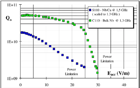
Next figure shows a typical Q0 versus Eacc for niobium thin films onto copper cavities.
Figure 3.8.Example of typical Q vs Eacc at 1,7 K of niobium coating on copper cavities of 1,5GHz [27].
However it is possible to get very good performance by the using of the niobium film technology. The use of film cavities for accelerators operating at 1.7 K was not contemplated because of the supposedly “intrinsic” limitations of films, which could prevent operation at high RF amplitudes with high Q values. Nevertheless, such limitations are experimentally not confirmed. Next figure shows the Q value as a function of the accelerating RF field for some of the best performing cavities studied at CERN in which Q values of 1e10 at 15 MV/m and 4e9 at 20 MV/m were obtained.
26
Figure 3.9 The Q factor versus accelerating field for the best Nb-Sputtered Cu 1,5 GHz cavity fabricated at CERN [28]
In order to understand the Q-drop in thin films, it will be necessary to discuss the Q-drop in niobium bulk cavities.
3.11 Bulk cavity Q-drop
Some years ago, the Q drop was considered as a typical feature of BCP cavities since the KEK group could show that the electro-polishing process did not give significant problems. The Q-drop was named by K. Saito the “European headache”. Few years after, the CEA/ Saclay group discovered that an in-situ bake at moderate temperatures between 90-120°C partially alleviated the Q-drop problem. The same was shown later in the study of electro-polished cavities, which had also shown Q-drop at DESY, a fact that created confusion as to the claimed superiority of electro-polishing. Later, it was understood that a moderate temperature baking was part of the Japanese electro-polishing procedure. It has to be noted, however, that the baking effect is generally more pronounced in electro-polished cavities, i.e. often a small residual Q-drop remains in the chemically electro-polished (BCP) cavities after baking.
But it is necessary to note that Q-drop is not at all unusual. This problem can have many different origins and explanations. A material with a low RRR, for instance, shows higher resistance at low field, stronger Q-slope and earlier onset of Q-drop. The lower the RRR, the stronger the above features. However, there are exceptions to this rule. One example for this was observed in 9.56 GHz cavity that reached a 150 mT peak magnetic field with very little Q-drop, made from a material of RRR ~50. Cavities made from deep drawn polycrystalline sheet material, which haven’t undergone the initial 100 micron etching to remove the “damage layer”, also show strong Q-slope and early onset of Q-drop [49].
Recently Visentin [51] showed that the Q-drop can also be avoided with a heat treatment at 145°C for 3 hours, instead of the established 48 hours at 120°C. It was a significant technological advancement, which allowed shortening of the cavity processing time. Since both, these baking conditions result in the same oxygen profile in the Nb surface, as calculated from a simple diffusion model, this finding also suggests a possible role of oxygen in the Q-drop phenomenon. The role of oxygen was already suspected when measurements indicated that the reduction in BCS resistance that
27
accompanies the baking disappears after removing of ~100 nm of material from the surface. This is consistent with the thermal diffusion length of oxygen at the baking temperature and duration.
The baking effect on the BCS resistance remains after long-term exposure to air and high pressure water rinsing. The baking effect on the BCS resistance saturates after a certain bake-out time. When removing surface layers in a baked cavity in small steps, the BCS resistance slowly rises again. After removal of 300 nm from the surface the BCS resistance of before baking is restored. But recent studies showed that Q-drop re-appears after removal of ~10 nm from the Nb surface through anodization in a baked cavity. This could indicate that the origin of the Q-drop effect is located in an even thinner surface layer. Possibly this could also hint at the change of BCS resistance with baking being just a secondary benefit of the baking, with both effects, BCS resistance change and Q-drop, actually having different origins [51] [53].
Respect to the thin films, Q-slopes in the bulk case have different origins. In Figure 3.10 it is possible to note a softer Q-slope for the bulk cavity at medium accelerating fields and a steeper one above 25 MV/m. Performances of Eacc are in both cases limited by the RF power supply available.
Figure 3.10. Comparison of Q drops between thin films and Nb bulk cavities
The physical reason of the high field Q-slope removal by baking is a challenging issue and many studies have been carried out in order to find an explanation. In parallel, several theories have
28
been pushed forward to explain the Q-slope existence. In order to understand the Q-slope, it is necessary to review the latest results with the secret hope to clear up by the way the thin film issue.
For a bulk cavity, it is necessary to consider three different Q-slopes in the Q0 (Eacc) curve:
at low (LF), medium (MF) and high fields (HF). This slopes can be seen in the next figure.
Figure 3.11 Low, medium and high field Q-slopes
3.11.1. Low Field Q-slope
Halbritter [54] analyzed the topic, saying that the Q-slope at low field is due to the presence of NbOx clusters in niobium, located at the oxide-metal interface, providing localized states inside
the Nb energy gap, therefore increasing the surface resistance. This explanation could help to understand some experimental observations:
• After cavity baking, the low field Q-slope enhancement could be caused by additional clusters due to the interstitial oxygen diffusion.
• After hydrofluoric rinse of the baked cavity, low field Q-slope is restored as before baking. Due to hydrofluoric acid just removes the niobium oxide and that a new oxide layer is later rebuilt at the surface, the low field Q-slope origin is necessarily located in the oxide layer or at the oxide-metal interface as NbOx clusters.
29
By the other hand V. Palmieri [34], says that the low field increase of the Q-factor can be mathematically described by the presence of an overlayer made of a poor superconductor. The low field increase of Q factor can be easily explained by simply calculating the surface impedance of the bilayer system (as is shown in next figure) made of the base superconductor SC2 coated by a thin layer of a poorer superconductor (SC1) of a given thickness a. The penetration depths of the two superconductors are respectively λ2 and λ1. It is necessary to note the experimental evidence that some of the most striking cases of Q-increase at low fields are found in cavities whose internal surface was either specially or contaminated by the presence of over layers.
Figure 3.12. 2 Bilayer system made of the bulk niobium (SC 2 ) and of an over-layer of a superconductor (SC 1) with poorer superconducting properties.
In this model is presented a hypothesis in which being the over-layer a contaminated film, for low field intensities, its penetration depth λ1 can depend on the reduced magnetic field b = B/BC as in the following relation:
𝜆1(𝐵) ≌ 𝜆1(0) + 𝛼 ∗ 𝑏 (3.33)
By only this statement, it can be explained how, at low fields, the Q-factor can increase versus magnetic field. It is also possible to say that, the more λ1 increases with magnetic field, the more the “clean and high performance” SC2 is involved. After some calculations and algebra, the final relation for a bilayer Q factor is the following
30
𝑄𝑇𝑂𝑇 = 𝑄1(0) ∗ (1 − 𝑒(𝜆1−𝛼𝑏−𝑎 )) + 𝑄2 (0) ∗ 𝑒−𝑘2𝑏 ∗ 𝑒(
−𝑎
𝜆1−𝛼𝑏) (3.34)
By previous equation, it can be noted that the role of SC1 is strongly dissipative and that the SC1 related Q-factor is increasing versus field. As far as the second term is concerned instead, by increasing the field, the penetration depth in SC1 becomes higher and the losses are more and more shifted into the SC2 that is a pure superconductor and has lower losses. This mechanism however shows a maximum. Strong fields saturate the SC2, giving rise to normal dissipative fields. The composition of the two terms presents also a maximum at even lower field value. The dependence of the maximum of QTotal versus the thickness a of SC1 can also be observed. At a first sight, the Q rise
versus field can appear as a benefit, but it is easy to observe that for lower values of a, the value of the QTotal at the maximum also increases, proving that actually the presence of the over layer is a
source of losses and it is not beneficial. However the presence of a Q-increase versus field can give useful information about the superficial contamination: the higher is the field at which the maximum occurs, the thicker is the over layer [34].
3.11.2. Medium Field Q-slope
Respect to the Q0 (Eacc) evolution in the medium field range, a linear and a quadratic increases
of the surface resistance RS (∝ 1/Q0) on the peak surface magnetic field B (∝ Eacc) have theoretically
been established .The linear dependence (Equation 7.1) is linked to hysteresis losses due to Josephson fluxons in weak links (oxidation of grain boundaries). As regards quadratic dependence (see Equation 7.2), it is produced by a surface heating due to the thermal impedances of Nb and Nb-He interface.
𝑅𝑆 = 𝑎 + 𝑏 𝐵 (7.1)
𝑅𝑆 = 𝑅0 (1 + 𝛾
𝐵2 𝐵𝑐2)
(7.2)
Here Bc is the thermodynamic critical field of niobium and R0 is the surface resistance at small
magnetic fields [54].
![Figure 3.8.Example of typical Q vs Eacc at 1,7 K of niobium coating on copper cavities of 1,5GHz [27]](https://thumb-eu.123doks.com/thumbv2/123dokorg/4712891.45314/41.892.234.704.209.524/figure-example-typical-eacc-niobium-coating-copper-cavities.webp)
![Figure 3.13 Test result of the single crystal cavity at Jefferson laboratory [57]](https://thumb-eu.123doks.com/thumbv2/123dokorg/4712891.45314/48.892.220.711.702.1046/figure-test-result-single-crystal-cavity-jefferson-laboratory.webp)
![Figure 3.14. Performance limitations regarding the quality factor Q or the accelerating electric field E in the Q vs (E) curve [57]](https://thumb-eu.123doks.com/thumbv2/123dokorg/4712891.45314/49.892.124.768.533.882/figure-performance-limitations-regarding-quality-factor-accelerating-electric.webp)