Scuola Dottorale di Ingegneria
Sezione di Ingegneria dell’Elettronica Biomedica, dell’Elettromagnetismo e delle Telecomunicazioni
Design of Metamaterial-Inspired Electrically Small
Active Radiating Elements
Progettazione di Elementi Radianti Attivi Elettricamente Corti Ispirati ai Metamateriali
Fabrizio Trotta
(XXVII Ciclo della formazione Dottorale)
Abstract
In this thesis, we present the a detailed description of the work and the results achieved on the research for the study of innovative active electromagnetic components and radiating microwave components metamaterial-inspired, which can be easily integrated in practically realizable systems for industrial application .
First, we analyze the use of non-Foster active circuits to obtain a widening of the operating bandwidth of devices based on metamaterials (MTMs); in particular we present study and realization of a demonstrator NIC (Negative Impedance Converter) compact, high integration and low cost, made of printed circuit with discrete components in SMD (Surface Mount Technology). The non-Foster circuit is designed by using only real components and the stability of the entire system is properly evaluated.
Then we explore the possibility to generate an electromagnetic field with a non-zero orbital angular momentum (OAM) using a single patch antenna. In particular, we report an analytical study of a circular patch antenna in order to show that a circular polarized TMnm mode generates an OAM of order n-1. Then, we design an elliptical patch antenna
that radiates a circular polarized electromagnetic field with OAM of the first order. Third, we propose a new class of horn antennas with integrated MTM-inspired filtering modules. In particular, we present some horn antennas that, depending on the used resonant inclusion, show a band-pass or band-stop filtering and polarization transformer behavior.
Afterward, we present some radiating elements based on the use of MTM-inspired resonant inclusions. As an example, we propose a compact antenna for Wi-Fi application consisting of two orthogonal parasitic meandered monopoles and a driven bow-tie.
Finally, we show that properly designed mantle cloaks, consisting of patterned metallic sheets placed around cylindrical monopoles, allow tightly packing the same antennas together in a highly dense telecommunication platform. Our experimental demonstration is applied to the relevant example of two cylindrical monopole radiators operating for 3G and 4G mobile communications.
Acknowledgements
The completion of my dissertation has been a long journey in which many people have scientifically and humanly contributed. In the next few lines, I will try to thank all the people who supported me, without whose help I could not have made this journey.
I want to express my deeply-felt thanks to my supervisor, Prof. Filiberto Bilotti, Head of the Antennas & Special Materials Research Laboratory, who, starting from my B.S. degree, has always tried to bring me on the frontier of metamaterials science. I sincerely thank also Prof. Alessandro Toscano, Head of the Electromagnetic Diagnostic Laboratory, for his warm encouragement and thoughtful guidance during my research activities. They deserve my heartfelt gratitude for giving me the opportunity to enter the world of higher education and research, and for their valuable advice, constructive criticism and extensive discussions around my work.
My gratitude is also extended to all members of the Department of Engineering at “Roma Tre” University, for the excellent and pleasant working environment. I express my special thanks to my friends and colleagues Dr. Mirko Barbuto, Dr. Alessio Monti and Dr. Davide Ramaccia, with whom I have enjoyed many useful and entertaining moments.
I would like to thank Elettronica S.p.A for the use of their near-field measurement system and for support in measurements.
Last but not least, I want to reserve a special word of gratitude to my family, my wife Francesca and my fabulous sons Flavio and Alessio, who have brought great joy to my life. They deserve thanks for their love and a huge variety of other reasons.
Fabrizio Trotta “Roma Tre” University April 2016
Table of Contents
ESTESO SOMMARIO ... 2
INTRODUCTION ... 7
NON-FOSTER ACTIVELY NIC LOADED FOR ELECTRICALLY-SMALL METAMATERIAL BASED-ANTENNAS ... 17
1.1 GENERAL CONSIDERATION OF FREQUENCY BAND CHOSEN FOR THE PROJECT ... 19
1.2 NON-FOSTER TECHNOLOGY ... 22
1.3 TECHNOLOGY SCOUTING FOR NIC SOLUTION ... 23
1.4 IDENTIFICATION OF TECHNOLOGY AND CHOICE OF NIC CIRCUIT SOLUTION ... 24
1.5 IMPLEMENTATION SELECTED NIC CIRCUITAL SOLUTION. ... 27
1.6 NIC MODEL ON ADS CIRCUIT SIMULATOR. ... 29
1.7 PCB DESIGN AND CIRCUIT ROUTING ... 37
1.8 INDUSTRIALIZATION AND MANUFACTURING NIC PROTOTYPES ... 39
1.9 PERFORMANCE MEASUREMENT NIC PROTOTYPES ... 47
1.10 ADDITIONAL EXPERIMENTAL TESTS AND FUTURE RESEARCH ACTIVITIES ... 48
1.11 SUMMARY ... 49
1.12 REFERENCES... 50
CIRCULAR POLARIZED PATCH ANTENNA GENERATING ORBITAL ANGULAR MOMENTUM ... 53
2.1 ANALYTICAL STUDY ... 54
2.2 VALIDATION THROUGH FULL-WAVE NUMERICAL SIMULATIONS ... 59
2.3 EXPERIMENTAL REALIZATION AND MEASUREMENTS ... 63
2.4 SUMMARY ... 64
2.5 REFERENCES... 65
HORN ANTENNAS WITH INTEGRATED MTM-INSPIRED FILTERING MODULES ... 67
3.1 LINEAR-TO-CIRCULAR POLARIZATION TRANSFORMER ... 68
3.2 A COMBINED BAND-PASS FILTER AND POLARIZATION TRANSFORMER FOR HORN ANTENNAS 69 3.2.1 Design of a planar Linear-To-Circular Polarization Transformer ... 69
3.2.2 Design of the Self-Filtering Circularly Polarized Horn Antenna ... 73
3.2.3 Experimental Realization and Measurements ... 76
3.3.1 Design of a Horn Filtenna with a Single-Band-Stop Characteristic ... 78
3.3.2 Design of a Horn Filtenna with a Dual-Band-Stop Characteristic ... 83
3.3.3 Experimental Realization and Measurements ... 86
3.4 SUMMARY ... 88
3.5 REFERENCES ... 90
COMPACT AND MULTI-FUNCTIONAL ANTENNAS BASED ON MTM-INSPIRED STRUCTURES ... 92
4.1 DESIGN OF A COMPACT ANTENNA BY USING ORTHOGONAL PARASITIC MEANDERED MONOPOLES ... 92
4.1.1 Introduction... 92
4.1.2 Antenna Design with Equal Meandered Monopoles ... 94
4.1.3 Antenna Design with Slightly Different Meandered Monopoles ... 97
4.2 SUMMARY ... 101
4.3 REFERENCES ... 101
MANTLE CLOAKING FOR CO-SITE RADIO-FREQUENCY ANTENNAS ... 104
5.1 DESIGN MANTEL CLOAKS ... 105
5.2 SIMULATION AND EXPERIMENTAL RESULTS ... 107
5.3 SUMMARY ... 112
5.4 REFERENCES ... 113
PUBLICATIONS ... 115
BIOGRAPHICAL NOTE ... 117
APPENDIX 1 ... 118
1. VERIFICHE SPERIMENTALI AGGIUNTIVE SUI NIC PROTOTIPALI ... 118
2. FINALIZZAZIONE DI UN EFFICACE ED EFFICIENTE MODELLO SIMULATIVO FULL-WAVE NON LINEARE 123 3. VARIANTI PREVISTE SUL PCB PER ESSERE SVILUPPATO SU SINGOLO STRATO ... 124
4. ANALISI DI POSSIBILI SOLUZIONI CIRCUITALI NIC ALTERNATIVE ED EVENTUALE REALIZZAZIONE ... 126
List of Figures
Fig. 1: Radio spectrum for modern broadcast communications technologies. ... 19
Fig. 2: Reactance behavior of Foster and Non-Foster networks type ... 22
Fig. 3: Equivalent circuit of an ideal electrically short dipole... 23
Fig. 4: Linvill circuit for the NIC device. ... 24
Fig. 5: Linvill SCS circuit in Short Circuit Stable configuration. ... 25
Fig. 6: Input impedance of the NIC quadrupole model ... 26
Fig. 7: NICs Open and Short Circuit Stable configuration... 26
Fig. 8: NIC Stability Condictions ... 26
Fig. 9: Packaging and description of BJT ... 28
Fig. 10: S2P linear model of the active two-port BJT device... 29
Fig. 11: Results obtained from linear model S2P active two-port device with ADS ... 30
Fig. 12: DS BFG520: S-Parameters ... 30
Fig. 13: BJT SPICE Model with Packaging ... 31
Fig. 14: Equivalent Circuit BFG520: SPICE Parameters+ package SOT343N ... 32
Fig. 15: Non-linear three ports transistor ADS model with DC bias ... 33
Fig. 16: Results obtained with the non-linear model @ Vce = 6 V Ic = 20.6 mA ... 33
Fig. 17: Frequency behavior performance of NCI/NII device ... 34
Fig. 18: ADS NCI model ... 34
Fig. 19 Return loss of the NIC model in NCI configuration ... 35
Fig. 20 Electrical Scheme drawing of the PCB NCI solution ... 36
Fig. 21 NIC PCB Model Prototype Solution ... 37
Fig. 22 CST CAD Model for Prototype Solution ... 38
Fig. 23: S11 Simulation results PCB NCI model: CST MWS Vs ADS ... 38
Fig. 24: NIC circuit diagram including choke for isolation network in DC. ... 40
Fig. 25: Choke circuit diagram for the isolation in DC and the RF signal attenuation.41 Fig. 26: ADS circuit model with the biasing and isolation network ... 42
Fig. 27: ADS Simulation results: Broadband S11 impedance and DC absorption ... 42
Fig. 28: ADS Simulation results: Broadband S11 input impedance with a better Q factor ... 43
Fig. 29: ADS Circuit model for the unconditional stability analysis ... 44
Fig. 30: Simulation of the unconditional stability factor for the active device. ... 44
Fig. 31: Industrialized NIC PCB solution for experimental testing ... 45
Fig. 32: Critical via holes on the chosen PCB solution. ... 46
Fig. 33: NIC prototype SN01. ... 46
Fig. 34: NIC prototype SN02. ... 47
Fig. 35: NIC prototype SN02. ... 47
Fig. 36: Broadband characterization of prototypes: S11 Vs Frequency ... 48
Fig. 37: Geometrical sketch of a circular patch antenna. The main geometrical parameters are the radius of the patch a and the thickness of the dielectric substrate h. 55 Fig. 38: Ratio between the amplitude of the terms A and B in the case of a circular patch antenna working in a CP TM21 mode for different values of substrate permittivity. ... 57
Fig. 39: Phase patterns (in degree) of the x (left) and y (right) component of the radiated electric field in the case of: (a) RHCP TM11 mode; (b) RHCP TM21 mode; (c) RHCP TM31 mode. ... 59
Fig. 40: Top view of the elliptical patch antenna. The inner conductor of the coaxial cable is connected to the point p (x = 8.75 mm; y = 21 mm). The origin of the reference system is at the shape centre. Antenna dimensions are: A1 = 75,2 mm, A2 = 81.6 mm, and L = 100 mm. ... 60
Fig. 41: Simulated (red-solid line) and measured (black-dashed line) reflection coefficient amplitude of the proposed elliptical patch antenna shown in Fig. 93... 61
Fig. 42: Phase patterns at 2.4 GHz of the x (left) and y (right) component of the radiated E field by the elliptical patch antenna working in a RHCP TM21 mode... 62
Fig. 43: Simulated Azimuth (left) and Elevation (right) radiation phase patterns at 2.4 GHz of the elliptical patch antenna, shown in Fig. 93, working in a RHCP TM21 mode. ... 62
Fig. 44: 3-D directivity pattern at 2.4 GHz of the antenna shown in Fig. 93. ... 62 Fig. 45: Photograph showing the realized elliptical patch antenna with the dimensions given in Fig. 93. ... 63
Fig. 46: Measured Azimuth (left) and Elevation (right) radiation phase patterns at 2.4 GHz of the prototype shown in Fig. 98. ... 64
Fig. 47: Geometrical sketch of the proposed polarization transformer with dimensions: L = 5.8 mm, La1 = 0.3 mm, La2 = 0.9 mm, Lm = 0.8 mm, Wd = 0.4 mm, Wa = 0.4 mm. 70
Fig. 48: Geometrical sketch of the proposed polarization transformer and its integration with a linearly polarized rectangular waveguide. ... 71
Fig. 49: Reflection coefficient amplitude of an open ended rectangular waveguide (dashed line) and of the structure shown in Fig. 44 (solid line). ... 72
Fig. 50: Realized gain patterns at 15.75 GHz of the structure shown in Fig. 44: (left) φ = 0°; (right) φ = 90°. ... 72
Fig. 51: Axial ratio for the main beam direction of the structure shown in Fig. 44. .... 73 Fig. 52: Side view (left) and perspective view (right) of the filtering circularly polarized horn antenna. Corrugated horn dimensions: Ds = 6.3 mm, Lg = 33 mm, Lh = 25.6 mm, Lt
= 5 mm, Ws = 1.3 mm, Wr = 1.3 mm. ... 74
Fig. 53: Simulated and measured reflection coefficient amplitude of the self-filtering circularly polarized horn antenna shown in Fig. 48. ... 75
Fig. 54: Simulated and measured axial ratio for the main beam direction of the self-filtering circularly polarized horn antenna shown in Fig. 48. ... 75 Fig. 55: Simulated and measured realized gain patterns at 15.85 GHz of the self-filtering circularly polarized horn antenna shown in Fig. 48: (left) φ = 0°; (right) φ = 90°. ... 76
Fig. 56: Realized gain (solid line) and directivity (dashed line) of the self-filtering circularly polarized horn antenna shown in Fig. 48. ... 76
Fig. 57: Photographs showing: (a) side view of the overall antenna structure consisting of a coaxial-to-waveguide transition, the proposed polarization transformer, and a corrugated conical horn; (b) front view of the overall antenna structure; (c) the realized polarization transformer; (d) the overall antenna structure in the Satimo StarLab. ... 77
Fig. 58: Geometrical sketch of the proposed horn antenna with the notched-band filter: (a) perspective view; (b) front view; (c) side view. ... 79
Fig. 59: Reflection coefficient amplitude at the input port of the structure shown in Fig. 54 for different positions of the SRR. ... 80
Fig. 60: Measured and simulated reflection coefficient amplitude at the input port of the structure shown in Fig. 54 for the case of d = 15 mm. ... 81
Fig. 61: Measured and simulated realized gain in the main beam direction of the proposed horn antenna with the notched-band filter and of the corresponding standard horn antenna. ... 82
Fig. 62: Close-up of Fig. 57. ... 82 Fig. 63: Simulated and measured realized gain patterns of the proposed horn antenna with and without the notched-band filter on the E-plane (left column) and H-plane (right column) at: (first line) 9 GHz, (second line) 10 GHz and (third line) 11 GHz. ... 83
Fig. 64: Geometrical sketch of the proposed horn antenna with the dual-band-notch filter: (a) perspective view; (b) front view; (c) side view. ... 84
Fig. 65: Simulated and measured reflection coefficient amplitude at the input port of the horn filtenna with a dual band-stop characteristic. ... 85
Fig. 66: Simulated realized gain in the main beam direction of the horn antenna with and without a dual-band-stop filter. ... 85
Fig. 67: Close-up of the simulated realized gain in the main beam direction of the horn antenna with and without a dual-band-stop filter. ... 86
Fig. 68: Photographs showing: top (a) and bottom (b) views of the realized filtering module; (c) the filtering module fixed in the horn antenna; (d) perspective view of the proposed self-filtering horn antenna; (e) the proposed structure placed inside the near-filed measurement system. ... 87 Fig. 69: Photographs showing the transmission measurement setup. ... 88 Fig. 70: Power transmission between two single-band filtering horn antennas, two standard horns and between a standard horn and the single-band filtering horn antenna, in the setup shown in Fig. 65. ... 88
Fig. 71: Perspective view of the proposed antenna. The ground side is 10 cm. ... 94 Fig. 72: Front view (a) and back view (b) of the proposed antenna with equal meandered monopoles. Antenna dimensions are: RBT = 4.9 mm, Hm = 4.5 mm, gm = 0.3 mm, wm =
0.48 mm, L = 3 mm. ... 95 Fig. 73: Reflection coefficient amplitude of the proposed antenna with equal meandered monopoles. ... 96
Fig. 74: Realized gain pattern at the resonant frequency (2.425 GHz) of the antenna with equal meandered monopoles. ... 96
Fig. 75: Surface currents on the two meandered monopoles at the resonant frequency of the overall structure (2.425 GHz). ... 97
Fig. 76: Front view (a) and back view (b) of the proposed antenna with slightly different meandered monopoles. Antenna dimensions are: RBT = 5 mm, Hm = 4.5 mm, gm = 0.3
mm, wm = 0.48 mm, L = 3 mm. ... 98
Fig. 77: Reflection coefficient amplitude of the proposed antenna with slightly different monopoles (red-solid line), compared to the one of the previous case (black-dashed line). ... 99 Fig. 78: Surface currents on the two meandered monopoles at the lowest resonant frequency of the overall structure shown in Fig. 25. ... 99
Fig. 79: Surface currents on the two meandered monopoles at the highest resonant frequency of the overall structure shown in Fig. 25. ... 100
Fig. 80: Realized gain pattern at the lowest resonant frequency (2.416 GHz) of the antenna with slightly different monopoles. ... 100
Fig. 81: Realized gain pattern at the highest resonant frequency (2.461 GHz) of the antenna with slightly different monopoles. ... 101
Fig. 82: Photograph of the fabricated system, consisting of two electrically ... 106 Fig. 83: . SCS of the uncloaked (continuous line) and cloaked (dashed line) LTE antenna for a plane wave excitation. In the insets, it is possible to appreciate the 3D bistatic scattering cross section of the antenna in the uncloaked (left) and cloaked (right) case. The scale used for the two scattering patterns is the same ... 108
Fig. 84: (a)-(c) Magnitude of the reflection coefficient at the input ports of the monopoles shown in Figure 82 in the isolated, uncloaked, and cloaked scenarios, respectively. (d) Mutual coupling between the two monopoles in the uncloaked and cloaked scenarios. The horizontal line represents the commonly used matching threshold at - 10 dB. ... 109
Fig. 85: (a) Far-field measured realized gain patterns of the UMTS monopole at three frequencies around the cloaking frequency in the isolated, uncloaked, and cloaked cases; (b) Schematic view of the three considered scenarios (isolated, uncloaked, and cloaked). ... 110 Fig. 86: Snapshot in time of the transverse electric field distribution on a plane perpendicular to the monopole axes at the two boundary frequencies in the isolated, uncloaked, and cloaked case. The blue circles show the position of the two monopole ... 111
List of Tables
Table 1: Bill Of Material of PCB NIC in NCI configuration ... 36 Table 2: Bill Of Material of PCB NIC in NCI configuration ... 37
Esteso Sommario
(Italiano)
l termime “metamateriale” (MTM) è nesso ad un esteso insieme di materiali sintetici, sintetizzati, introducendo ad esempio delle strutture metalliche di particolare forma e dimensione all’interno di un mezzo dielettrico ospitante [1]-[4]. I parametri costituzionali di tali inclusioni sono progettati per modificare la risposta del materiale ospitante ed ottenere proprietà inconsuete non riscontrabili nei materiali convenzionali alle frequenze di interesse. Benché alcuni materiali naturali mostrano su alcune bande di frequenza dello spettro elettromagnetico (infrarosso, visibile e ultravioletto [5]-[6]), valori anomali negativi o nulli della permittività elettrica, alle frequenze delle microonde non sono noti in natura materiali con caratteristiche simili. Anche le proprietà magnetiche dei materiali naturali sono limitate alle frequenze radio ed alle basse microonde [7] e valori anomali di permeabilità magnetica non sono naturalmente disponibili nel dominio visibile, infrarosso e ultravioletto. Tuttavia, quando la natura non ci fornisce i valori necessari dei parametri elettromagnetici, i MTM possono essere utilizzati con successo per ottenere i valori anomali desiderati.
Ad esempio, come anticipato teoricamente in [8] e dimostrato sperimentalmente in [9], è possibile ottenere un MTM caratterizzato da un indice di rifrazione negativo alle frequenze delle microonde combinando opportunamente sottili fili metallici [10] e split-ring resonator (SRR). Infatti, poiché in tale materiale le inclusioni e la distanza tra di esse sono inferiori rispetto alla lunghezza d’onda operativa, è possibile introdurre valori efficaci di permettività, permeabilità e indice di rifrazione, i quali possono assumere valori anomali. La loro sintesi prende spunto dall’idea introdotta da Pendry [9], secondo la quale una serie di dipoli elettrici orientati causa un comportamento risonante della permittività elettrica efficace del mezzo. In modo simile, un insieme di dipoli magnetici genera un’analoga risonanza della permeabilità magnetica efficace associata al MTM. Se le due risonanze si verificano nello stesso intervallo di frequenze, siamo in grado di
I
sintetizzare un materiale con un indice di rifrazione negativo in un determinato intervallo di frequenze.
L’elemento fondamentale per la realizzazione del primo MTM è stato quindi lo SRR, il quale è un risonatore miniaturizzato utile per ottenere il magnetismo artificiale alle frequenze delle microonde. Un singolo SRR è costituito da due anelli aperti concentrici di materiale metallico, le cui aperture sono poste a lati opposti della struttura. Tale configurazione permette di aumentare la capacità totale del risonatore rispetto a quella di una struttura a singolo anello, aggiungendo una capacità distribuita tra i due anelli concentrici. In questo modo, la frequenza di risonanza del risonatore può essere significativamente ridotta per raggiungere una dimensione elettrica dell’ordine di λ/10. Dopo quanto proposto in [9], sono state introdotte molte inclusioni magnetiche differenti per ottenere un maggiore grado di miniaturizzazione, rimuovere la bi-anisotropia intrinseca che caratterizza il comportamento di uno SRR [11]-[14], e ottenere una risposta isotropa [15]-[18].
Accanto a questi sforzi modellistici, sono state investigate molte proprietà innovative dei MTM. In particolare, l’effetto di super-risoluzione di un MTM con indice di rifrazione negativo ha mostrato come sia possibile superare il limite fisico della diffrazione. Una lente convenzionale, infatti, è in grado di focalizzare un dettaglio con un limite ben noto in ottica: fissata la frequenza operativa, tale dettaglio non può essere inferiore alla corrispondente lunghezza d’onda di lavoro. Una lamina opportunamente progettata di MTM può invece andare idealmente al di sotto del limite fisico della diffrazione, focalizzando dettagli con dimensioni inferiori alla lunghezza d’onda. Altre applicazioni interessanti dei MTM derivano dall’idea che, se utilizziamo insieme una coppia di materiali artificiali coniugati, possiamo progettare cavità risonanti di dimensioni trasversali molto inferiori alla lunghezza d’onda. A partire da questa idea di base, sono stati proposti numerosi componenti e dispositivi innovativi basati sulle propietà dei MTM, come ad esempio super-lenti [19]-[20], iper-lenti [21], rivestimenti per l’invisibilità elettromagentica [22]-[24], componenti radianti compatti [25]-[29], dispositivi per l’aumento della trasmissione da foro elettricamente piccolo [30]-[36], filtri [37], assorbitori [38], ecc. Inoltre, negli ultimi anni, sfruttando le potenzialità offerte dalla nano-fabricazione, il range operativo in frequenza dei MTM è stato esteso fino alle
frequenze ottiche [39]-[43]. In questo caso, tuttavia, i risonatori magnetici usati alle microonde non possono essere facilmente impiegati [44] e, di conseguenza, sono stati introdotti design alternativi con un minore grado di miniaturizzazione [45]-[46], o basati su approcci concettualmente differenti [47]-[48].
Tuttavia, qualunque sia la gamma di frequenze di interesse, i materiali magnetici artificiali o più in generale i MTM presentano alcune limitazioni intrinseche. A causa di considerazioni energetiche, infatti, ogni MTM passivo deve essere necessariamente un mezzo dispersivo [49]. I valori desiderati dei parametri elettromagnetici sono quindi ottenuti soltanto in un ristretto intervallo di frequenze e, di conseguenza, la banda operativa dei componenti basati su MTM è tipicamente a sua volta limitata. Inoltre, come risulta chiaro dalle relazioni di causalità di Kramers-Kronig, il fenomeno di dispersione è sempre legato a meccanismi di perdita [49], i quali riducono ulteriormente le potenzialità dei MTM.
Per ovviare all’inconveniente della limitazione in banda, alcuni lavori allo stato dell’arte hanno suggerito che, nella costruzione della cella elementare costituente il MTM, sia inserito un elemento attivo che possa aumentare la banda, compensando i fenomeni di risonanza associati al MTM. Questo può essere realizzato abbastanza facilmente nel dominio delle frequenze RF mentre è assai difficile per frequenze più alte.
Nella tecnica dei sistemi riceventi, la tecnologia non-Foster Matching ha la capacità di raggiungere maggiori larghezze di banda istantanea e/o adattamento d’impedenza mediante l’utilizzo di dispositivi Negative Impedance Converter (NIC). Quest’ultimi sono particolari dispositivi attivi elettronici in grado di comportarsi come carichi negativi che iniettano energia nei circuiti, a differenza dei carichi ordinari che la dissipano.
Il vantaggio ottenibile utilizzando la tecnologia non-Foster congiunta a quella metamaterial-based sull’elemento radiante, può allo stato dell’arte svolgere un ruolo strategico fondamentale nella ricerca della soluzione più adatta, innovativa e prestazionale nel campo della progettazione di dispositivi radianti attivi a larga banda ispirati ai MTM.
Il Capitolo 1 di questa tesi è, quindi, dedicato all’impiego di elementi attivi NIC per applicazioni Non-Foster impedance Matching su Electrically small metamaterial-based
antennas per applicazioni UWB in banda VHF/UHF. Innanzitutto, partendo da una breve descrizione teorica della tecnologia Non-Foster, determineremo la tipologia circuitale del carico attivo richiesta per compensare la reattanza intrinseca dell’elemento elettricamente corto ed ottenere un adattamento di impedenza a banda larga mediante un dispositivo NIC. Verrà poi presentato il lavoro di scouting tecnologico che, associato all’analisi di alcuni lavori sperimentali, ci consentirà di individuare la soluzione circuitale e tecnologica prescelta per il progetto del NIC a componenti discreti. E’ stata quindi riportata la ricerca sulla componentistica attiva e passiva necessaria all'implementazione della soluzione circuitale prescelta. In particolare, partendo dai DS forniti dai principali fornitori, sono stati individuati i componenti passivi e attivi a basso costo disponibili sul mercato per applicazioni di tipo civile. Con il simulatore circuitale ADS è stata compiuta un’analisi qualitativa delle componenti circuitali parassitiche dei elementi attivi; l’analisi ha permesso di definire lo schema elettrico del NIC con i valori nominali dei componenti SMD selezionati. Lo schema è stato successivamente implementato nel modello circuitale sul simulatore ADS e tramite questo sono state effettuate le simulazioni per la verifica di fattibilità del dispositivo. Per un’analisi quantitativa delle componenti circuitali parassitiche è stato realizzato un modello 3D mediante il simulatore CST MWS.
Il Capitolo 2 di questa tesi sarà invece dedicato ad una particolare manipolazione che
può essere eseguita su un segnale elettromagnetico ovvero la generazione del momento angolare orbitale (OAM). In particolare, la recente estensione del concetto di OAM dalle frequenze ottiche a quelle delle microonde ha portato alcuni ricercatori ad esplorare come le tecniche radiative a microonde possano essere utilizzate per irradiare un campo elettromagnetico con OAM non nullo. A tal riguardo, il lavoro svolto mira a presentare un nuovo approccio per generare un campo con OAM non nullo attraverso l’utilizzo di una singola antenna a patch. Utilizzando il modello a cavità, per prima cosa analizzeremo il campo irradiato da un patch circolare standard e mostreremo che un modo TMnm a
polarizzazione circolare eccitato mediante due cavi coassiali è in grado di generare un campo elettromagnetico con OAM di ordine ±(n-1). Successivamente, al fine di ottenere una struttura più semplice con un singolo feed, progetteremo un’antenna a patch ellittico in grado di irradiare un modo TM21 a polarizzazione circolare destra. Utilizzando
l’antenna proposta è in grado di irradiare efficacemente un campo elettromagnetico con un OAM del primo ordine.
Nel Capitolo 3, focalizzeremo invece la nostra attenzione sul progetto di antenne ad horn con moduli filtranti integrati ispirati ai MTM. A tale scopo, proporremo l’utilizzo di un trasformatore di polarizzazione realizzato mediante una struttura laminare integrata in guida d’onda. La lamina metallica circolare realizza un trasformatore di polarizzazione costituito da un risonatore complementare elettricamente piccolo intagliato su uno schermo metallico. Mostreremo prima che tale componente è in grado di trasformare la polarizzazione lineare di una guida d’onda rettangolare operante nel suo modo fondamentale in una circolare. Successivamente, integrando tale convertitore di polarizzazione in un horn conico, mostreremo come sia possibile ottenere un’antenna ad horn filtrante in polarizzazione circolare. Il comportamento della struttura proposta sarà validato tramite simulazioni numeriche e misurazioni effettuate su un prototipo.
Si noti, tuttavia, che tale approccio prevede l’inserimento di uno schermo metallico ortogonale alla direzione di propagazione del campo elettromagnetico; di conseguenza, esso può essere utilizzato soltanto per componenti a microonde che debbano mostrare un comportamento di tipo passa-banda. Al fine di progettare antenne ad horn filtranti o componenti a microonde con una carratteristica di tipo notch (elimina banda), dobbiamo quindi rimuovere lo schermo metallico e progettare un’inclusione risonante che sia in grado di immagazzinare/dissipare energia ad una data frequenza, ottenendo così una banda proibita in uno stretto intervallo di frequenze. A tale scopo, presenteremo quindi il progetto di antenne ad horn filtranti con un comportamento elemina banda ottenuto attraverso l’utilizzo di risonatori magnetici elettricamente piccoli. In particolare, uno SRR realizzato su un substrato dielettrico Rogers DuroidTM RT5870 sarà inserito all’interno di un’antenna ad horn ad una opportuna distanza dalla sua apertura. Intorno alla frequenza di risonanza dello SRR la trasmissione sarà quindi fortemente ridotta ottenendo così un comportamento di tipo notch. Al fine di estendere tale risultato al caso di operatività dual-band, proporremo inoltre il progetto di un modulo filtrante costituito da due SRR con dimensioni differenti. Anche in questo caso, la validità dell’approccio proposto sarà verificata attraverso un opportuno set di simulazioni full-wave e esperimenti condotti su prototipi.
Il Capitolo 4 di questa tesi sarà invece dedicato al progetto di nuovi elementi radianti
compatti e multifunzione ispirati ai concetti dei MTM. Presenteremo un’antenna compatta costituita da due monopoli a meandro ortogonali che agiscono come elementi parassiti di un bow-tie alimentato. In particolare, mostreremo che utilizzando due monopoli con dimensioni leggermente differenti è possibile ottenere una maggiore larghezza di banda di impedenza. Utilizzando tale approccio, presenteremo un’antenna compatta operante nella banda del Wi-Fi a 2.4 GHz con dimensioni elettriche complessive pari a
λ
0/ 6
×
λ
0/12
×
λ
0/ 75
.Infine nel Capitolo 5 mostreremo come sia possibile progettare e realizzare, con delle semplici lastre metalliche, mantelli cilindrici su dei monopoli cilindrici in grado di rendere invisibili i monopoli alla radiazione elettromagnetica su piattaforme di telecomunicazioni ad alta densità (tipo stazioni di antenne per cellulari o sulle navi). In queste applicazioni molte antenne operano a breve distanza, diminuendo l’efficienza dell’insieme. Avvolgendo queste antenne con il meta-materiale, si possono isolare EM diventano invisibili una all’altra. In questo modo è stato possibile rendere invisibile un’antenna a banda limitata a vantaggio di un’altra antenna che opera su differenti frequenze. La dimostrazione sperimentale verrà applicata all'esempio pertinente di due radiatori monopoli cilindrici operativi per comunicazioni mobili su standard 3G e 4G
Introduction
he term “metamaterial” (MTM) refers to the wide range of artificially engineered materials, typically synthesized by arranging conductive structures of particular shape and size in a host dielectric medium [1]-[4]. The electromagnetic parameters and geometry of such inclusions are designed to change the response of the host material and obtain special properties that are not achievable by conventional materials at the frequencies of interest. Just to cite an example, though some natural materials (e.g. noble metals and some semiconductors) exhibit unconventional values (i.e. negative or near zero) of the electric permittivity at IR, visible, and UV frequencies [5]-[6], a natural
T
material with similar characteristics in the microwave regime was not known. In the same way, magnetism of natural materials is limited to radio and low-microwave frequencies [7] and, consequently, anomalous permeability values are not naturally available in the IR, visible, and UV domains. When nature does not provide us with the needed values of the material parameters, MTMs can be successfully used to obtain such anomalous values.
For instance, as anticipated in [8] and experimentally demonstrated in [9], it is possible to obtain a MTM characterized by a negative index of refraction at microwave frequencies combining metal thin wires [10] and split-ring resonators (SRRs). In fact, since in such material the inclusions and the distance between them are reduced in size when compared with the operating wavelength, it is possible to introduce effective permittivity, permeability and refractive index of the medium, which can assume anomalous values. Its synthesis starts from the idea introduced by Pendry [9], that a series of electric dipoles properly oriented causes a resonant behavior for the effective electrical permittivity of the medium. Similarly, a set of magnetic dipoles causes a similar resonance of the effective magnetic permeability associated with the MTM. If the two resonances occur at the same frequency range, we are able to synthesize a material with negative refractive index in a specific frequency range.
The key element to the realization of the first MTM was then the SRR, which is a miniaturized resonator useful to obtain artificial magnetism at microwave frequencies. A single SRR consists of two concentric metallic broken rings with the two gaps placed at the opposite sides of the structure. This ingenious design permits to increase the overall capacitance of the resonator with respect to a single ring structure, by adding a distributed capacitance between the two concentric rings. In this way, the resonant frequency can be significantly lowered to reach an electrical size of the order of λ/10. After the work [9], several different magnetic inclusions have been introduced to achieve a higher degree of miniaturization, remove the inherent bi-anisotropy characterizing the electromagnetic behavior of the SRR [11]-[14], and obtain an isotropic response [15]-[18].
Besides these modeling efforts, several innovative properties of MTMs have been investigated. In particular, the effect of super-resolution of a MTM with a negative index of refraction has shown how one can overcome the physical limit of diffraction. A conventional lens, in fact, is able to focus on a detail with a well-known limit in optics:
fixed the working frequency, this detail can not be less than the corresponding operating wavelength. A flat plate of properly designed MTM can instead ideally go below the physical limit of diffraction, focusing details with dimensions smaller than the wavelength. Other interesting applications of MTMs result from the idea that, if we couple together a pairs of conjugated artificial materials, we can design resonant cavities of transverse dimensions much smaller than the wavelength. Starting from these ideas, several innovative components and devices based on MTMs properties have been proposed, such as super-lenses [19]-[20], hyper-lenses [21], cloaking covers [22]-[24], compact radiating components [25]-[29], enhanced transmission devices [30]-[36], filters [37], absorbers [38], etc. Moreover, in the last years, exploiting the potentials offered by nano-fabrication, the operation frequency range of MTMs has been extended up to optical frequencies [39]-[43]. In this case, however, the magnetic resonators used at microwave frequencies cannot be straightforwardly applied [44], and alternative designs with a lower rate of miniaturization [45]-[46], or based on conceptually different approaches [47]-[48] have been introduced.
Whatever the frequency range of interest is, however, artificial magnetic materials exhibit some intrinsic limitations. Due to energy considerations, in fact, any passive MTM is necessarily a dispersive medium [49], meaning that the desired values of the electromagnetic parameters are typically reached only in a narrow frequency range and, consequently, the operation bandwidth of MTM-based components is limited. Moreover, as it is clear from Kramers-Kronig causality relationships, the dispersion phenomenon is always related to loss mechanisms [49] that further reduce the potentials of the designed MTMs.
To get around this problem, some state of art works have suggested that, in the unit cell constituting the MTM, is inserted an active element that can increase the bandwidth, offsetting the resonance phenomena associated with MTM. This can be easily realized in the domain of RF frequencies band, while it is very difficult for higher frequencies
In the technique of receiving systems, the non-Foster Matching technology has the ability to achieve higher instantaneous bandwidths and / or impedance matching using Negative Impedance Converter (NIC) devices. NIC are particular active electronic
devices able to behave as negative loads that inject energy in the circuits, unlike ordinary loads that dissipate.
The advantage achieved by using the non-Foster technology with that metamaterial-based radiating element, can play a key strategic role in the search for the most innovative and high-performance solution in the design of wideband active radiating element devices MTM-inspired.
Chapter 1 of this thesis is, thus, dedicated to the investigation on the use NIC active
element for Non-Foster impedance UWB Matching of Electrically small metamaterial-based antenna application (VHF/UHF band). First, we starting from a short theoretical description of non-Foster technology and we will determine the type of the active load required to compensate the reactance (capacitive) of electrically small radiating element, with the aim of obtaining a broadband impedance matching by means of a NIC device. We will present the work of NIC technology scouting, associated to the analysis of some experimental works, which will allow us to identify the circuit and technology solution for the discrete components NIC project. It 'was then reported research on active and passive circuit components necessary to the implementation of the chosen solution. In particular, starting from Datasheet provided by the suppliers, the passive and active low cost components have identified. Through the ADS circuit simulators, we performed a qualitative parasitic components elements analysis of the active circuit; the analysis allowed defining NIC circuit diagram solution with the nominal values of the selected SMD components. The circuit diagram has been implemented in ADS model and simulations carried out to verify the device feasibility. For a quantitative analysis of circuit components parasites, a full wave 3D model with CST MWS simulator has been created.
Chapter 2 of this thesis will be instead to another possible manipulation that may be
performed on an electromagnetic signal is the generation of orbital angular momentum (OAM). In particular, the recent extension of the OAM concept from optical to microwave frequencies has led some researchers to explore how well established antenna techniques can be used to radiate a non-zero OAM electromagnetic field. In this frame, this chapter is aimed to present a new approach to generate a non-zero OAM field through a single patch antenna. Using the cavity model, we first analyze the radiated field by a standard circular
patch and show that a circular polarized (CP) TMnm mode excited by using two coaxial
cables generates an electromagnetic field with an OAM of order ±(n-1). Then, in order to obtain a simpler structure with a single feed, we design an elliptical patch antenna working on the right-handed CP TM21 mode. Using full-wave simulations and experiments on a
fabricated prototype, we show that the proposed antenna effectively radiates an electromagnetic field with a first order OAM. Such results prove that properly designed patch antennas can be used as compact and low-cost generators of electromagnetic fields carrying OAM.
In Chapter 3, we focus our attention on the design of horn antennas with integrated MTM-inspired filtering module. We propose the use of a polarization transformer achieved through integrated laminar structure in the waveguide. The circular metal foil, realizes a polarization transformer constituted by an electrically small complementary resonator impressed on a metal screen. We will show that this first component is able to transform the linear polarization of a rectangular waveguide (operating in its fundamental mode) in a circular polarization. Then, integrating this polarization transformer in a conical horn, we show how it is possible to obtain a circularly polarized filtering horn antenna (horn filtenna). However, this setup is not planar, consists of different and geometrically orthogonal structures, involves the use of dielectric materials leading to an efficiency reduction, and can handle only low-power signals (i.e. the operation is limited to the receiving mode only). In order to overcome these issues, we then propose a new linear-to-circular polarization transformer that consists of a complementary electrically small resonator etched on a metallic screen. We first show that this component is able to transform the linear polarization of a regular rectangular waveguide working on the fundamental mode into a circular one. Then, integrating this polarization transformer in a conical horn, we show how it is possible to obtain a filtering horn antenna working for circularly polarized signals. The numerical simulations and the measurements performed on a prototype prove the effectiveness of the proposed structure.
Please note, however, that this approach involves the insertion of a metallic screen orthogonal to the propagation direction of the electromagnetic field; therefore, it can be used only for microwave components exhibiting a band-pass behavior. In order to design horn filtennas or microwave components with band-stop characteristic, thus, we need to
remove the metallic screen and design a proper resonant inclusion that stores/dissipates energy at a given frequency, leading to a band-notch in a narrow frequency range. For this purpose, we then present the design of filtering horn antennas with band-stop characteristics obtained through the use of electrically small magnetic resonators. In particular, a SRR etched on a Rogers DuroidTM RT5870 dielectric substrate is inserted within the metallic flare of the horn at a proper distance from the throat. At around the resonant frequency of the SRR transmission is highly reduced and a single notched-band is obtained. In order to extend the result to dual-band operation, we also present the design of the filtering module made by two SRRs with different dimensions. The validity of the proposed approach is verified through proper sets of full-wave simulations and experiments on fabricated prototypes.
Chapter 4 of this thesis will be dedicated to the project of new compact radiating
elements and multifunction inspired by the concepts of the MTM. We will present a compact antenna consisting of two orthogonal meandered monopoles that act as parasitic elements of a driven bow-tie. In particular, we show that by using two monopoles with slightly different dimensions, a greater impedance bandwidth can be obtained. Using this approach, we present a compact antenna operating in the 2.4 GHz Wi-Fi band with overall dimensions of
λ
0/ 6
×
λ
0/12
×
λ
0/ 75
.Finally, in Chapter 5 show how it is possible to design and implement, with the simple metal plates, cylindrical mantle on cylindrical monopoles able to make invisible the monopoles to electromagnetic radiation (on telecommunications stations platforms with high density antennas for mobile devices or on ships )
For these applications, many antennas operate at a short distance, decreasing the efficiency of the radiating element. Load the external surface of these antennas with the MTM cover, it is possible to isolate each other. In this way it was possible to make invisible one antenna to the benefit of another antenna that operates on different frequencies. The experimental demonstration will be applied to the example of two cylindrical monopole antennas for mobile communications on 3G and 4G standards
References
[1] G.V. Eleftheriades, and K.G. Balmain, Negative Refraction Metamaterials: Fundamental Principles and Applications. Hoboken, NJ: Wiley-IEEE Press, 2005. [2] N. Engheta, and R.W. Ziolkowski, Electromagnetic Metamaterials: Physics and
Engineering Explorations. Hoboken, NJ: Wiley-IEEE Press, 2006.
[3] R. Marqués, F. Martín, M. Sorolla, and F. Capolino, Metamaterials with Negative Parameters: Theory, Design and Microwave Applications. Hoboken, NJ: Wiley-Interscience, 2008.
[4] S. Zouhdi, A. Sihvola, and A. P. Vinogradov, Metamaterials and Plasmonics: Fundamentals, Modelling, Applications. Dordrecht, NL: Springer-Verlag GmbH, 2008.
[5] P.B. Johnson, R. W. Christy, “Optical constants of the noble metals,” Phys. Rev. B, Vol. 6, pp. 4370-4379, 1972.
[6] E.D. Palik, Handbook of Optical Constants of Solids, Boston, NE: Academic Press, 1998.
[7] L.D. Landau, L.P. Pitaevskii, and E.M. Lifshitz, Electrodynamics of Continuous Media, Second Edition: Volume 8. Oxford, EN: Pergamon Press, 1984.
[8] V.G. Veselago, “The electrodynamics of substances with simultaneously negative values of ε and µ,”, Sov. Phys. Uspekhi, Vol. 10, pp. 509–514, 1968.
[9] D.R. Smith, W.J. Padilla, D.C. Vier, S.C. Nemat-Nasser, and S. Schultz, “Composite medium with simultaneously negative permeability and permittivity,” Phys. Rev. Lett., Vol. 84, pp. 4184-4187, 2000.
[10] W. Rotman, “Plasma simulation by artificial dielectrics and parallel-plate media,” IRE Trans. Antennas Propagat., Vol. 10, pp. 82-25, 1962.
[11] R. Marqués, F. Medinaand, and R. Rafii-El-Idrissi, “Role of bi-anisotropy in negative permeability and left handed metamaterials,” Phys. Rev. B, Vol. 65, 144441, 2002. [12] R. Marqués, F. Mesa, J. Martel, and F. Medina, “Comparative analysis of edge and
broadside coupled split ring resonators for metamaterial design. Theory and experiment,” IEEE Trans. Antennas Propagat., Vol. 51, pp. 2572–2581, 2003. [13] R. Marqués, J. D. Baena, J. Martel, F. Medina, F. Falcone, M. Sorolla, and F. Martin,
“Novel small resonant electromagnetic particles for metamaterial and filter design,” Proc. ICEAA’03, pp. 439–442, Torino, Italy, 2003.
[14] J. D. Baena. R. Marqués, F. Medina, and J. Martel, “Artificial magnetic metamaterial design by using spiral resonators,” Phys. Rev. B, Vol. 69, 014402, 2004.
[15] Ph. Gay-Balmaz, and O. J. F. Martin, “Efficient isotropic magnetic resonator,” Appl. Phys. Lett., Vol. 81, pp. 939–941, 2002.
[16] C. R. Simovski, and B. Sauviac, “Towards creating isotropic microwave composites with negative refraction,” Radio Sci., Vol. 39, RS2014, 2004.
[17] C. R. Simovski, and S. He, “Frequency range and explicit expressions for negative permittivity and permeability for an isotropic medium formed by a lattice of perfectly conducting Ω particles,” Phys. Lett. A, Vol. 311, pp. 254–263, 2003.
[18] M.M. I. Saadoun, and N. Engheta “A reciprocal phase shifter using a novel pseudochiral or Ω medium,” Microwave Opt. Tech. Lett., Vol. 5, pp. 184–188, April 1992.
[19] J.B. Pendry, “Negative refraction makes a perfect lens,” Phys. Rev. Lett., Vol. 85, pp. 3966-3969, 2000.
[20] P. Belov, R. Marques, S. Maslovski, I. Nefedov, M. Silverinha, C. Simovski, and S. Tretyakov, “Experimental study of the subwavelength imaging by a wire medium slab,” Phys. Rev. B, Vol. 67, 113103, 2003.
[21] W. Zhang, H. Chen, and H.O. Moser, “Subwavelength imaging in a cylindrical hyperlens based on S-string resonators,” Appl. Phys. Lett., Vol. 98, 073501, 2011. [22] A. Alù and N. Engheta, “Achieving transparency with plasmonic and metamaterial
coatings,” Phys. Rev. E, Vol. 72, 016623, 2005.
[23] M. G. Silveirinha, A. Alu, and N. Engheta, “Parallel-plate metamaterials for cloaking structures,” Phys. Rev. E, Vol. 75, 036603, 2007.
[24] B. Edwards, A. Alu, M. Silveirinha, and N. Engheta, “Experimental verification of plasmonic cloaking at microwave frequencies with metamaterials,” Phys. Rev. Lett., Vol. 103, 153901, 2009.
[25] R.W. Ziolkowski and A.D. Kipple, “Application of double negative materials to increase the power radiated by electrically small antennas,” IEEE Trans. Antennas Propagat., Vol. 52, pp. 2626-2640, 2003.
[26] F. Qureshi, M.A. Antoniades, and G. V. Eleftheriades, “A compact and low-profile metamaterial ring antenna with vertical polarization,” IEEE Antennas Wireless Propag. Lett., Vol. 4, pp. 333-336, 2005.
[27] A. Alù, F. Bilotti, N. Engheta, and L. Vegni, “Sub-wavelength planar leaky-wave components with metamaterial bilayers,” IEEE Trans. Antennas Propagat., Vol. 55, pp. 882-891, 2007.
[28] A. Alù, F. Bilotti, N. Engheta, and L. Vegni, “Subwavelength, Compact, Resonant Patch Antennas Loaded With Metamaterials,” IEEE Trans. Antennas Propagat., Vol. 55, pp. 13-15, 2007.
[29] F. Bilotti, A. Alù, and L. Vegni, “Design of miniaturized metamaterial patch antennas with µ-negative loading,” IEEE Trans. Antennas Propagat., Vol. 56, pp. 1640-1647, 2008.
[30] D. E. Grupp, H. J. Lezec, T. Thio, and T. W. Ebbesen, “Beyond the Bethe limit: tunable enhanced light transmission through a single sub-wavelength aperture,” Adv. Mat., Vol. 11, pp. 860–862, 1999.
[31] A. Alù, F. Bilotti, N. Engheta, and L. Vegni, “Metamaterial covers over a small aperture,” IEEE Trans. Antennas Propagat., Vol. 54, pp. 1632-1643, 2006.
[32] A. Alù, F. Bilotti, N. Engheta, and L. Vegni, “A review on the potential use of metamaterial layers for increasing the transmission through a single sub-wavelength aperture in a flat opaque screen,” in Periodic Structures, ed. by M. Bozzi and L. Perregrini, Kerala, India, 2006, ch. 10, pp. 271-291.
[33] F. Bilotti, L. Scorrano, E. Ozbay, and L. Vegni, “Enhanced transmission through a sub-wavelength aperture: Resonant approaches employing metamaterials,” J. Opt. A, Vol.11, 114029, 2009
[34] K. Aydin, A.O. Cakmak, L. Sahin, Z. Li, F. Bilotti, L. Vegni, and E. Ozbay, “Split-ring-resonator-coupled enhanced transmission through a single subwavelength aperture,” Phys. Rev. Lett., Vol. 102, pp. 013904, 2009.
[35] K.B. Alici, F. Bilotti, L. Vegni, and E. Ozbay, “Optimization and tunability of deep subwavelength resonators for metamaterial applications: complete enhanced transmission through a subwavelength aperture,” Opt. Expr., Vol. 17, pp. 5933-5943, 2009.
[36] A.O. Cakmak, K. Aydin, E. Colak, Z. Li, F. Bilotti, L. Vegni, and E. Ozbay, “Enhanced transmission through a sub-wavelength aperture using metamaterials,” Appl. Phys. Lett., Vol. 95, 052103, 2009.
[37] J. Martel, R. Marques, F. Falcone, J.D. Baena, F. Medina, F. Martin, and M. Sorolla, “A new LC series element for compact bandpass filter design,” IEEE Microwave Wireless Compon. Lett., Vol. 14, pp. 210-212, 2004.
[38] F. Bilotti, L. Nucci, and L. Vegni, “An SRR based microwave absorber,” Microw. Opt. Technol. Lett., Vol. 48, pp. 2171-2175, 2006.
[39] N. Fang, H. Lee, C. Sun, and X. Zhang, “Sub–diffraction-limited optical imaging with a silver superlens,” Sci., Vol. 308, pp. 534-537, 2005.
[40] A. Salandrino, and N. Engheta, “Far-field subdiffraction optical microscopy using metamaterial crystals: Theory and simulations,” Phys. Rev. B, Vol. 74, 075103, 2006. [41] Z. Liu, H. Lee, Y. Xiong, C. Sun, and X. Zhang, “Far-field optical hyperlens
magnify-ing sub-diffraction-limited objects,” Sci., Vol. 315, pp. 1686, 2007.
[42] M. Silveirinha, A. Alu and N. Engheta, “Infrared and optical invisibility cloak with plasmonic implants based on scattering cancellation,” Phys. Rev. B, 78, 075107, 2008.
[43] N. Engheta, “Circuits with light at nanoscales: Optical nanocircuits inspired by metamaterials,” Sci., Vol. 317, pp. 1698-1702, 2007.
[44] J. Zhou, T. Koschny, M. Kafesaki, E.N. Economou, J.B. Pendry, and C.M. Soukoulis, “Saturation of the magnetic response of split-ring resonators at optical frequencies,” Phys. Rev. Lett., Vol. 95, 223902, 2005.
[45] G. Dolling, C. Enkrich, M. Wegener, J. F. Zhou, C. M. Soukoulis, and S. Linden, “Cut-wire pairs and plate pairs as magnetic atoms for optical metamaterials,” Opt. Expr., Vol. 30, pp. 3198-3200, 2005.
[46] M. Kafesaki, I. Tsiapa, N. Katsarakis, Th. Koschny, C. M. Soukoulis, and E. N. Economou, “Left-handed metamaterials: The fishnet structure and its variations,” Phys. Rev. B, Vol. 75, 235114, 2007.
[47] A.N. Grigorenko, A.K. Geim, H.F. Gleeson, Y. Zhang, A.A. Firsov, I.Y. Khrushchev, J. Petrovic, “Nanofabricated media with negative permeability at visible frequencies,” Nat., Vol. 438, pp. 335-338, 2005.
[48] A. Alù, and N. Engheta, “The quest for magnetic plasmons at optical frequencies,” Opt. Expr., Vol. 17, pp. 5723-5730, 2009.
[49] S.A. Tretyakov, and S.I. Maslovski, “Veselago materials: What is possible and impossible about the dispersion of the constitutive parameters,” IEEE Antennas Propag. Mag., Vol. 49, pp. 37-43, 2007.
Chapter 1
Non-Foster actively NIC loaded for
electrically-small
metamaterial
based-antennas
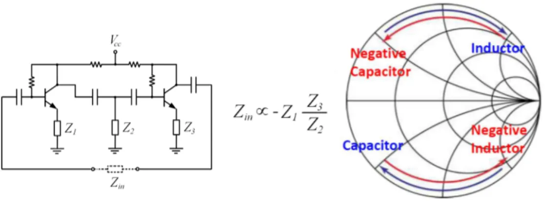
s shown in [1], it is in principle possible to widen the operation bandwidth of a passive MTM by loading it with an active circuit. In particular, in [1] a short dipole (or a small loop) antenna loaded with an ideal two-port electronic circuit has been considered and it has been shown that, in order to get negative and frequency-independent values of the permittivity (or permeability), it is necessary to use a negative capacitance (or inductance). In [1] it has been also suggested that this kind of reactive elements can be obtained using negative impedance converters (NICs), i.e. two-port devices exhibiting at the input port an impedance that is the opposite of the load one [2].
This class of active circuits, violating Foster’s theorem [3], has been introduced in the last century to compensate resistive losses [4] and their first transistor-based implementations are due to Linvill [5]. Recently, due to their unique and interesting properties, NIC circuits have been extensively applied to widen the operational bandwidth of electromagnetic components. For instance, as far as antennas are concerned, NICs have been used to design active external matching networks for both microstrip [6] and electrically small dipole/monopole/loop antennas [7]-[9] able to overcome Bode-Fano criterion, while a different conceptual approach, based on internal non-Foster matching circuits, has been proposed in [10]-[11]. Moreover, NICs have been used to synthesize ultra-wideband artificial magnetic conductors (AMCs) and electromagnetic band gap structures [12] and superluminal waveguides for broadband leaky-wave antennas [13]-[14].
In the last few years, some groups have focused their efforts to investigate the possibility of using NICs to overcome the limitations of passive MTMs. In particular, non-Foster elements have been used to increase the bandwidth of several types of broadband and electrically small MTM-inspired antennas [15]-[18] and to obtain an almost dispersionless epsilon-near-zero MTM, useful for cloaking applications [19]-[20]. Finally, in [21] an active broadband effective MTM has been proposed.
It is important to observe that, despite the potentials of such NIC circuits, their practical use is still limited, due to the fact that the design and the proper use of a NIC is not a trivial task. One of the main issues concerns the theoretical evaluation of the NIC stability and the related technological aspects. As clarified in [22], where several circuits including negative lumped elements have been investigated, in fact, the correct evaluation of the stability depends also on the used evaluation approach and the uncritical use of classical stability methods may result in assessment mistakes.
In this Chapter, inspired by the aforementioned papers, we propose to load an electrically-small antennas with a proper NIC-based active circuit, in order to increase its operation bandwidth and make it useful for the application in broadband MTM-inspired components. In order to show the potentials of the proposed broadband matching , we analyze the performance improvement of the SRR-based antenna presented in [23], suitably scaled to work within the RF band, where NIC implementation is not critical by using discrete circuit elements. The main result obtained, was to show that the operating band of the active devices of adaptation, based on non-Foster networks, can be increased considerably through the use of an appropriate NIC circuit, with discrete components on a single layer SMD technology. The Chapter is organized as follows: in Section 1, we introduce the general consideration of frequency band chosen for the project, advantage achieved by using the technology non-Foster matching for UWB applications where the radiating element can be electrically short; in Section 2, we describe a non-Foster technology and in Section 3, we introduce a technological scouting concentrated for possible NIC solutions circuit, this research was still conditioned and focused of broadband application to the conversion an electrically small radiating element load; in Section 4, we identify the technology and choice of NIC circuit solution; in Section 6 we describe the work to realize the basic support of a simulation model; in Section 7 we
introduce the activity regards the PCB design and circuit routing; in Section 8 we describe the industrialization and manufacturing NIC prototypes; in Section 9 we report the first RF characterizations on the two prototypes. Finally, Section 10, we deal with additional experimental test and future research activities
1.1
General consideration of frequency band chosen for the project
The portion of the spectrum up to now used for the radiopropagation has been limited to the range between 30 kHz and 300 GHz and , in this range , the portion more efficiently , and economically usable, is that of the 30 MHz to 3 GHz . In particular , within this range of frequencies they operate the most modern communication technologies ( Digital Audio Broadcasting DAB , DVB - T Digital Video Broadcasting Terrestrial , mobile 2G and 3G , Wi - Max , etc ... ) .
Fig. 1: Radio spectrum for modern broadcast communications technologies. In order to design the best way a radio communication , on a more or less wide band of frequencies , it is necessary to take into account the antenna radiation characteristics used and the type of service that the antenna must support . In practice it may be employed to type omniband (Wide Band or Ultra-Wide Band antennas ) such as to operate on a very wide band of frequencies by the use of non-resonant radiating elements , or alternatively it is possible to use multi-band antennas , realized with suitably loaded resonant radiating elements, such as to generate multiple resonance frequency bands.
The arrangement and the physical dimensions of the conductors that constitute and characterize the types of radiating element, are related to the practical use which is intended for the radio-link and the frequency band in which it is employed. One of the difficulties that have in practice is the realization of broadband radiating elements, compact and efficient, also operating in the extreme lower of the VHF band. Given the considerable size that would be to assume the resonant dipole in these frequency bands, generally are used antennas electrically very short (L/λ << 1), where the height L of the radiant element is generally reduced with the integration of lumped elements, creating current distribution discontinuities (by mean capacity or inductances along the antenna conductors).
In the technique of receiving systems, the non-Foster Matching technology has the ability to achieve higher instantaneous bandwidths and/or impedance matching of short antenna (than the wavelength of the signal wave taken as reference [24]-[25]. The usefulness of being able to work with a larger instantaneous bandwidth, is the ability to simultaneously and effectively receive signals on a wide frequency range, without antenna reconfiguration mode or changing tuning within the receiver.
Based on previous considerations, the advantage achieved by using non-Foster technology matching with radiating element metamaterial-based, can play a key strategic role in the search for the most suitable innovative solution [24] in the field of broadband receivers systems, characterized by innovative electrically short radiating elements, efficient in the Low-VHF- frequency band ( 30 - 50 MHz ).-
In order to realize an industrial product with non-Foster matching technology at low cost and easily reproducible, it is necessary to explore all practical requirements of an industrialized NIC solution, trying to estimate all possible unbalance associate at the nominal values of commercially discrete SMD (Surface Mount Technology) components and to delimit the inevitable parasitic effects associated with the circuit.
The parasitic components are associate to the proposed circuit solution, both to the process used for the realization of the product. It is therefore fundamental support of a simulation model throughout the cycle development product, reliable and robust, able to analyse and demonstrate the feasibility of the proposed circuit solution, and to verify and
optimize the functional parameters of the final solution, showing the expected performance.
The research was therefore focus on the study and the realization of a printed circuit NIC demonstrator realized in SMD discrete components with the following characteristics: compact, high integration and low cost production. Objective of this research is the design, realization and industrialization of an active NIC demonstrator, for Non-Foster Impedance Matching of Electrically small metamaterial-based antennas application.
The demonstrator has been design to be use in VHF / UHF broadband applications, for systems operating in the frequency band ranging from about 30 MHz to 3000 MHz (COMM band).
Starting from a technological scouting and some experimental work, it was identified a circuit and technological solution for the NIC discrete design. It ' was then carried out a search on the active and passive components required to implement the chosen circuit solution. In particular for this activity, starting from the Data Sheet from leading suppliers, it was necessary to check on the market, passive and active available component at low cost for civil applications.
For the active component identification was performed a detailed analysis and verification of the DC electrical characteristics (polarization working point and absorptions…) RF, (broadband matching, noise figure, stability...) and packaging.
In particular, with the ADS circuit simulator, it was made a qualitative analysis of the active circuit components and parasitic elements, and it was defined therefore to the circuit diagram of the NIC with the nominal values of selected SMD components.
The circuit model has obtained with using ADS simulator and through this, to verify the feasibility of the device.
For a quantitative analysis of the parasitic circuit components, the PCB model was realised using 3D full wave model CST MWS simulator.
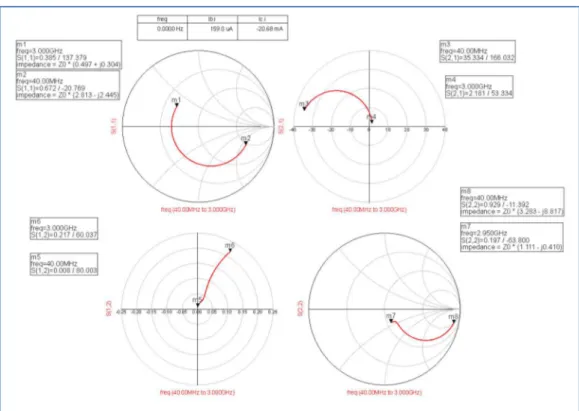
Finally, it was report the work done for the project and the PCB realisation, by the experimental results obtained on the two realized prototypes
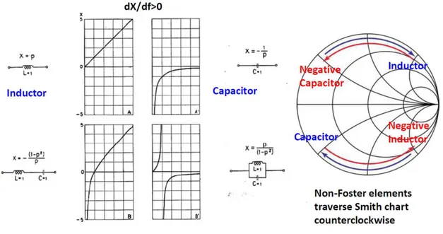
1.2
Non-Foster Technology
Foster's theorem is an important theorem for the analysis and synthesis of electrical networks. The theorem states that the reactance (imaginary part of complex electrical impedance) of a passive device with no losses to two terminals (or equivalently a passive network to a port) always has a monotonic behaviour with increasing frequency.
Fig. 2: Reactance behavior of Foster and Non-Foster networks type
The hypothesis that the network should be passive and lossless, implies that, in the network, there are no dissipative elements such as resistors, amplifiers or power sources. The network must therefore consist entirely of inductors and capacitors devices, where the impedance of the equivalent circuit will be purely an imaginary number.
Not all networks obey the th Foster theorem. For example networks containing amplifiers capable of creating negative capacitors and inductors by means of impedance conversion circuits NIC. These circuits are characterize by a positive reactance but with a negative slope trend in frequency.
1.3
Technology scouting for NIC solution
In the first phase of the research has been carried out a technological scouting concentrated for possible NIC solutions circuit. This research was still conditioned and focused application of broadband type but especially to the conversion of a "atypical load": the broadband impedance of the Electrically Small radiating element.
Electrically short antennas, in practice, have reactances capacitive with radiation resistance values very small and variable with the frequency.
Fig. 3: Equivalent circuit of an ideal electrically short dipole
For matching antenna, the classical approach provides the annulment of the negative reactance by the insertion of a tuned inductive network, while the resistive part of the network, transforms and adapts the output impedance characteristic of the receiver.
This approach can provide a single frequency adaptation condition and also implementing more complex passive networks, to R, L elements, and C, it is however very complicated - if not impossible - to cancel the reactive behavior of the electrically short radiant element impedance.
To solve the problem of adaptation and thus improve the radiation characteristics, two possible techniques have been designed to be integrated with each other.
• First approach is to use a negative impedance converter (NIC) formed by few discrete elements active and passive, so as to adjust the antenna reactance (with the parasitic components of the circuit itself), by means of specific components in the circuit monitored in voltage;
• Second method is to design the antenna in the same printed circuit board of the receiver and possibly exploit the properties of artificial materials or metamaterials to increase both radiative efficiency and to facilitate the mutual adaptation broadband between the two devices.