A 3D Vertically Integrated Deep N-Well CMOS MAPS for the SuperB Layer0
This article has been downloaded from IOPscience. Please scroll down to see the full text article. 2011 JINST 6 C01010
(http://iopscience.iop.org/1748-0221/6/01/C01010)
Download details:
IP Address: 193.204.248.133
The article was downloaded on 10/01/2011 at 08:53
Please note that terms and conditions apply.
View the table of contents for this issue, or go to the journal homepage for more Home Search Collections Journals About Contact us My IOPscience
2011 JINST 6 C01010
PUBLISHED BYIOP PUBLISHING FORSISSA
RECEIVED: October 16, 2010
ACCEPTED: December 14, 2010
PUBLISHED: January 5, 2011 TOPICALWORKSHOP ONELECTRONICS FORPARTICLE PHYSICS 2010,
20–24 SEPTEMBER2010, AACHEN, GERMANY
A 3D Vertically Integrated Deep N-Well CMOS MAPS
for the SuperB Layer0
G. Traversi,a,b,1L. Gaioni,b M. Manghisoni,a,b L. Rattib,cand V. Rea,b aUniversity of Bergamo,
Via Marconi 5, 24044 Dalmine (BG), Italy
bINFN Pavia,
Via Bassi 6, 27100 Pavia, Italy
cUniversity of Pavia,
Via Ferrata 1, 27100 Pavia, Italy
E-mail:[email protected]
ABSTRACT: Deep N-Well (DNW) Monolithic Active Pixel Sensors (MAPS) have been developed in the last few years with the aim of building monolithic sensors with similar functionalities as hy-brid pixels systems. In these devices the triple well option, available in deep submicron processes, is exploited to implement analog and digital signal processing at the pixel level. Many prototypes have been fabricated in a planar (2D) 130nm CMOS technology. A new kind of DNW-MAPS, namely Apsel5 3D, which exploits the capabilities of vertical integration (3D) processes, is pre-sented and discussed in this paper. The impact of 3D processes on the design and performance of DNW pixel sensors could be large, with significant advantages in terms of detection efficiency, pixel cell size and immunity to cross-talk, therefore complying with the severe constraints set by future HEP experiments.
KEYWORDS: Pixelated detectors and associated VLSI electronics; Analogue electronic circuits; Front-end electronics for detector readout
2011 JINST 6 C01010
Contents
1 Introduction 1
2 2D Deep N-Well CMOS MAPS 2
3 3D Deep N-Well CMOS MAPS 3
4 Conclusions 5
1 Introduction
CMOS monolithic active pixel sensors (MAPS) designed in standard VLSI CMOS technology have recently been proposed as compact pixel detectors for tracking applications at the next gen-eration colliders like the International Linear Collider (ILC) and SuperB Factory [1, 2]. MAPS are already extensively used in visible light applications: with respect to other competing imaging technologies, MAPS sensors have several potential advantages in terms of cost, power, noise and functionality. Figure1shows the cross-section of a CMOS sensor and its underlying basic princi-ple of operation. In most modern CMOS processes, n- and p-wells are fabricated on top of a thin p-doped epitaxial layer, with resistivity of the order of 1-10W·cm. A p-n junction exists between the n-well and the p-epi layer and can be used as the collecting element for the charge released by the radiation. In the extremely simple configuration of typical MAPS, only three transistors (3T) are integrated in the pixel cell, thereby providing fine spatial resolution. The use of large area electrodes is strongly discouraged in 3T-MAPS design: indeed, increased capacitance would unac-ceptably degrade the noise figure and the charge sensitivity at the same time. Moreover, the use of
Figure 1. Simplified cross-section of a CMOS pixel with epitaxial layer.
2011 JINST 6 C01010
PMOS devices in the front-end circuits of the pixel cell is to be avoided as their n-wells might sub-tract charge from the collecting electrode, leading to potentially serious efficiency loss. The lack of complementary devices represents a significant limitation to the design of stages with satisfactory properties, thereby restricting the set of available readout schemes. An innovative design solution for MAPS, leading to the so-called Deep N-Well (DNW) MAPS, was proposed a few years ago [3] in order to deal with the large amount of data produced in the readout of large matrices of pix-els. This solution relies upon the use of a deep n-well/p-substrate junction, provided by triple-well CMOS technologies, as the collecting element. DNW-MAPS allow designers to implement more complex readout circuits, taking advantage of fully CMOS architectures. However, although this approach is attractive because of the advantages of a full CMOS implementation, the overall detec-tion efficiency is adversely affected by the use of PMOS devices. In order to address this issue and to further improve such DNW MAPS properties as spatial resolution, new technology options have been recently considered, in particular, the interest of several research groups has shifted towards vertical integration processes (usually referred to as 3D) [4]. 3D processes, by stacking two or more layers one on top of the other, make it possible to improve DNW MAPS collection efficiency since PMOS can be placed in a different layer with respect to the sensor. Moreover, 3D processes may enhance functional density of the elementary cell and provide physical separation of the ana-log front-end from the digital blocks, thus preventing undesired cross-talk phenomena. The 3D IC Consortium [5] was promoted by Fermilab to explore 3D integration technologies. As a first step, European and US institutions submitted a multi-project wafer run in the Chartered-Tezzaron fabrication process. The Apsel5 3D chip, designed in the 3D IC framework, is the first generation of Deep N-Well CMOS monolithic sensors in a 130nm vertical integration technology. The main design features and the expected performance of the chip will be presented in section3.
2 2D Deep N-Well CMOS MAPS
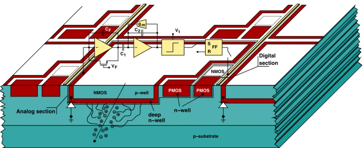
The DNW MAPS are based on the same sensing principle as standard MAPS, where radiation induced charge carriers diffuse and are collected by n-type electrodes. In a DNW MAPS sensor, whose structure is shown in figure2, an n-well with a deep junction acts as the collecting element for the charge released in the substrate. The collected charge is read out by a classical optimum chain for capacitive detectors, including a fully CMOS charge preamplifier whose closed loop gain is independent of the detector capacitance. The Deep N-Well, which in modern, triple-well CMOS processes is used to shield NMOS devices from substrate coupled noise in mixed signal circuits, may host n-channel devices, thus relaxing the constraints set by the readout circuits on the sensor area and geometry. Moreover, designers may implement more complex readout circuits, taking ad-vantage of fully CMOS architectures, laying out large area DNW sensors. Digital blocks involved in data sparsification and time stamping are also integrated in the elementary pixel cell. Several DNW sensor prototypes have been fabricated with the STMicroelectronics 130nm technology, de-veloped in view of their possible use in the innermost layer (Layer0) of the Silicon Vertex Tracker at the SuperB Factory [2]. The first prototypes included single pixel cells and small pixel matrices with a simple sequential readout. Characterization results have been published in [6,7] showing the viability of the concept. Apsel4D chip is the larger device of the Apsel family. It is a 32x128 matrix of 50x50µm2pixels with a continuous sparsified readout architecture based on macropixel
2011 JINST 6 C01010
Analog section Digital section R S FF deep n−well VF Vt C1 C2 CFNMOS PMOS PMOS
n−well p−well NMOS p−substrate + + + + + + + + + + − − − − − − − − − − gm
Figure 2. Conceptual drawing of the Deep N-Well MAPS structure.
(MP) cells (4x4 pixels). Each macropixel is connected to the periphery logic by two private lines used to send the hit information and receive the signal which freeze the MP until readout has been completed. Each pixel cell includes a collecting electrode and the full readout chain for signal processing shown in figure2. The Apsel4D chip has been fully characterized in laboratory and on a beam line in 2008 [8]. One of the most important results of the beam test is relevant to the detection efficiency of the matrix. A maximum efficiency of 92% was achieved at the threshold of about 400 electrons. Although this value is not compliant with the experiments specifications, it is consistent with device simulation of the sensor layout. Actually such a layout was not optimized with respect to competitive n-wells housing PMOS transistors. A new chip, including a new ver-sion of the elementary cell, has been fabricated and characterized with lab tests. Promising results have been obtained from laser tests and a beam test is foreseen in 2011.
3 3D Deep N-Well CMOS MAPS
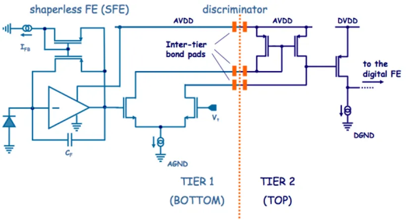
3D vertical integration technologies are extremely attractive for the development of monolithic pixel devices. A multilayer sensor structure may overcome typical limitations of MAPS fabricated in a planar technology. In a 3D DNW MAPS device, for example, a layer could host sensing electrodes and analog circuits while digital electronics could be located in the upper layer (see figure 3). In this way, most of the PMOS and their competitive N-wells are removed from the sensor layer, increasing the fill factor and therefore the detector efficiency. A multilayer structure allows also for a smaller pixel pitch and a smaller sensor capacitance, leading to better noise and power figures. Vertical integration also opens the possibility of using different technologies for the sensor (e. g.: high resistivity, detector-grade silicon) and for the readout electronics [4]. In the framework of the 3D IC Consortium [5] a vertically integrated DNW MAPS has been designed in the Chartered-Tezzaron process. The chip, now in fabrication, includes two 3x3 matrices for testing the readout electronics and the sensor performance (named Apsel5 3D). Apsel5 3D represents the evolution of the last prototype DNW monolithic sensor fabricated in a planar 130nm CMOS technology. The bottom tier of the Apsel5 3D elementary cell includes the Deep N-Well sensor, whose signal is processed by a charge sensitive preamplifier followed by a threshold discriminator
2011 JINST 6 C01010
Figure 3. Cross sectional view of a DNW CMOS MAPS: from a planar CMOS technology to a 3D process.Figure 4. Circuit schematic of the pixel cell in a DNW MAPS designed in a 3D vertical integration technol-ogy.
Figure 5. Signal at the output of the analog readout channel as a response to a charge pulse of 800 elec-trons. The waveforms were obtained from circuit simulations for different values of the current biasing the feedback current mirror.
only partially integrated in the bottom tier. The schematic circuit has the same scheme as in the elementary cell integrated in the planar 130nm CMOS technology (shown in figure4). The input NMOS device features a W/L=30/0.35 and a drain current of 20µA. Figure5shows the response,
2011 JINST 6 C01010
obtained from circuit simulations, of the analog chain to a 800 electrons charge pulse for different values of the current biasing the feedback current mirror. The expected charge sensitivity is close to 730mV/fC. A value of about 35 electrons has been obtained for the equivalent noise charge at a detector capacitance of 350fF. The threshold discriminator is based on a differential pair with PMOS active load and is followed by a common source PMOS gain stage. The area of the input differential pair and the PMOS active load is relatively large with respect to the other transistors in order to reduce the threshold dispersion as discussed in [9]. The PMOS active load and the second gain stage are integrated in the upper layer in order to reduce the area of the competitive N-wells in the sensor layer and therefore improving the charge collection efficiency. Device simulations based on Monte-Carlo methods show a detection efficiency of about 99% at a threshold setting of 400 electrons.
4 Conclusions
A large number of DNW CMOS MAPS have been fabricated with the planar 2D 130nm CMOS technology provided by STMicroelectronics. They implement a full in-pixel signal processing chain with the goal of approaching the requirements of the innermost layer (Layer0) of the Silicon Vertex Tracker at the SuperB Factory. The Apsel4D chip featuring in-pixel sparsification and pro-viding timestamp information for the hits has been fabricated and tested on a beam line. A new pixel cell with improved sensor layout has been tested with laser source and a beam test is foreseen in 2011. The use of a double-layer process in the development of the proposed DNW MAPS may address the main issues related to planar 130nm CMOS technology and dramatically improve the performance of the sensor in terms of functional density and charge collection efficiency. The de-sign of a new DNW MAPS sensor prototype in a two-layer, vertical integration process has been described. Several test structures have been integrated in the first multi-project wafer run in the framework of the 3D IC consortium to evaluate the suitability of the Chartered-Tezzaron technol-ogy for the fabrication of DNW MAPS. The 3D prototype delivery is expected by the end of 2010.
Acknowledgments
The authors wish to thank the SuperB SVT group and the members of VIPIX and SLIM5 collabo-rations for the hard and successful work carried out in the development of deep n-well monolithic active pixel sensors.
References
[1] M. Barbero et al., Development of a B-Factory Monolithic Active Pixel Detector - The Continuous Acquisition Pixel Prototypes,IEEE Trans. Nucl. Sci.52 (2005) 1187.
[2] The SuperB Conceptual Design Report, INFN/AE-07/02, SLAC-R-856, LAL 07-15, available online athttp://www.pi.infn.in/SuperB.
[3] L. Ratti et al., Monolithic pixel detectors in a 0.13um CMOS technology with sensor level continuous time charge amplification and shaping,Nucl. Instrum. Meth.A 568 (2006) 159.
2011 JINST 6 C01010
[4] R. Yarema, 3D IC Pixel Electronics - The Next Challenge, proceedings of Topical Workshop onElectronics for Particle Physics, 15-19 Sept. 2008, Naxos, Greece, pp. 183-187. [5] http://3dic.fnal.gov.
[6] G. Rizzo et al., Recent Development on Triple Well 130nm CMOS MAPS of Deep N-Well MAPS with In-Pixel Signal Processing and Data Sparsification Capability, IEEE Nucl. Sci. Symp. Conf. Rec. (2007) 927.
[7] L. Ratti, M. Manghisoni, V. Re, V. Speziali and G. Traversi, Non-standard approach to charge signal processing in CMOS MAPS for charged particle trackers,IEEE Nucl. Sci. Symp. Conf. Rec. (2005) 969.
[8] G. Rizzo et al., Development of Deep N-Well MAPS in a 130 nm CMOS Technology and Beam Test Results on a 4k-Pixel Matrix with Digital Sparsified Readout,IEEE Nucl. Sci. Symp. Conf. Rec. (2008) 3242.
[9] L. Ratti, Continuous Time-Charge Amplification and Shaping in CMOS Monolithic Sensors for Particle Tracking,IEEE Trans. Nucl. Sci.53 (2006) 3918.