High sensitivity measurement system for the direct-current, capacitance-voltage,
and gate-drain low frequency noise characterization of field effect transistors
G. Giusi, O. Giordano, G. Scandurra, M. Rapisarda, S. Calvi, and C. Ciofi
Citation: Rev. Sci. Instrum. 87, 044702 (2016); doi: 10.1063/1.4945263 View online: http://dx.doi.org/10.1063/1.4945263
View Table of Contents: http://aip.scitation.org/toc/rsi/87/4 Published by the American Institute of Physics
High sensitivity measurement system for the direct-current,
capacitance-voltage, and gate-drain low frequency noise
characterization of field effect transistors
G. Giusi,1O. Giordano,1G. Scandurra,1M. Rapisarda,2S. Calvi,2and C. Ciofi1
1University of Messina, I-98166 Messina, Italy 2IMM-CNR, I-00133 Rome, Italy
(Received 20 January 2016; accepted 18 March 2016; published online 5 April 2016; corrected 21 April 2016)
Measurements of current fluctuations originating in electron devices have been largely used to understand the electrical properties of materials and ultimate device performances. In this work, we propose a high-sensitivity measurement setup topology suitable for the automatic and programmable Direct-Current (DC), Capacitance-Voltage (CV), and gate-drain low frequency noise characterization of field effect transistors at wafer level. Automatic and programmable operation is particularly useful when the device characteristics relax or degrade with time due to optical, bias, or temperature stress. The noise sensitivity of the proposed topology is in the order of fA/Hz1/2, while DC performances are limited only by the source and measurement units used to bias the device under test. DC, CV, and NOISE measurements, down to 1 pA of DC gate and drain bias currents, in organic thin film transistors are reported to demonstrate system operation and performances. C 2016 AIP Publishing
LLC.[http://dx.doi.org/10.1063/1.4945263]
I. INTRODUCTION
Current-Voltage (IV) and Capacitance-Voltage (CV) measurements are the most common tools to investigate the electrical properties of classical and new electron devices.1–3 In addition to IV and CV, low frequency noise measurements (LFNMs) have been extensively used for the electrical characterization of electron devices, especially for Field Effect Transistors (FETs).2,3In this last case, the spectrum associated to the drain current fluctuations has been used to carry out an effective number of trap-density and to speculate about the physical origin of noise.4 With respect to other device
characterization methods (like IV and CV), Drain LFNMs have the major advantage of being not invasive as the device under test (DUT) is biased with a small amount of voltage drop, resulting in minor stress during measurement. Only recently (not induced), gate noise has been used to investigate material properties as a complementary tool to Drain LFNMs. Gate noise has the major advantage, with respect to drain noise, that it is sensible to defects located in the entire gate stack and not only close to the channel-oxide interface as is the case of drain noise.5–8Moreover, the normally negligible gate current makes gate noise not invasive as is the case of drain noise. However, LFNMs have the principal disadvantage, with respect to IV and CV, of a more complex setup mainly due to the necessity to have sufficiently high-sensitivity instrumentation and a sufficient system shield. Moreover, LFNMs can be more time consuming and more affected by change in environmental conditions. For these reasons IV, CV, and Gate/Drain LFNMs are complementary tools for device characterization, and measurement setups including all these features are required. Several drain noise systems have been proposed in the literature in the past5,9–13 and different systems are used in
research laboratories nowadays (like the BTA9812B noise
system14). While the level of sensitivity of such systems was
sufficient in the past, when only above-threshold conduction was investigated, nowadays other problems like subthreshold conduction in FETs or leakage conduction in memory devices, such as Metal-Insulator-Metal Capacitors (MIMCAP) or Resistive Random Access Memories (RRAM),15,16require the necessity to have more sensitivity noise systems. Other than sensitivity, another problem of measurement setups present in research laboratories is system integration. In fact, often, IV, CV, and NOISE tools are present as separate applications, while a comprehensive automatic and programmable system is required in many cases, for example, when the device char-acteristics relax or degrade with time. As an example, LFNMs can be used to monitor the bias/temperature stress of electron devices. In this case, fast and automatic switching between Direct-Current (DC) and NOISE operation is necessary, as well as the monitoring of DC and NOISE properties with time. Another example where the monitor with time and fast switching capability between DC and NOISE is necessary is related to Organic Thin Film Transistors (OTFTs), which have very high optical recombination time. This property causes a very slow relaxation of the IV characteristics after the device is illuminated to be contacted in the characterization system. In Ref. 17, we have presented a high-sensitivity automatic and programmable measurement system for IV and NOISE characterization of Drain current fluctuations. In this paper, we extend the system proposed in Ref.17including CV and low frequency noise (LFN) characterization of gate current fluctuations. Since the system allows contemporary Gate and Drain LFNMs, gate-drain cross-correlation18,19 can be used
to identify common causes of gate/drain current fluctuations. The general structure of the proposed system is presented in SectionII, while CV, IV, and LFN operations are discussed in SectionsIII–V, respectively. As the drain section has been
044702-2 Giusi et al. Rev. Sci. Instrum. 87, 044702 (2016)
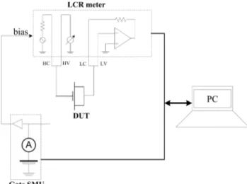
FIG. 1. Schematic diagram of the proposed setup for DC, CV, and LFN characterization of electron devices. In bold are the triaxial connections in the proposed system implementation (Sec.VI).
already discussed in detail in Ref.17, in this paper, we focus only on the improvements with respect to Ref.17, that is, CV and Gate NOISE operations. The actual implementation of the proposed system is reported in SectionVI. In SectionVII, CV and Gate IV/NOISE measurements in OTFTs20 are reported in order to demonstrate system performances.
II. SYSTEM DESCRIPTION
Fig. 1 shows the block diagram of the proposed setup. The DUT is connected to the system by a wafer station (probe station), which is enclosed, for noise and light shielding, into a metal box connected to the system ground. The main components of the system are three Source and Measurement Units (SMUs), an LCR meter, two custom-built Low Noise TransImpedance Amplifiers (LNTIAs),21and
a personal computer (PC) based spectrum analyzer (SA). Programmable switches (SW-G, SW-S, SW-D) are used to connect DUT terminals to SMUs during DC operation, to the LCR meter during CV operation, and to LNTIAs during NOISE operation. All system operations (including switches position and Drain LNTIA gain) are controlled by a PC to allow automatic and flexible characterization procedures. The LCR meter must use the auto-balancing bridge method (Fig.2) with a bias input for the DUT. LNTIAs are used to convert gate and drain current fluctuations to voltage fluctuations, which are measured by the SA, increasing the signal-to-noise ratio (SNR) at its input. SMUs are used to bias and measure DC currents at the three terminals during DC operation, to provide
the external bias to the LCR meter during CV operation, and to bias Gate and Drain LNTIAs during NOISE operation. As we will discuss in the following, this last feature allows to avoid the use of conventional low-noise battery-based bias systems and allows automatic and programmable operations under the main PC control.
III. CV OPERATION
During CV operation (Fig.2), the switch SW-G connects the gate terminal to both the HV (High Voltage) and HC (High Current) terminals of the LCR meter, the switch SW-D
connects the drain terminal to the LV (Low Voltage) terminal of the LCR meter, and the switch SW-S connects the source terminal to the LC (Low Current) terminal of the LCR meter. To provide the DC bias voltage to the DUT, the LCR meter is biased by the guard potential of the Gate SMU (VG). Since the DC potential at the terminals HV and HC is equal to VG, and LV and LC are both at virtual ground, the DUT is connected, to the LCR meter, as a gated diode as shown in Fig.2. Both the LCR meter and the Gate SMU are controlled via PC bus so that programmable CV operation (voltage sweep) is allowed.
IV. DC OPERATION
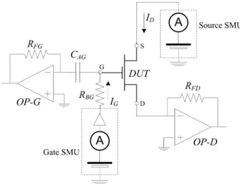
During DC operation, the switches SW-G, SW-S, and SW-D connect Gate, Source, and Drain DUT terminals to Gate SMU, Source SMU, and Drain SMU, respectively, to set voltages and measure currents (see Fig. 1). In principle, switches introduce leakage due to resistive and capacitive conduction between their terminals. However, as explained in the following, the terminals of switches are guarded (at the same potential) in order to minimize their DC leakage during DC current measurement. In fact, regarding the measurement of the gate current and the switch SW-G, the potential at the terminals HV and HC is equal to VG, and since CAGprevents any DC current into the Gate LNTIA, no DC leakage current can flow between the terminals of SW-G. Since the LCR meter is fed by the guard of the Gate-SMU, the Gate-SMU sources (and measures) only the device DC gate current. However, the capacitance CAGproduces a displacement leakage current, through SW-G, which is measured by the Gate SMU. For this reason, the gate current should be measured with sufficient delay time. Regarding the measurement of the drain current and the switch SW-D, the drain bias voltage (VD) is applied through the Drain SMU, but the LCR meter terminal LV and the input of the Drain LNTIA are at virtual ground, so that the switch SW-D is affected by DC leakage during DC operation. For this reason, the channel current is read by the Source SMU (which is set to 0 V) because the terminals of the switch SW-S are both at virtual ground and no leakage current flows between them. In this situation, DC performances (accuracy, resolution, and dynamics) are limited only by the SMUs and not by the system topology.
V. NOISE OPERATION AND ANALYSIS
During NOISE operation, the switches connect the gate terminal to the Gate LNTIA, the drain terminal to the Drain LNTIA, and the source terminal to the Source SMU as shown in Fig.3. The channel bias (VDS) is applied to the DUT through the Source-SMU since the drain terminal is at virtual ground through the input of the Drain LNTIA. However, the equivalent input voltage offset of OP-D causes a programming accuracy error in the channel bias so that calibration of the Source SMU voltage is required. The gate bias is applied through the Gate-SMU (CAG prevents any DC current flowing into the Gate-LNTIA). However, in order to take into account for the DC drop across RBG, during NOISE operation, the voltage of the Gate-SMU is set to RBGIG+ VGwhere (IG,VG)
FIG. 3. System configuration during NOISE operation.
is the DC bias point measured during DC operation (a DC measurement precedes any NOISE measurement). Normally, batteries are used to bias the DUT during LFNM because they do not add significant noise. However, this approach does not allow accurate and automatic biasing as in the proposed configuration. Moreover, with the proposed configuration, the Source-SMU can record (measure) the channel current during NOISE operation. As discussed in Ref.17for the drain section, and as discussed in the following for the gate section, in the proposed configuration, SMUs do not add significant current noise in situations of common interest. The bias voltage dynamics is limited by the SMUs voltage dynamics and by the feedback resistor RFD. In fact, neglecting DC errors, the DC voltage at the output of OP-D is Vout≈ −RFIDwhere ID is the channel current. If |ID| is sufficiently high, the large voltage drop across the feedback resistor can bring OP-D in saturation. In the proposed setup, RFD can be automatically selected, using switches, to be sufficiently low to prevent DC saturation but sufficiently high in order to set the appropriate background noise (BN) level.17
The drain low noise section has been discussed in detail in Ref. 17. Fig. 4(a) shows the Gate LFN section during NOISE operation (the DUT represents the gate-to-channel impedance). As for the drain section, the Gate LNA core is realized as a conventional opamp-based transimpedance amplifier consisting of a low noise opamp (OP-G) and a feedback resistance RFG. The feedback capacitance CFGis the cumulative effect of the parasitic capacitance of RFGand of the layout parasitic capacitance. The decoupling capacitance CAG introduces AC coupling (high pass filtering). If the impedance of the DUT is much large than RBG, the AC cutoff frequency is fAC≈(2πRBGCAG)−1. In the following, we will consider the AC behavior in the frequency range f ≫ fAC, where CAG can be considered a short-circuit. Fig.4(b)shows all relevant noise sources of the Gate-LNTIA in this situation. The DUT is represented with its equivalent (gate-to-channel) impedance ZDUT and a current noise generator iN,DUT, the opamp OP-G is schematized with its input current and voltage noise generators iN,OP-Gand eN,OP-G, the Gate-SMU is represented by an ideal voltage noise source eN,GATE, the DSA board is
044702-4 Giusi et al. Rev. Sci. Instrum. 87, 044702 (2016)
FIG. 4. (a) Gate-LNTIA section during NOISE operation; (b) noise model of the Gate-LNTIA.
represented by a voltage noise source eN,DSA, the bias resistor RBG is represented with its current noise generator iN,RBG, and the feedback resistor RFG is represented with its current noise generator iN,RFG. The capacitance CP represents the cumulative effect of the coaxial cable capacitance used to connect the gate to the LNTIA input, of the layout parasitic capacitance, and of the opamp input capacitance. The input referred current noise is
iN= iN,DUT+ iN,OP-G+ iN,RFG+ iN,RBG+ eN,DSA ZFG + eN,OP-G ZDUT//ZP//RBG//ZFG +eN,GATE RBG , (1)
where ZDUT, ZP, and ZFGare the small signal AC impedances associated to the DUT, CP, and to the feedback impedance, respectively. The input referred power spectral density (PSD) SINassociated to iNis then SIN= I2N,DUT+ SBN,G SBN,G= I2N,OP-G+ 4kT RFG//RBG+ E2N,DSA+ E2N,OP-G |ZFG|2 + E 2 N,OP-G |ZDUT//ZP|2 +E 2 N,GATE+ E 2 N,OP-G R2 BG + 2Re cN,OP-G ZFG//ZP//RBG//ZDUT , (2)
where I2N,DUT is the PSD associated to iN,DUT, SBN,G is the instrumentation background noise, E2N,DSA is the PSD associated to eN,DSA, E2N,GATE is the PSD associated to eN,GATE, I2N,OP-G and E2N,OP-G are the PSD associated to iN,OP-Gand eN,OP-G, respectively, and cN,OP-Gis the cross-spectrum (CS) between eN,OP-G and iN,OP-G. For typical values, the SBN,Gcan be approximated as
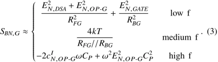
SBN,G≈ E2 N,DSA+ E 2 N,OP-G R2 FG +E 2 N,GATE R2 BG low f 4kT RFG//RBG medium f −2cIN,OP-GωCP+ ω2E2N,OP-GC 2 P high f . (3)
In Eq. (3), the range of “low f,” “medium f,” and “high f” is function of the parameters. In the “low f” range (typically ≪1 Hz), the BN is dominated by the flicker component of the voltage noise of the DSA, OP-G, and SMU Gate. At medium frequencies (typically 1-100 Hz), which is the typical measurement range, the BN is dominated by the thermal noise of the parallel RFG//RBG, so that both of them should be increased to minimize the BN. In this way also the low frequency BN reduces, including the current noise due to the gate bias (E2
N,GATE/R2BG). At high frequencies (typically >100 Hz), the BN increases, mainly due to the coupling between EN,OP-G and CP, limiting the useful measurement bandwidth. In order to reduce the high-f component of the BN, OP-G should have the lower voltage noise as possible, and efforts should be addressed to reduce CP using high-quality/short coax cables and reduce layout parasitic.
VI. SYSTEM IMPLEMENTATION AND VALIDATION
In the actual implementation of the proposed setup, the DUT is connected to the system by the probe station KARL SUSS PM5. Both the probe station and the low-noise sections are enclosed in metal boxes for noise shielding with respect to the system earth ground. Switches SW-G, SW-D, and SW-S are enclosed in the metal box together with the low noise sections. In order to minimize connection leakage, triaxial cables (in bold in Fig.1) are used to connect the SMUs to the switches, and from the switch SW-S to the Source DUT terminal. Gate and drain connections from the LNAs metal box (switches SW-G and SW-D) to the DUT (probe station metal box) are done with very short connectors in order to: (i) reduce the influence of external interferences; (ii) reduce the effect of the connection capacitance at the input of the Gate and Drain LNTIAs. Moreover, the chuck of the probe station is left floating (isolated from the ground) to avoid leakage and capacitance from a possible bottom contact in the wafer.
A. LCR meter
The LCR meter is the model GoodWill LCR-8110G, which uses the auto-balancing bridge method (see Fig.2). The sinusoidal test signal can have a maximum amplitude of 1 V, and the frequency can be selected in the range 20 Hz ÷ 10 MHz. The LCR-8110G allows to apply an external bias (up to ±200 V) to the DUT through the DC bias box model LCR-8000G. This feature allows to use a single SMU (the Gate SMU) to bias the DUT (gate) during DC, CV, and NOISE measurements as discussed in Secs. I–V. The LCR meter is interfaced to the PC through the IEEE 488 bus to allow automatic and programmable operations. We have measured,
after calibration, a residual capacitance (RC parallel model) with standard deviation in the order of 1 fF.
B. Source and measurements units
We used three of the four SMUs of the semiconductor parameter analyzer HP4155B. SMUs apply voltage and measure current at the gate, drain, and source terminals and are controlled, by the PC, through the IEEE 488 bus. Fig. 5 of Ref.17shows the measured voltage noise PSD at the output of a generic SMU of the HP4155B. As discussed in Ref.17, the low f component of the Drain SMU current noise is auto-filtered by the DUT impedance. On the other hand, since the gate voltage can have a large bias range (as in the case of OTFTs discussed later), the voltage noise produced by the Gate SMU can be much higher than the voltage noise produced by the Drain SMU, increasing the BN at the lower frequencies (Eq. (3)). From Eq.(3), this contribution can be reduced by increasing the value of RBG. In the proposed implementation RBG= 1 GΩ, and assuming a limiting maximum value of E2
N,GATE= 10−10 V2/Hz, the current noise produced by the Gate SMU would be E2N,GATE/R2BG= 10−38 A2/Hz, which is much lower than the current noise produced by RBGitself (∼10−29A2/Hz). In summary, due to the particular topology, Gate and Drain SMUs do not add significant noise contribution in situations of common interest. This property allows the use of SMUs in place of conventional batteries.
C. Low noise sections
The Drain LNTIA has been described in detail in Ref.17. The Gate LNTIA (Fig.4(a)) is AC coupled to the gate terminal and is connected to channel 3 of the DSA board. The opamp OP-G is the model TLC070, while RFG= RBG= 1 GΩ. Since CAG= 2.2 nF, in common situations where the gate impedance is much higher with respect to RBG, the AC cutoff frequency is fAC= (2πRBGCAG)−1≈ 0.1 Hz. Differently from the Drain LNTIA, the gate section has fixed and high transimpedance gain due to the low currents and noise expected at the gate terminal with respect to the drain terminal. The high transimpedance gain makes the DSA board noise (E2
N,DSA) usually negligible (Eq. (3)) so that a second (AC coupled) voltage gain stage is not necessary as it was the case for the Drain LNTIA. The switches are implemented with two sepa-rated relay modules (model SONGLE SRD-5VDC-SL-C). The low noise power supply for the LNTIAs is obtained by a couple of 6 V rechargeable lead acid batteries, providing ±6 V. The relay modules are powered with 6 V provided by the same battery group. Most of the power supply is required by the relay modules (∼80 mA/relay) so that, in order to reduce power consumption, when the system is in the idle state all relays are in their quiescent position. Batteries can be monitored and are recharged by the programmable power supply PS2521G, which is controlled, by the PC, through the IEEE 488 bus.
The input referred current PSD is calculated by dividing the measured voltage PSD by the transimpedance gain (|ZFD|2 or |ZFG|2). However, while the value of feedback resistance (RFDor RFG) is known with high accuracy due to the use of
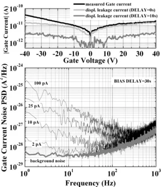
FIG. 5. (Top) Gate current vs. Gate voltage measured in OTFT (L= 2 µm, W= 70 µm, VDS= −1 V); (bottom) gate current noise PSD (black plots) for
different bias currents and background-noise of the Gate LNTIA (gray plot).
high precision resistors, the value of the feedback capacitance (CFD or CFG) is set by the layout parasitics and must be determined by proper measurements. In our realization we estimated, using the approach reported in Ref.22, a value of CFD≈ 4.5 pF and CFG≈ 5.4 pF. Fig.5 (bottom) shows the Gate BN (gray plot) when the DUT is not connected to the measurement system. At low frequency, the Gate BN is due to the thermal noise of 500 MΩ (the parallel between RFG and RBG) corresponding to ∼5 fA/Hz1/2, while at the higher frequencies, the BN increases due to the voltage noise of OP-G coupled with CPas expected from Eq.(3).
D. Spectrum analyzer
Spectrum analysis of measured current fluctuations is done by a common PC equipped with the DSA board model NI 4462, which has 4 independent acquisition channels with sampling frequency ( fs) up to 200 kS/s. The system bandwidth is then limited to 100 kHz since the analog section has a higher bandwidth due to the use of large gain-product opamps (TLC070). Spectra are calculated via software using the pe-riodogram Discrete Fourier Transform (DFT) algorithm. The software allows to specify all relevant acquisition parameters: bias voltages, sampling frequency, points per window, spectral window type, etc. As discussed in Ref.23, the accuracy error by using the DFT algorithm in 1/fγmeasurements could be particularly relevant for the first spectral points and increases with γ. Moreover, the estimation error is a function of the spectral window. For this reason, the frequency resolution should be chosen sufficiently low with respect to the first spectral point of interest in order to minimize the systematic DFT estimation error. We have found in Ref.23that, for γ ≈ 1, discarding the first 4 spectral points and using the Hanning
044702-6 Giusi et al. Rev. Sci. Instrum. 87, 044702 (2016)
window allows to have a negligible estimation error using the DFT algorithm. The noise measurement procedure is fully automated. The software follows the bias list specified by the user. For each bias point, DC currents are measured, as well as other relevant DC parameters (like the transconductance) are calculated. The DC point is measured before and after each measurement. This could be useful to check for possible DUT degradation during the noise measurement. Moreover, DC point info are used to set the correct gate voltage during NOISE operation, as discussed in SectionIV.
VII. DC, CV, AND NOISE MEASUREMENTS IN OTFTs
In order to demonstrate system performances, Gate DC, CV, and NOISE measurements in OTFTs20 have been
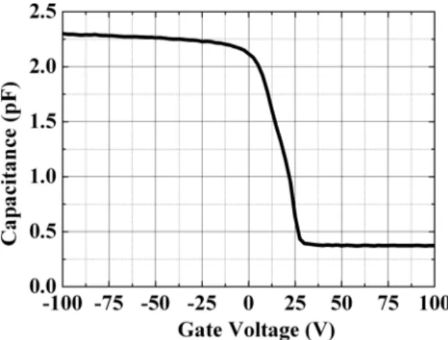
performed. Validation of the Drain IV and NOISE sections has been already reported in Ref. 17. DC and NOISE measurements (Fig.5) are related to a device with gate length L= 2 µm, gate width W = 70 µm, while the channel bias is VDS= −1 V (accumulation and linear regimes). Fig. 5 -top shows the gate current vs. gate voltage and the gate instrumentation leakage for two different DELAY times. As stated in Section IV, the large measured leakage current is due to the capacitance CAGand can be reduced, if necessary, increasing the DELAY time at the cost of a higher measure-ment time. Fig.5-bottom shows the gate current noise PSD. The measured noise follows a 1/ f behavior at low frequency, while at higher frequencies (∼100 Hz), the measured noise is dominated by the BN due to the CPcontribution as discussed in Sec. V. Due to the high sensitivity and low leakage of the proposed system, we were able to measure the Gate 1/f noise down to ∼1 pA of bias DC current. Fig.6 shows the gate-to-channel capacitance as function of the gate bias measured in a larger area device (as is commonly done in device characterization) with L= 100 µm and W = 220 µm. The LCR-meter sinusoidal-test-signal has an amplitude of 1 V and a frequency of 1 kHz and the capacitance is calculated using the parallel RC model. The measured gate capacitance is in the order of 10−12÷ 10−13F, which is much higher than the system residual capacitance (∼1 pF).
FIG. 6. Gate-to-channel capacitance vs. gate voltage measured in OTFT (L= 100 µm, W = 220 µm) by the proposed system.
VIII. CONCLUSION
In this work, we proposed a high-sensitivity measurement setup topology suitable for the automatic and programmable DC, CV, and Gate/Drain LFN characterization of FETs at wafer level. DC, CV, and NOISE measurements, down to 1 pA of DC gate and drain bias currents, in organic thin film transistors, have been reported to demonstrate system operation and performances. The system sensitivity is in the order of few fA/Hz1/2 in the low frequency region and is much better than what reported by other authors.5,9–13 For
instance, the (commercial) noise system BTA9812B14used in
many laboratories has a background noise level in the order of 0.5 pA/Hz1/2.
ACKNOWLEDGMENTS
This work has been funded by MIUR by means of the national Program PON R&C 2007–2013, project “Elettronica su Plastica per Sistemi Smart-disposable” (No. PON02_00355_3416798).
1D. K. Schroder, Semiconductor Material and Device Characterization, 3rd
ed. (Wiley-IEEE Press, 2006), ISBN: 978-0-471-73906-7.
2M. J. Deen and F. Pascal,J. Mater. Sci.: Mater. Electron.17(8), 549–575
(2006).
3S. Cristoloveanu, M. Bawedin, and I. Ionica,Solid State Electron.117,
10–36 (2016).
4E. Simoen and C. Claeys,Solid State Electron.43, 865–882 (1999). 5H. Rao and G. Bosman,J. Appl. Phys.106, 103712 (2009).
6J. Lee, G. Bosman, K. R. Green, and D. Ladwig,IEEE Trans. Electron Devices50, 2499 (2003).
7T. Contaret, K. Romanjek, T. Boutchacha, G. Ghibaudo, and F. Bœuf,Solid State Electron.50, 63–68 (2006).
8P. Magnone, F. Crupi, G. Iannaccone, G. Giusi, C. Pace, E. Simoen, and C.
Claeys, Ultimate Integration of Silicon (ULIS), 2008.
9A. Comeau, M. Aubin, and J. H. Orchard-Webb,Rev. Sci. Instrum.59, 955
(1988).
10A. A. Abidi,Rev. Sci. Instrum.59, 351 (1988).
11L. R. Chaar and A. D. van Rheenen,IEEE Trans. Instrum. Meas.43(4), 658
(1994).
12C.-Y. Chen and C.-H. Kuan,IEEE Trans. Instrum. Meas.49(1), 77–82
(2000).
13A. Blaum, O. Pilloud, G. Scalea, J. Victory, and F. Sischka, in Proceedings
of the 2001 International Conference on Microelectronic Test Structures (ICMTS)(IEEE, 2001), pp. 125–130.
14See http: //proplusdesignsolutions.com/temp-web/html/products-services-noisepro.htmlfor information about the BTA9812B noise system.
15G. Giusi, M. Aoulaiche, J. Swerts, M. Popovici, A. Redolfi, E. Simoen, and
M. Jurczak,IEEE Electron Device Lett.35(9), 942 (2014).
16Z. Fang, H. Y. Yu, J. A. Chroboczek, G. Ghibaudo, J. Buckley, B. De
Salvo, X. Li, and D. L. Kwong,IEEE Trans. Electron Devices59(3), 850 (2012).
17G. Giusi, O. Giordano, G. Scandurra, C. Ciofi, M. Rapisarda, and S.
Calvi, in IEEE Instrumentation and Measurement Technology Conference (IMTC) Proceedings(IEEE, 2015), pp. 2095–2100.
18M. Sampietro, L. Fasoli, and G. Ferrari, Rev. Sci. Instrum. 70, 2520
(1999).
19G. Giusi, C. Pace, and F. Crupi,Int. J. Circuit Theory Appl.37(6), 781–792
(2009).
20G. Giusi, O. Giordano, G. Scandurra, S. Calvi, G. Fortunato, M. Rapisarda,
L. Mariucci, and C. Ciofi,Electron. Device Lett.36(4), 390–392 (2015).
21G. Giusi, F. Crupi, C. Ciofi, and C. Pace, in IEEE Instrumentation and
Measurement Technology Conference (IMTC) Proceedings(IEEE, 2006), pp. 1747–1750.
22G. Giusi, G. Scandurra, and C. Ciofi,Rev. Sci. Instrum.85, 024702 (2014). 23G. Giusi, G. Scandurra, and C. Ciofi,Fluctuation Noise Lett.12(1), 1350007