Increasing the Immunity to Electromagnetic
Interferences of CMOS OpAmps
Anna Richelli, Luigi Colalongo, and Zsolt M. Kovács-Vajna, Senior Member, IEEE
Abstract—This paper presents the successful design of a CMOS operational amplifier with enhanced immunity to electromagnetic interferences. Thanks to its strongly symmetrical topology, the amplifier exhibits an intrinsic robustness to interferences arising from a wide class of sources. Such a scheme, for the first time in the authors’ knowledge, proves the effectiveness of symmetrical topologies to minimize the effects of electromagnetic interferences in operational amplifiers. The amplifier architecture is based on 2 identical stages: 2 fully differential source cross-coupled amplifiers with active loads. The circuit was fabricated in a 0.8 m -well CMOS technology (AMS CYE process). Experimental results, in terms of EMI immunity, are presented and compared with a commercial amplifier. They show a low susceptibility to EMI conveyed both to the input and the power pins. The EMI effects on the proposed amplifier are reduced by more than one order of magnitude, compared to a commercial amplifier. Furthermore the amplifier overall measured performances are provided along with the corresponding simulation results.
Index Terms—CMOS, electromagnetic interferences, opera-tional amplifier, parasitic effect, slew rate, symmetric topology.
ACRONYMS1
EMI electromagnetic interference IC integrated circuit
OpAmp operational amplifier output voltage bias voltage
GBW gain bandwidth product
SR slew rate
peak-to-peak voltage amplitude I. INTRODUCTION
E
MI EFFECTS can involve many electrical or electronic equipments along with interconnects. As an example, air-craft might be susceptible to electronic interferences because of their reliance on radio communication and navigation systems whose electromagnetic spectrum ranges from 10 kHz (naviga-tion systems) up to above 9 GHz (weather radar).Furthermore, the massive introduction of electronics in automobiles might cause many problems: e.g., cellular tele-phone transmitters can disturb braking systems (ABS). EMI might arise from inside the automobile as well: e.g., alternator,
Manuscript received January 17, 2002. Responsible Editor: R. M. Burger. The authors are with the Department of Electronics, University of Brescia, Italy (e-mail: [email protected]; [email protected]; [email protected]@ing.unibs.it).
Digital Object Identifier 10.1109/TR.2003.817847
1The singular and plural of an acronym are always spelled the same.
Fig. 1. Effect of the EMI conveyed to the input pin.
ignition system, switching solenoids, electric starter, and lamps, are potential sources of such disturbances.
Nowadays, because of the high density of components packed on printed circuit boards as well as the increasing speed of mixed analog digital circuits, IC designers have to consider EMI during their design phase. Neglecting these aspects might lead to failures on IC induced by spurious signals that might arise from a large class of sources, including EMI at frequencies outside the working bandwidth of the circuit [1]–[3].
Furthermore the lack of EMI immunity forces the IC de-signers to reduce circuit susceptibility by means of a posteriori layout adjustments, filters, change in the operating frequency, shielding, etc., that are seldom viable and are often complex and expensive. Therefore, in recent years, EMI were carefully investigated [3] both theoretically and experimentally to find possible prevention methodologies, in particular in high-perfor-mance digital/analog IC that might include several operational amplifiers [4]. The circuits most sensitive to EMI are the analog ones and, among them, the OpAmps [3].
Previous works [2], [3], assessed that the interfering signals might propagate mainly in 2 different ways: conduction and ra-diation. However, considering the chip size and the working fre-quencies of possible electronic systems, that act as EMI sources, the conduction seems at the moment the most relevant way of propagation.
Hence, to investigate the EMI effects on a generic amplifier, the interfering signals should be modeled by a waveform easily reproducible with a standard function generator. As reported in literature [3]–[5], the interfering signals are often represented by a sinusoidal waveform generated with a zero DC voltage source superimposed on the pins connected to long wires (long wires act as antennas for EMI).
One of the most undesirable effects of interferences is a shift of the output DC mean value (offset) that might asymptotically force the amplifier, or a subsequent stage, into saturation as shown in Fig. 1.
Furthermore, among all the possible interfering signals, the ones superimposed on the input pins of the operational amplifier are the most difficult to prevent. This is because the adoption of external filters might modify the original input signals that are often very weak. As far as the power pins are concerned, easy filtering can prevent the dangerous DC offset to be formed [6].
Fig. 3. Source cross-coupled amplifier.
Recently, much has been devoted to investigate the most im-portant causes of the anomalous drift to saturation of OpAmps when exposed to interference [5]. The EMI susceptibility has been correlated to some special features of the OpAmp transient responses. In particular, the asymmetric slew rate and the para-sitic capacitances are important. The asymmetric slew rate is im-portant at low-medium frequencies; the parasitic capacitances are relevant at high frequencies, outside the working bandwidth. Hence, in order to reduce EMI effects intrinsically, a promising approach is based on the design of strongly symmetrical topolo-gies.
This paper devises a highly symmetrical CMOS amplifier: its architecture allows EMI effects to be reduced by more than one order of magnitude, compared to commercial amplifiers.
Section II presents the circuit topology. Section III discusses the measurement results and compares them to a commercial amplifier.
II. AMPLIFIERARCHITECTURE
The overall OpAmp architecture is displayed in Fig. 2. It is based on 2 identical blocks, i.e., 2 fully differential source cross-coupled amplifiers, with current source loads. The 2 cir-cuital blocks are combined in cascade to achieve a large gain. Frequency compensation is obtained by means of two RC lines connected across the output buffer, as shown in Fig. 2.
Fig. 3 shows the circuital scheme of the source cross-coupled amplifier: this topology is very useful when the output slew rate of the OpAmp is important.
Such a scheme leads to a strong symmetry of the output voltage, thanks to the mirrored path of the signals.
Fig. 4. Chip microphotograph.
Indeed, as shown in Fig. 3, the input voltages are applied to the gates of both M2a and M2b, in order to bias the NMOS differential pair, and to the gates of M1a and M1b to bias the PMOS differential pair. NMOS and PMOS differential pairs are connected with cross-coupled sources. Hence, the input voltages of the first stage are symmetrically applied to the gates of the 2 differential pairs M3 and M4. In the same fashion, the output voltages of stage #1 are symmetrically applied to the gates of the 2 differential pairs of stage #2.
Thus, any voltage mismatch, due to stray elements and non-idealities, is removed by this cross connection. This leads to a very symmetrical path for both signals across the amplifier.
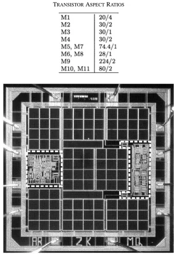
The circuit is fabricated in a 0.8 m n-well AMS CMOS CYE technology, thanks to the Europractice prototyping service.
Table I shows the transistor aspect ratios (in m).
With regard to this, it is important to point out that, thanks to the symmetrical topology, a precise sizing of the transistor aspect ratios is not mandatory in order to achieve a symmetrical slew rate (and a low EMI susceptibility). This is attractive for IC, when the process parameters might have slight fluctuations. The bias voltage is obtained from the supply voltage by means of 1 integrated resistive divider.
The values of the RC line elements, required for stability, are 5 K and 2.5 pF, respectively.
Fig. 4 shows a snapshot of the chip die. On the right hand side, the proposed amplifier is boxed in a dashed white line; on the left hand side of the die, the circuit of another OpAmp, not
Fig. 5. EMI measurement circuit.
connected to the proposed one, is boxed as well. The space be-tween the amplifiers is filled by capacitors connected bebe-tween Vdd and Vss, in order to minimize the susceptibility to the in-terferences arising from the power pins; the overall capacitance is about 3 nF. It is important that such a large capacitance can also be easily placed at the board level [6], because this filter is not critical at all.
III. MEASUREMENTSRESULTS
A. EMI Immunity
To investigate the EMI immunity level, the OpAmp was mea-sured in the voltage follower configuration as in Fig. 5; the in-terfering signals are modeled by sinusoidal waveforms applied to both the input and the power pins. The amplitude of the inter-fering signal was assumed to be , with 0 DC mean value. The frequency ranges from 100 kHz up to 4 GHz, to account for the spectrum of most of the current possible interfering signals, including the cellular phone bands.
Both the amplifier configuration and the interfering signal models represent a worst-case condition [3]. In the voltage fol-lower configuration, the direct connection, between the output and the inverting input node, forces the gates of the differential pair to experience the largest voltage difference. Furthermore the choice of an undamped sinusoidal waveform as an inter-fering signal represents a worst case condition as well, because the EMI interferences usually decay in time.
The experimental results, in the case of interfering signals applied to the input pin, are in Fig. 10; there, the offset voltage of the proposed amplifier is compared to the output offset of a commercial one. The OpAmp used as a reference in the figure is the well known A741. In [3] other amplifiers are listed that may be used as comparison as well.
The offset of our OpAmp, as shown in Fig. 10, is more than one order of magnitude smaller than the one of the A741 which, in turn, appears to be rather susceptible to EMI. It is important to note that the supply voltage of the A741 is 12 V, whereas the proposed amplifier supply voltage is only 2.5 V. Fig. 13 shows the offset as function of the amplitude. The offset appreciably increases when the interfering signal amplitude is a relevant fraction of the voltage supply.
As shown in Fig. 10, the output offset of our amplifier is about a few tens of millivolts in the whole frequency range. On the contrary, at frequencies slightly larger than the operating
band-Fig. 6. Pin model.
TABLE II
EMI MEASUREMENTSCIRCUITELEMENTVALUES
width, the A741 exhibits remarkable offset, of about 700 mV. The offset could easily drive the OpAmp to saturation with pos-sible failure of the system connected to its output.
At larger frequencies, the parasitic effects of the measurement set-up (board, cable, etc., act like a low-pass filter and the offset of both amplifiers decay to a value of few tens of millivolts.
With regard to the EMI measurement setup, the board in-terconnections were designed as short as feasible along with straight paths and ground shields, to minimize all the undesired signals arising from the measurement setup itself. For the same purpose, two 10 F and 100 nF capacitors were connected be-tween Vdd and gnd and bebe-tween Vss and gnd.
The output pins are connected to an RC filter in order to eval-uate their mean voltage, which easily and accurately quantifies the EMI effects.
Finally, the measurement board was shielded by an RF metal box.
The overall circuit element values are listed in Table II. Figs. 11 and 12 show the measurement results for an inter-fering signal applied to the positive and negative supply pins, respectively. The offset voltage of our amplifier is compared again to the A741; measures show an EMI immunity much larger than the commercial amplifier.
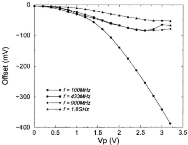
In order to clearly comprehend the EMI effects on OpAmps, Fig. 13 shows the offset of the proposed amplifier, at 4 different frequencies: 100 MHz, 433 MHz, 900 MHz, 1.8 GHz, with ranging from 200 mV up to 3.2 V (it is a large value, if compared to the supply voltage). Based on previous work and on computer simulations, one can expect a growing offset with the amplitude and the frequency of the interfering signals. On the other hand, as shown in Fig. 13, the amplifier behavior is remarkably dif-ferent from theoretical calculation, i.e., the measured offset does not build up monotonically neither for increasing amplitude nor for increasing frequency as expected.
A possible explanation of such behavior can be found n OpAmps nonlinearity concerning the amplitude response, in the parasitic effects of both bonding and package, and in
Fig. 7. Transient response to a square wave.
Fig. 8. Positive slew rate.
Fig. 9. Negative slew rate.
the measurement set-up, that often acts as a low pass filter, concerning the frequency response.
To evaluate the parasitic effects arising from the packaging (pins, bonding, etc.) a lumped model like the one in Fig. 6 can be used. On the other hand, the approximation introduced by lumped models is often too severe and unsuitable for an intrin-sically distributed effect like the one dealt with here.
Fig. 10. EMI applied to the input pin (measurements).
Fig. 11. EMI applied to the Vdd pin (measurements).
TABLE III
MAINFEARURES OFTHEOPAMP
B. Amp Characterization
To characterize an operational amplifier, the measurement of several typical parameters such as, dc gain, supply cur-rent, unity gain bandwidth, slew rate (positive and negative), common mode rejection ratio (CMRR), power supply rejection ratio (PSRR), should be performed.
Table III summarizes the main measured features of the am-plifier, and compares them with those obtained by the circuit simulator Spectre before fabrication. A good agreement was found.
Fig. 12. EMI applied to the Vss pin (measurements).
Fig. 13. Output offset as a function of interfering signal amplitude and frequency.
TABLE IV SET OFINSTRUMENTS
Table III shows that the Gain of the proposed OpAmp is about 63.5 dB, the GBW is 12.5 MHz, the power consumption is about 10 mW, and the slew rates (both positive and negative) are 25 V/ s. Both of the absolute values of CMRR and PSRR, positive and negative, are satisfactory.
Figs. 7–9 show the transient responses to the square wave in the slew rate conditions. It is important that, as emphasized by the oscilloscope images, the positive and negative slew rates of the proposed OpAmp are strongly symmetrical.
The overall die size is 2.2 mm 2.2 mm, but the amplifier core area is much smaller (200 m 1000 m). Fig. 4 shows that a large fraction of the die area is filled by capacitors and by another independent circuit.
Table IV lists the overall set of used instruments. ACKNOWLEDGMENT
The authors appreciate the support in device fabrication pro-vided by Europractice. They would like to thank S. Graffi, G. Masetti, and E. Sardini for their suggestions and encourage-ments on this work.
REFERENCES
[1] C. R. Paul, Introduction to Electromagnetic Compatibility: John Wiley & Sons, 1992.
[2] A. S. Poulton, “Effect of conducted EMI on the DC performances of operational amplifiers,” Electronics Letters, vol. 30, pp. 282–284, 1994. [3] G. Masetti, S. Graffi, D. Golzio, and Z. M. Kovács-Vajna, “Failures duced on analog integrated circuits from conveyed electromagnetic in-terferences: A review,” Microelectronics and Reliability, vol. 36, no. 7/8, pp. 995–972, 1996.
[4] G. Setti and N. Speciale, “Design of a low EMI susceptibility CMOS op-erational amplifier,” Microelectronics and Reliability, vol. 38, p. 1143, 1998.
[5] G. Masetti, G. Setti, and N. Speciale, “On the key role of parasitic ca-pacitances in the determination of susceptibility to EMI of integrated operational amplifiers,” in Proc. EMC1999 Zurich, 1999.
[6] Z. M. Kovács-Vajna, E. Sardini, and N. Speciale, “Chaotic behavior of 741 OpAmps subjected to EMI conveyed to power supply rails,” in Proc.
ISCAS2000 Geneva, vol. 1, May 2000, pp. 727–730.
Anna Richelli was born in 1974 in Brescia, Italy. She received the Laurea de-gree in Electronic Engineering in 2000 from the University of Brescia, Brescia, Italy. She is working toward her Ph.D. at the Department of Electronics for Au-tomation, University of Brescia. Her main research interests include design of analog circuits with immunity to electromagnetic interferences and integrated step-up converters.
Luigi Colalongo was born in 1965 in Bologna, Italy. He received the aurea degree in Electronic Engineering from the University of Bologna Italy, and the Ph.D. in Electronic Engineering and Material Science from the University of Trento, Italy. From 1991 to 1999, he worked at the Department of Electronics of the University of Bologna (DEIS). He is an Assistant Professor at the University of Brescia, Italy, and is engaged in an activity on the numerical simulation of semiconductor devices and in integrated circuit design.
Zsolt M. Kovács-Vajna (M’90–SM’00) received his Laurea degree summa cum
laude in 1988 and his Ph.D. in 1994 in Electronics Engineering and Computer
Sciences from the University of Bologna, Italy, for his work on optical character recognition and circuit simulation techniques. He was a Visiting Researcher (1988–1994) and Assistant Professor in Electronics (1994–1998) at the Depart-ment of Electronics Engineering of the same University. He is an Associate Pro-fessor in Electronics at the Department of Electronics for Automation, Univer-sity of Brescia, Italy, and teaches the course “Microelectronics.” His research interests include integrated circuit design for sensor applications, pattern recog-nition (OCR, ICR, fingerprint identification, innovative pointer devices) and electromagnetic interference analysis in integrated circuits. Dr. Kovács-Vajna is author or coauthor of 2 books, of more than 70 scientific papers in edited books, international journals, and conference proceedings, and of 5 patents.