Dedicated to the people who fill my life everyday
i This thesis reports a study of several two-dimensional supramolecular networks deposited on gold surface and two-dimensional materials. The work aims to evidence the formation of the molecular assemblies and their related interaction with the underling substrates.
First, the metal-organic interface between Zn(II) tetraphenyl porphyrin (ZnTPP) and Au(111) is systematically characterized as a function of the molecular coverage. We found that the interaction between the gold surface and the molecular monolayer is considerable, unlike one might expect from this particular system. Moreover, the molecular diffusion process is also evidenced.
Afterwards, the self-assembly of the Nile red molecules on Au(111) substrate, from sub- to mono- layer coverages, is reported for the first time. The dependence of molecular packing from the thermal treatments of the samples is evidenced, while further information are also gained on the intermolecular interaction and on molecular mobility.
Later, supramolecular assembly of two carboxylic acids, i.e. benzene-1,4-dicarboxylic acid (terephthalic acid, TPA) and benzene-1,3,5-tricarboxylic acid (trimesic acid, TMA) deposited on graphene substrate were investigated. After determining the monolayer packing, the structural transition that occurs as molecular deposition proceeds over the monolayer coverage is determined. We evidence that, despite the chemical similarity between the two molecules, their monolayer-to-thin-film transitions are dramatically different.
Finally, the effect of the deposition of the electron acceptor 7,7,8,8-tetracyanoquinodimethane (TCNQ) molecules on the surface of a prototypical topological insulator, i.e. bismuth selenide (Bi2Se3), is reported. The molecular assembly was determined, while a negligible charge transfer between the molecular layer and the substrate are also found.
In addition to the main topic of the work, the thesis also reports other research activities connected to the two-dimensional systems. In particular, the growth and characterization of graphene films on copper foil, by means of Chemical Vapor Deposition (CVD) are performed. The different coupling of graphene layer on the Cu foil and the possibility to induce a variation of the graphene coupling with respect to the Cu substrate by visible-light irradiation above a proper power threshold are evidenced. Finally, the nucleation and growth of iron cluster on MgO/Ag(100) surface is considered. Relevant information are obtained on the cluster size dependence from deposition temperature of the substrate and from the nominal coverage.
Keywords: Scanning tunneling microscopy (STM), X-ray photoelectron spectroscopy (XPS), self-assembly, supramolecular architectures, graphene, topological insulator, chemical vapor deposition, Raman spectroscopy, metal clusters.
ii Questa lavoro di tesi riporta uno studio di diversi assemblati molecolari bidimensionali depositati su superfici di oro e su materiali bidimensionali. Il lavoro si propone in particolare di evidenziare sia la formazione degli assemblati molecolari che la loro interazione con i substrati sottostanti.
Pe p i a osa, l’i te fa ia etallo ga i a t a la Zi o-Tetrafenilporfirina (ZnTPP) e la superficie cristallina di Au(111) è stata sistematicamente caratterizzata in funzione del ricoprimento molecolare. L’i te azio e sti ata t a la supe fi ie dell’o o e il o ost ato ole ola e è o side evole, più di ua to ci si potesse aspettare da questo particolare sistema.
I seguito, vie e ipo tato, pe la p i a volta, l’auto-assemblaggio delle molecole di Rosso Nilo sulla superficie di oro, al variare del ricoprimento molecolare, ovvero dal ricoprimento parziale della superficie fino al monostrato molecolare. In parti ola e, è stata evide ziata la dipe de za dell’i pa hetta e to molecolare dai trattamenti termici dei campioni, mentre ulteriori informazioni sono state ottenute sulle interazioni intermolecolari e sulla mobilità molecolare.
A seguire, gli auto-assemblati ole ola i di due a idi a ossili i, ovve o l’a ido te eftali o TPA e l’a ido t i esi o TMA so o stati studiati sulla supe fi ie di g afe e. Dopo ave dete i ato l’i pa hetta e to molecolare del monostrato, è stata evidenziata inoltre la differente transizione strutturale che si verifica quando la deposizione delle molecole procede oltre la copertura del monostrato.
I fi e, vie e ipo tato l’effetto della deposizio e di ole ole a etto i di elett o i, ovve o il TCNQ, su u isolante topologico, ovvero il bismuto selenio (Bi2Se3). L’a alisi effettuata ha o se tito di dete i a e l’i pa hetta e to ole ola e, ed ha ulte io e te esso i evide za un trasferimento di carica trascurabile tra lo strato molecolare e il substrato.
Oltre al tema principale del lavoro, la tesi riporta anche altre attività di ricerca connesse ai sistemi bidimensionali. In particolare, sono state eseguite la crescita e la caratterizzazione di film di grafene su fogli di rame (Cu), mediante Deposizione Chimica da Vapori (CVD). Il differente accoppiamento dello strato di grafene sul foglio di Cu e la possibilità di indurre una variazione dell'accoppiamento di grafene rispetto al substrato stesso mediante irradiazione di luce visibile, al di sopra di una ben determinata soglia di pote za, so o stati evide ziati i seguito all’a alisi effettuata. Infine, viene considerata la nucleazione e la crescita di cluster di ferro sulla superficie di ossido di magnesio (MgO) cresciuto su Ag (100). Informazioni rilevanti sono ottenute sulla dipendenza dalle dimensioni del cluster dalla temperatura di deposizione del substrato e dalla copertura nominale.
Parole chiave: Microscopia a Scansione Tunnel (STM), spettroscopia fotoelettronica a raggi (XPS), auto-assemblaggio, architetture molecolari, grafene, isolante topologico, deposizione chimica da vapore, spettroscopia Raman, cluster metallici.
iii Abstract (English/Italian) i Contribution vii
Introduction
1 References 41. Methods
71.1 Scanning Tunneling Microscopy 8
1.1.1 Quantum Tunneling 9
1.1.2 Bardeen approximation 11
1.1.3 STM imaging 14
1.2 Scanning Tunneling Spectroscopy (STS) 15
References 17
Part I: Molecular Self-Assembly
182. STM and XPS investigation of ZnTPP adsorption on
19Au(111) surface: from monolayer to multilayer transition
2.1 Introduction 20
2.2 Experimental section 22
2.3 Results and discussion 23
2.3.1 STM investigation of ZnTPP self-assembly 23 on Au(111) at Room Temperature
2.3.2 XPS investigation of ZnTPP coverage 29
dependence on Au(111)
34 36 37 2.4 Surface diffusion of the ZnTPP 2nd layer
2.5 Conclusions References
iv
3.1 Introduction 44
3.2 Experimental section 44
3.3 Results and discussion 47
3.3.1 Nile Red assembly at submonolayer coverage 47 3.3.2 Monolayer Regime of Nile Red on Au(111) 50
3.3.3 Nile Red mobility 58
3.4 Conclusions 59
References 61
4. TMA and TPA self-assemblies on graphene
634.1 Introduction 64
4.2 Experimental section 66
4.3 Results and discussion 68
4.3.1 Monolayer structure of TMA and TPA on HOPG and 68 graphene
4.3.2 Resolving the structure of TMA thin-films 72 4.3.3 Structural transition in TPA thin-films 78
4.4 Conclusions 81
References 82
4.5 Appendix section 85
5. TCNQ physisorption on the Bi2Se3 Topological Insulator
995.1 Introduction 100
5.2 Experimental section 101
5.3 Results and discussion 102
5.4 Conclusions 106
References 107
v
6. Coupled and freestanding behaviour of monolayer
115
aa
graphene deposited by low pressure CVD (LP-CVD) on Cu foil
6.1 Introduction 116
6.2 Experimental section 117
6.3 Results and discussion 118
6.3.1 Monolayer graphene coupling on Cu foil 118
6.3.2 Laser-induced transition from coupled- to 128 freestanding- graphene
6.4 Conclusions 132
References 133
7. Characterization of graphene grown on copper foil by
137aa
Chemical Vapor Deposition (CVD) at ambient pressure
aa
conditions
7.1 Introduction 138
7.2 Experimental section 139
7.3 Results and discussion 141
7.4 Conclusions 148
References 150
7.5 Appendix section 153
Part III: Metal clusters on metallic surface
1558.
Nucleation and growth of iron clusters on MgO/Ag(100)
1568.1 Introduction 157
8.2 Nucleation and growth 157
8.2.1 Clusters irreversible growth 159
8.2.2 Ostwald and Smoluchowski Ripening 161
8.3 Nucleation and growth of Fe clusters on MgO/Ag(100) 164
8.3.1 Experimental setup 164
vi
References 172
9. Conclusions and outlooks
174References 175
Acknowledgements
178vii
I. Co-Authorship Declaration
This thesis incorporates material that is result of joint research, as follows:
Chapter 2: The XPS measurements were acquired at Elettra Syncrotron (APE beamline) and analysed by Dr. Marco Papagno, Dr. Daniela Pacilé (Department of Physics – Università della Calabria, Italy) as well as her PhD student Ilenia Grimaldi.
Chapter 4: The AFM, TEM results, as well as the graphene grown on the copper foil and successive transfer on the TEM grid, were gained by Dr A. J. Marsden, Z. P. L. Laker under the supervision of the Prof. N. R. Wilson at the Department of Chemistry – University of Warwick (UK)
Chapter 5: The Bi2Se3 samples were synthetized under the supervision of Dr. E.V. Chulkov at the
Saint Petersburg State University. STM data were acquired and analysed by Dr. Ada Della Pia at the Giovanni Costantini laboratory – Department of Chemistry – University of Warwick (UK), while the DFT calculation was performed by Dr. A. Arnau (Donostia International Physics Center (DIPC), Donostia-San Sebastian, Spain)
Chapter 6 - 7: The Raman acquisitions and analysis was performed in collaboration with the Raman spectroscopy group (Prof. Enzo Cazzanelli, Dr. Marco Castriota) – Department of Physics – Università della Calabria (Italy) and with the Prof. G. Mariotto – Department of Computer Science – Università di Verona (Italy).
Chapter 8 reports the experimental results collected during my PhD stage at the École Polytechnique Fédérale de Lausanne (EPFL) – Prof. Harald Brune research group.
I have obtained the permission from each of the co-author(s) to include the above material(s) in my thesis. I certify that, with the above qualification, the thesis, and the research to which it refers, is the product of my own work.
viii preparation) reported below.
Thesis chapter
Publication title/ Full citation Publication
status Chapter 2 STM a d XPS investigation of Zinc(II) tetraphenylporphyrin
Z TPP adsorptio o Au surfa e . O. De Luca, T. Caruso, I.Grimaldi, D.Pacilé, A. Policicchio, V. Formoso, M. Papagno and R.G. Agostino.
In preparation
Chapter 3 I estigatio of Nile Red self-assembled monolayer on Au . T.Caruso, O. De Luca, M. Turano, A. Ionescu, N., Godbert, A. Policicchio and R.G. Agostino.
In preparation
Chapter 4 Mo olayer-to-thin-film transition in supramolecular asse lies: the role of topologi al prote tio . A. J. Marsden, Z. P. L. Laker, O. De Luca, A. Della Pia, L. M. A. Perdigao, G. Costantini, N. R. Wilson. Nanoscale, 2017, 9, 11959–11968
Published*
Chapter 5 TCNQ physisorptio o the Bi Se topologi al i sulator . A. Della Pia, S. Lisi, O. De Luca, D. Warr, M. M. Otrokov, Z. S. Aliev, E. V. Chulkov, R. G. Agostino, A. Arnau, M. Papagno and G. Costantini.
Submitted
Chapter 6 Differe t spe tros opi eha ior of oupled a d freestanding graphene monolayer deposited by CVD on Cu foil . E. Cazzanelli, M. Castriota, A. Fasanella, R. Grillo, O. De Luca, A. Policicchio, G. Desiderio, R.G. Agostino, M. Giarola, and G. Mariotto.
In preparation*
Chapter 7 Chara terizatio of graphe e gro o opper foil y Chemical Vapor Deposition (CVD) at ambient pressure o ditio s . E. Cazzanelli, O. De Luca, D. Vuono, A. Policicchio, M. Castriota, G. Desiderio, M. P. De Santo, A. Aloise, A. Fasanella, T. Rugiero, R. G. Agostino.
Accepted
*The publication (published or in preparation) is included inside the chapter. However, some sections of the same chapter are not comprised in the publication.
Other related publications that this thesis is not directly based on but where I have contributed as an author are listed below:
1. FeP Adsorptio o the Moiré Superstru ture of Graphe e I ter alated With a Co Layer . G. Avvisati, S. Lisi, P. Gargiani, A. Della Pia, O. De Luca, D. Pacilé, C. Cardoso, D. Varsano, D. Prezzi, A. Ferretti, and M. G. Betti. J. Phys. Chem. C, 2017, 121 (3), pp 1639–1647. 2. Che i al o d and charge transfer dynamics of a dye-hierarchical TiO2 hy rid i terfa e .
C. Castellarin-Cudia, T. Caruso, E. Maccallini, A. Li Bassi, P. Carrozzo, O. De Luca, A. Goldoni, V. Lyamayev, K. C. Prince, F. Bondino, E. Magnano, R. G. Agostino, C. S. Casari. J. Phys. Chem. C, 2015, 119 (16), pp 8671–8680
ix Dr. Marco Papagno, Dr. Daniela Pacilé – Department of Physics – Università della Calabria, Italy Prof. Giovanni Costantini – Department of Chemistry – University of Warwick, UK
Prof. Enzo Cazzanelli, Dr. Marco Castriota – Department of Physics – Università della Calabria, Italy
Dr. Nicolas Godbert, Dr. Andreea Ionescu – Department of Chemistry – Università della Calabria, Italy
Dr. Maria Penelope De Santo – Department of Physics – Università della Calabria, Italy
Dr. Danilo Vuono – Department of Chemical and Environmental Engineering – Università della Calabria, Italy
1 Synthesizing and controlling advanced functional nanostructured materials and devices is one of the most important scientific challenges to be faced in the next years. The development of these next-generation devices promise to revolutionize several fields in which they will find application, including electronics, physics, chemistry, biology and medicine.
In order to realize these functional materials, the nanofabrication methods are divided into two major categories, i.e. the top–do a d the otto –up approa hes. While the top-down method allows creating nano-functional devices with the desired shapes and characteristics starting from larger dimensions of the components and reducing them to the required values, by using several lithography methods[1-3], the otto -up fa ri atio ai s to reate
multifunctional nanostructured materials and devices by the self-assembly of atoms or molecules.
The most obvious advantage of the last methodology concerns the possibility to directly control the atomic or molecular assemblies. Some of the most prominent bottom–up nanofabrication methods include atomic layer deposition,[4] sol–gel nanofabrication,[5] vapor phase deposition of
nanomaterials[6] and molecular self-assembly.[7] Among the last techniques, self-assembly of
molecular compounds was well-acknowledged as one of the efficient bottom-up approaches to synthesize various materials with controllable architectures and novel properties.[8-11]
Molecular self-assembly (MSA) is the process by which molecules assemble themselves without the presence of outside interactions.[12,13] Relevant examples of self-assembly structures are
present in nature, including the formation of the lipid bilayer of the membranes of cells, the cellular membranes and the folding and aggregation of peptides and proteins. In order to create new types of supramolecular networks, the most versatile and prominent MSA strategy is based on the Self Assembled Monolayers (SAMs) approach. As a matter of facts, SAMs represent one of the most effective strategy for surface functionalization. As a result, in these last years, a huge amounts of organic molecules were deposited on the semi-conductors, noble metal surfaces and two dimensional materials in order to achieve this goal.
The synthesis and growth of such two-dimensional architectures is driven by the interplay of intricate intermolecular and molecule-substrate interactions. If on one hand the stability and the order of the molecular networks arise from the ensemble of multiple intermolecular non-covalent interactions such as hydrogen bonding,[14,15] van der Waals forces,[16] hydrophobic and
2 substrate influence the final assembly and consequently the resulting surface functionalization.
Indeed, molecular self-assemblies strongly bonded to the surface, i.e. through chemical bonding, allows to strictly modify its properties. For instance, a much studied system is the case of thiol networks on metal surfaces,[26-28] where molecules are bonded to the solid substrate by a reactive
head that provides a strong molecule–substrate bond. Conversely, the non-covalent self-assemblies show a weak interaction with the surface (including hydrogen bonds and van der Waals interaction), i.e. in this particular case, molecules are physisorbed on the underlying substrate. The surface functionalization by means of weak interacting molecular assemblies shows obvious advantages with respect to the covalent one. Firstly, the surface properties can be functionalized by the self-asse ly depositio ithout he i ally odify the su strate, that is, in other words, the pristine surface is preserved. Furthermore, the lacking of anchored groups allows to investigate the molecular cores, which express a precise functionality because directly interacting with the surfaces. In addition, the surface can also e e ployed as a i ert template in order to study the molecular self-assembly and the mechanisms underlying its formation.
In that background, the main purpose of this thesis is to investigate non-covalent self-assemblies of organic molecules on noble metals and two-dimensional materials, as reported in the Part I of this work. In particular, Scanning Tunneling Microsopy (STM) technique allows us to determine the molecular organization of self-assembled networks with an atomic resolution. Moreover, the electronic properties of molecular networks can also be obtained by using X-ray Photoemission Spectroscopy (XPS). Combined analysis of STM imaging and XPS measurements permit to obtain deep information regarding the molecular packing structure, from submonolayer to few- layers coverage, and the interaction between the supramolecular network and the substrate. In particular, Chapter 2 reports the investigation performed on the zinc-tetraphenylporphyrin (ZnTPP) molecular network on the Au(111) surface. Relevant information about the molecular packing and the molecules-substrate interaction were gained by using a combined STM and XPS analysis. Furthermore, the formation of the molecular second layer, in terms of growth and molecular mobility, was also investigated. In Chapter 3 the self-assembly of the Nile red molecules on the Au(111) substrate, from sub- to mono- layer coverages, was reported for the first time. STM imaging and semi-empirical calculations performed on this system allow to gain
3 intermolecular bonding. In Chapter 4 the supramolecular assembly of benzene-1,4-dicarboxylic acid (terephthalic acid, TPA) and benzene-1,3,5-tricarboxylic acid (trimesic acid, TMA) deposited on graphene were investigated. Combining STM, electron diffraction and acTEM imaging, the structural transition that occurs as molecular deposition proceeds was evidenced, and the critical thickness beyond which the film structure is no longer defined by the molecular 2D crystal at the substrate surface is determined. Despite the chemical similarity between the two molecules, their monolayer-to-thin-film transitions are dramatically different. Chapter 5 reports the effect of the deposition of the electron acceptor 7,7,8,8-tetracyanoquinodimethane (TCNQ) molecules on the surface of a prototypical topological insulator, bismuth selenide (Bi2Se3). STM
investigation allows to determine the molecular packing, while the photoemission spectroscopy measurements demonstrates a negligible charge transfer between the molecular layer and the substrate.
All the investigated cases represent model systems that allow us to study both the molecular assemblies of the molecules, as a function of the particular compound and substrate, and the interaction with the surface. Furthermore, in some cases the evolution of the molecular film beyond the monolayer case is also presented.
In addition to the main topic of the work, the thesis also reports other research activities performed during the PhD course, still related to the two-dimensional systems. In particular, Part II describes the growth and characterization of graphene films on copper foil, by means of Chemical Vapor Deposition (CVD). Chapter 6 reports the possibility to induce the a variation of the graphene coupling with respect to the Cu substrate by visible-light irradiation above a proper power threshold, while Chapter 7 both evidences the dependence of the graphene film quality by varying the exposure time to the carbon flux and two distinct graphene films, at the same time, on the copper substrate.
Finally, Part III, which contains only the Chapter 8, reports the nucleation and growth of iron clusters on MgO/Ag(100) surface. Here, relevant information were obtained on the cluster size dependence from deposition temperature of the substrate and from the nominal coverage.
4 [1] B. D. Gates, Q. Xu, M. Stewart, D. Ryan, C. G. Willson and G. M. Whitesides, Chemical
Reviews 105 (4) (2005): 1171-1196
[2] S. P. Li, D. Peyrade, M. Natali, A. Lebib, Y. Chen, U. Ebels, L. D. Buda, and K. Ounadjela, Physical Review Letters 86(6) (2001): 1102.
[3] D.S. Ginger, H. Zhang and C. A. Mirkin, Angewandte Chemie International Edition 43(1) (2004): 30-45.
[4] H. Kim and W.J. Maeng, Thin Solid Films 517(8) (2009): 2563-2580.
[5] M. R. Weatherspoon, Y. Cai, M. Crne, M. Srinivasarao and K. H. Sandhage, Angewandte Chemie International Edition 47(41) (2008): 7921-7923.
[6] A. Reina, X. Jia, J. Ho, D. Nezich, H. Son, V. Bulovic, M.S. Dresselhaus and J. Kong, Nano Letters 9(1) (2008): 30-35.
[7] L. C. Palmer and S. I. Stupp, Accounts of Chemical Research 41(12) (2008): 1674-1684. [8] G.M. Whitesides and M. Boncheva, Proceedings of the National Academy of Sciences 99(8) (2002): 4769-4774.
[9] J. Zhang, Y. Li, X. Zhang and B. Yang, Advanced Materials 22(38) (2010): 4249-4269. [10] Y. Li, L. Liu, R. Subramani, Y. Pan, B. Liu, Y. Yang, C. Wang, W. Mamdouh, F. Besenbacher and M. Dong, Chemical Communications 47(32) (2011): 9155-9157.
[11] L. Piot, D. Bonifazi and P. Samorì, Advanced Functional Materials 17(18) (2007): 3689-3693. [12] S. Zhang, Nature Biotechnology 21 (10) (2003): 1171-1178.
[ ] S.A. DiBe edetto, A. Fa hetti, M. A. Rat er a d T. J. Marks. Ad a ed Materials ‐ (2009): 1407-1433.
[14] S. Clair, S. Pons, A. P. Seitsonen, H. Brune, K. Kern and J. V. Barth, The Journal of Physical Chemistry B 108, no. 38 (2004): 14585-14590.
[15] W. Xu, M. D. Dong, H. Gersen, E. Rauls, S. Vàzquez-Campos, M. Crego-Calama, D. N. Reinhoudt, I. Stensgaard, T. R. Linderoth and F. Besenbacher, Small, 2008, 4(10),1620–1623. [16] H. Ascolani, M. W. van der Meijden, L. J. Cristina, J. E. Gayone, R. M. Kellogg, J. D. Fuhr and M. Lingenfelder, Chemical Communications 50(90) (2014): 13907-13909.
[17] G. Tomba, M. Stengel, W. D. Schneider, A. Baldereschi and A. de Vita, ACS Nano, 2010, 4, 7545–7551.
[18] N. Abdurakhmanova, A. Floris, T. C. Tseng, A. Comisso, S. Stepanow, A. de Vita and K. Kern, Nature Communication , 2012, 3, 940.
[19] S. Stepanow, R. Ohmann, F. Leroy, N. Lin, T. Strunskus, C. Woll and K. Kern, ACS Nano, 2010, 4, 1813–1820.
[20] L. Cui, X. Miao, L. Xu, Y. Hu and W. Deng, Physical Chemistry Chemical Physics 17(5) (2015): 3627-3636.
[21] A. E. Baber, S. C. Jensen and E. C. H. Sykes, Journal of the American Chemical Society 129(20) (2007): 6368-6369.
[22] A. C. Papageorgiou, A. Alavi and R. M. Lambert, Chemical Communication, 2012, 48, 3394– 3396.
5 [24] Z. Shi, T. Lin, J. Liu, P. N. Liu and N. Lin, CrystEngComm 13, no. 18 (2011): 5532-5534.
[25] A. Kumar, K. Banerjee and P. Liljeroth, Nanotechnology 28(8) (2017): 082001. [26] D.I. Rozkiewicz, B.J. Ravoo and D.N. Reinhoudt, Langmuir 21(14) (2005): 6337-6343. [27]M. Lessel, O. Bäumchen, M. Klos, H. Hähl, R. Fetzer, M. Paulus, R. Seemann and K. Jacobs, Surface and Interface Analysis 47(5) (2015): 557-564.
[28] V. Y. Kutsenko, Y. Y. Lopatina, L. Bossard-Giannesini, O. A. Marchenko, O. Pluchery and S. V. Snegir, Nanotechnology 28(23) (2017): 235603.
Methods
This chapter describes the main experimental technique used in this thesis, scanning tunneling microscopy (STM). The working principle, the theory of quantum tunnelling and the STM spectroscopic mode will be discussed in detail.
8
1.1 Scanning Tunneling Microscopy
The invention of the scanning tunneling microscope (STM) has revolutionized the field of microscopy, providing for the first time resolution down to the atomic scale. It was developed in 1981 by Binnig and Rohrer, awarded five years later by the Nobel Prize, at the IBM labs in Zurich.
The ability to resolve the surface at atomic level, related to its local electronic properties, and the opportunity to obtain further information on the local density of states (LDOS) by the spectroscopic mode (STS – Scanning Tunneling Spectroscopy), make the STM a fundamental investigative technique in the nanotechnology field.
The working principle of the STM is relatively straightforward. It uses a sharp metal tip to probe the sample and to image its surface. By applying an appropriate voltage between the metallic tip and the (conductive) sample, a current flows from the tip to the sample (or vice versa), when their distance is in the order of 0.5-1nm. This quantum tunneling current, classically forbidden, allow gaining fundamental information about the electronic properties of the surface.
The STM tip fine movements towards the surface and in the lateral direction can be controlled with high precision by a piezoelectric scanner tube with electrodes, which can contract or extend under the action of an applied voltage. A schematic view of an STM is shown in Fig. 1.
9
1.1.1 Quantum Tunneling
The basic phenomenon of the STM is the quantum tunneling of electrons between two electrodes separated by a thin potential barrier. The simplest case of tunneling through a potential barrier occurs for a particle in one dimension (1D), as shown in Fig. 2.
Figure 2. Schematic representation of the electron tunneling through a potential barrier (1D-case).
Consider an electron with energy that is incident on a potential barrier such that
In the 1-dimensional case, the Schrödinger wave equation is given by
− ħ
𝑥 + z = .
where is the wave function, ħ the reduced Planck constant, the mass of the electron, the time-independent potential and the energy of the particle.
The solutions to the Schrödinger equation for the wavefunction in the barrier region, in the case < , are given by
𝑧 =∝ − 𝑧 , = √ − ⁄ .ħ
where ⁄ is the lengthscale of the potential barrier at which tunneling can occur. The vacuum potential barrier represents the energy needed to remove an electron from the
10 material, i.e. the work function. In the STM case, its typical value ranging from 3 to 5 eV. As a consequence, the typical tunneling lengthscale is − ~ Å.
The probability that an electron passes through the potential barrier, having height and thickness , is given by
| 𝑧 = | ∝ − .
As a result, the width of the potential barrier must be approximately ~ − for electrons to tunnel across the barrier. For this reason, the STM tip must be near to the surface in order to measure a tunneling current. Moreover, the exponential dependence of (1.4) means that if − ~ Å, for Å change in vertical direction the tunneling probability increases by an order of magnitude.
The tunneling probability in (1.4) is directly related to the tunneling current. As a consequence, as a first approximation, the tunneling current scales exponentially with the barrier width . In the particular case of STM, the potential barrier lies between the tip and sample, which are located to a distance . A schematic representation of the energetic landscape of an electron that moves along a metallic-substrate/insulator/metallic-tip tunneling junction is shown in Fig. 3.[2]
Figure 3. Energy profile the electrons moving along a tip-vacuum-sample junction. 𝑧 is the surface
normal direction while is the tip-sample distance. 𝜙 , and , are the work functions and the Fermi levels of tip and sample, respectively. The gray boxes represent the Fermi-Dirac distribution at 0 K. (a) At equilibrium, a trapezoidal potential barrier is created between the two electrodes. (b) At positive and (c) negative sample bias, the electrons tunnel between the junction from the tip to the sample and vice versa, respectively. Figure adapted from [2].
11 At equilibrium, the tip and sample have the same Fermi level while their work functions, 𝜙 and 𝜙 respectively, are generally different (i.e. different materials). As a result, a trapezoidal potential barrier between the two electrodes is created, which is higher than the typical thermal energy of the electrons. Although particles can pass through the tip-sample barrier for the quantum tunneling effect, in the absence of a voltage applied between the two electrodes there is no net charge flow, i.e. tunneling current, in a particular direction. Conversely, by applying a polarized (or bias) voltage between the tip and sample, and adopting the convention for which the voltage is applied to the sample while the tip is grounded, the Fermi level of the sample is shifted by − and a net tunneling current occurs, whose direction depends on the sign of (see Figure 3(b) and (c)). In the case > , the electrons tunnel from occupied states of the tip into unoccupied states of the sample. As a consequence, imaging at positive bias allow investigating the conduction band, or the analogous Lowest Unoccupied Molecular Orbitals (LUMOs) in organic chemistry, of the sample. On the contrary, the valence band or the Highest Occupied Molecular Orbitals (HOMOs) of the sample can be investigated at negative bias, when the tunnelling current flows from the occupied states of the sample towards the empty ones of the tip. Clearly, electrons near the Fermi level have a higher probability to pass through the potential barrier.
1.1.2 Bardeen approximation
Ba dee s odel fo tu eli g i metal-insulator-metal junctions[3,4] can be transferred to the
STM case to gain the expression of the tunneling current 𝐼 . The basic idea is to consider the electronic structure of the tip and sample separately, as an unperturbed system described by two stationary one-particle Schrödinger equations:
+ = .
+ = .
where is the electron kinetic energy, and the unperturbed wave functions, and the electron potentials and and the energy of the particles.
The Fermi golden rule gives the transition probability per unit time of an electron that passing from the sample state to the tip state
12 = ħ | | ( − ) .
where is the matrix element
= ∫ ∗ 𝒙 𝒙 𝒙 𝒙 .
The total current will be given by the sum of over all the possible tip and sample states, multiplied for the electron charge
𝐼 = ∙ ∑
,
.
After introducing the density of states , the summation in (1.8) can be replaced by an energy integral
∑
,
→ ∫ .
where the factor 2 accounts for the spin degeneracy, while f is the Fermi-Dirac distribution function,
= − ⁄ B
+ .
in which is the Fermi energy, B the Boltzmann constant and the temperature. (1.10)
takes i to a ou t Pauli s e lusio p i iple a d the ele t o i state populatio at fi ite temperatures.
Assuming that the matrix element does not depend strongly on two particular states ( → ), the total current can be written as
𝐼 = ħ ∫ [+∞ − + − + ] − + +
−∞ | | .
where is the Fermi energy and the indexes and refer to the tip and the sample, respectively.
13 A more manageable expression of the tunneling current can be obtained in the low temperature limit ≪ , where the Fermi-Dirac distributions can be approximated by step functions. The resulting current became
𝐼 = ħ ∫ 𝑉 − + + | | , > .
𝐼 = ħ ∫ − + +
− |𝑉| | | , < .
Despite this last consideration, the tunneling current expression is still not easy to solve because the calculation of the matrix elements is too complicated. However, a satisfactory approximation can be obtained by considering that the tunneling current flows only between the last atom of a perfectly sharp tip and the surface atom directly underneath, in the small bias voltage range (+-2V).[5] In this case, | | can be expressed by a simple one-dimensional
WKB tunneling probability, while the probability that an electron with energy tunnels through a potential barrier 𝑧 of arbitrary shape, in WKB approximation[6] is given by:
= 𝑥 {− ħ∫ √ 𝑧 − 𝑧} .
Considering a squared barrier of average height rather than a trapezoidal one, as shown in Fig. 3,
𝜙 = 𝜙 + 𝜙 + ⁄ .
the (1.13) equation became
= 𝑥 {− √ ħ (𝜙 − ) } = 𝑥 − .
The (1.15) relation shows as the actual probability that an electron pass through a potential barrier depends strongly on the distance between the tip and the sample. Due to this exponential dependence, small variations of distance (~0.1 nm) lead to large changes in the tunneling current (around one order of magnitude). This behavior evidences the high vertical resolution of STM.
14 The substitution of the tunneling probability for the squared matrix element in the total current expression > leads to the relation
𝐼 = ħ ∫ 𝑉 − + + − .
As shown in equation (1.16), the tunneling current strictly depends on the sample-tip distance , applied bias and the tip and sample density of states ( and respectively). In particular, the density of states refer to the last atom of the tip and to the corresponding atom of the surface, in the Lang approximation.[5] As a consequence, can be
referred to the local density of states (LDOS).
1.1.3 STM imaging
STM allows imaging at constant current and constant height modes. In the first case, the voltage applied on the z piezo-element is continuously adjusted through a feedback circuit, so that the tunneling current is set to the same value. During the scanning of the surface the tip-sample distance changes in order to maintain a constant current value. This mode is the most frequently used. On the contrary, in the constant height mode the bias applied on the piezo along the z direction is kept constant, while the tunneling current variations are monitored. In this case, the tip-sample distance is kept constant while the current changes result from variations of the tip-sample distance. This imaging mode can be used only in very small areas and for flat samples, in order to avoid the tip crash on the sample.
15
1.2 Scanning Tunneling Spectroscopy (STS)
Beyond imaging, STM allow gaining spectroscopic information on the local electronic properties of surfaces with high spatial resolution. The STM spectroscopic mode (STS) give access to both the occupied and non-occupied states of the sample by changing the polarity of the bias voltage. As a result, STS can be considered in this sense a complementary technique respect to the Ultraviolet Photoemission Spectroscopy (UPS), with the additional advantage to investigate the electronic properties of the surface at small scale. As shown in equation (1.16), the tunneling current only depends on the bias voltage and on the tip-sample distance . This dependence can be used in a STS experiment, where the relation between two of these three parameters is measured while the remaining one is kept constant. As a result, three spectroscopic modes can be employed in an STS experiment: the 𝐼 , 𝐼 and spectroscopies. Among them, 𝐼 spectroscopy is the most widely used spectroscopic mode because it provides information about the local density of states (DOS) of the sample. In this case, the tip-sample distance is kept constant (i.e. the feedback control is disabled) while the tunneling current is measured as a function of the bias voltage. The differential conductance for a positive sample bias is obtained by differentiating the total current 𝐼 (equation 1.16) at a constant tip-sample separation, as shown by (1.17)
𝐼
∝ + , , + ∫ 𝑉 − + + , ,
+ ∫ 𝑉 − + + , ,
The 𝐼/ dependence on the sample local density of states (LDOS) in contained in the first term, while the other two terms show the voltage dependence of the transmission coefficient and the tip DOS , respectively. However, the equation . can be simplified by assuming small bias voltages and constant . In this case, the second term can be neglected while the third one vanishes, respectively. The resulting relation is given by
𝐼
∝ + , , .
As a consequence, the differential conductance can be considered a good representation of the sample density of states (LDOS) under the assumption of small voltages and constant , because the monotonous dependence of on ensures that any possible structure in 𝐼/
16 is only due to the voltage dependence of . In the case of higher biases, the voltage dependence of cannot be neglected. In this case, the normalized differential conductivity, i.e. 𝐼/ / 𝐼/ , is a better representation of ,[8] as both the numerator and
denominator depend on the tunneling probability . Although this procedure lacks a robust mathematic base, a good experimental agreement is found between the sample LDOS and the normalized differential conductivity especially in the case of semiconductors.[9]
17
References
[1] http://www.iap.tuwien.ac.at
[2] A. Della Pia and G. Costantini. "Scanning tunneling microscopy." Surface Science Techniques. Springer Berlin Heidelberg, 2013. 565-597.
[3] J. Bardeen, Physical Review Letters 6(2) (1961): 57.
[4] A.D. Gottlieb, L. Wesoloski, Nanotechnology 17(8), R57 (2006). [5] N.D. Lang, Physical Review B 34(8) (1986): 5947.
[6] L.D. Landau, E.M. Lifshitz, Quantum Mechanics. Non-relativistic Theory (Pergamon Press, Oxford, 1977).
[7] Ø. Fischer, M. Kugler, I. Maggio-Aprile, C. Berthod and C. Renner, Reviews of Modern Physics 79(1) (2007): 353.
[8] J.A. Stroscio, R.M. Feenstra, A.P. Fein, Physical Review Letters 57(20) (1986): 2579. [9] M. Passoni, F. Donati, A.L. Bassi, C.S. Casari, C.E. Bottani, Physical Review B 79(4) (2009): 045404.
18
STM and XPS investigation of ZnTPP adsorption on Au(111) surface:
from monolayer to multilayer transition
Bottom-up self-assemblies of organic molecules offer the most realistic solution toward the fabrication of next-generation functional materials and devices. In this chapter we present a focused investigation on the monolayer assemblies of a particular porphyrin, i.e. the zinc-tetraphenylporphyrin (ZnTPP), on the Au(111) surface. A combined analysis of STM imaging and XPS measurements allows to gain fundamental information about the molecular packing, the molecules-substrate interaction as well as the intramolecular interaction. Furthermore, essential information are also gained by the formation of the molecular second layer, in terms of growth and molecular mobility of the second ZnTPP layer.
20
2.1 Introduction
Assemblies of molecular architectures on metal surfaces are appealing systems due to the possibility of synthesizing advanced functional nanostructured materials and devices through molecular manipulation. The structure and stability of the well-ordered and two-dimensional molecular crystal grown is determined by the molecule-molecule and molecule-surface interactions. The resulting features of these materials significantly depend on the properties of the molecules-metal interface, which in turn are tightly connected to the interaction between the particular organic/inorganic components used. Molecules-surface interactions can in fact affect the shape of the adsorbed molecules[1] and their electronic structure[2-4] as
well as their magnetic properties.[5,6] In particular, the deposition of electron donor or
acceptor molecules allow to create interfaces with well-defined electronic properties, which can be employed in several fields.
Among all organic compounds, porphyrins are a well-known and versatile popular class of molecules, which has attracted over the years the attention for their significant electronic, optical and biological properties exploitable in a wide range of emerging technologies including field-effect transistors,[7-10] dye-sensitized solar cells,[11-14] sensors,[15,16] organic light
emitting diode[17-20] and synthetic bio-mimetic devices.[21,22] A noteworthy porphyrin
derivative is tetraphenylporphyrin (TPP), which consists of a porphyrin macrocycle with four phenyl groups bound to the pyrrole subunits by a carbon bridge. TPP molecules, with or without the metal transition atom (Ni, Co, Fe, Zn, Cu) base at the center, exhibit a prominent self-assembling behavior on noble metal surfaces such as Au(111),[23-28] Ag(111),[29-34] and
Cu(111)[35-37] as well as on TiO
2[38] even at room temperature.
As a result of the adsorption, these molecules typically form a stable molecular packing driven by the interaction on the plane between the phenyl groups, and the resulting unit cell is typically nearly square, where the porphyrin macrocycle stays either flat and parallel or distorted on the metal surface.[35,39-44] The molecular arrangement and the adsorption
geometry of these systems have been extensively studied in the last years by using Scanning Tunnelling Microscope (STM) and Near Edge X-Ray Absorption Fine Structure (NEXAFS) techniques.
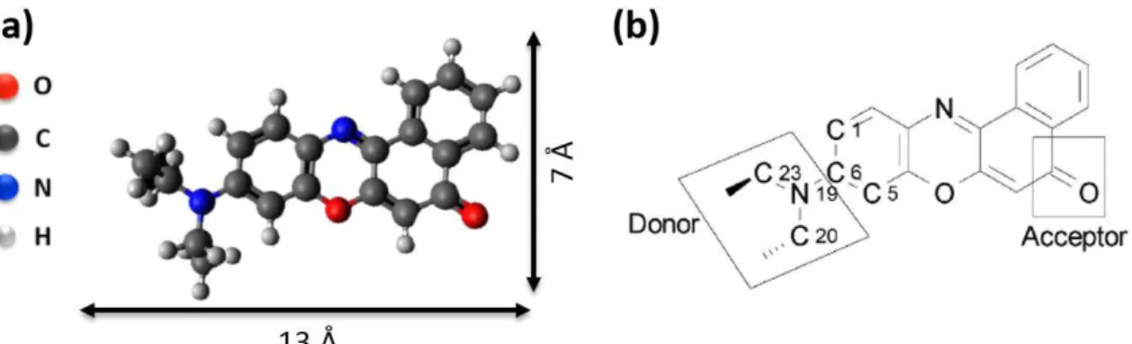
Bearing all this in mind, in this chapter, we investigate the adsorption of the Zinc(II) tetraphenylporphyrin (ZnTPP) (see molecular structure in Fig. 1) on the Au(111) substrate by using scanning tunneling microscopy (STM) and X-ray photoemission spectroscopy (XPS).
21 Although this system was already studied by means of STM,[23,24,26] a combined analysis of
microscopic and electronic investigations is still lacking. STM and XPS measurements allow to gain essential information about the interaction between the ZnTPP molecules and Au(111) surface. In particular, STM imaging shows that the typical herringbone (HB) reconstruction of the Au(111) disappears when the molecular overlayer is present on the surface. This electronic rearrangement of the gold substrate, which can be seen in terms of anisotropic surface stress,[45] is in fact an obvious signal of the significant interaction between the molecules and
substrate. XPS core level and valence band measurements also confirm this finding. The chemical shifts of the N1s and Zn3d core levels clearly indicate a considerable interaction of ZnTTP molecules on Au(111) in the few-layers regime, supporting as well the charge dishomogeneity revealed by the STM imaging, which also does not exclude an asymmetrical shape of the ZnTPP molecules on the gold substrate. In addition, the mono- to bi- layer transition is examined, which shows that the second layer was epitaxially formed on the ZnTPP monolayer. Furthermore, the molecular diffusion involving a partial coverage of second layer molecules was also investigated by STM at room temperature. To the best of our knowledge, these surface diffusion effects were never reported for this specific system.
Figure 1. Molecular structure of the ZnTPP molecule, which exhibits the zinc at the center of the
22
2.2 Experimental section
All STM measurements were performed at Laboratorio Idruri Metallici (SPES Group, Department of Physics, Università della Calabria, Italy) at room temperature and in UHV conditions (base pressure of 5x10⁻¹⁰ mbar) with an Aarhus SPM 150 equipped with
Koli iSe so ™ f o SPECS[46] and with a Nanonis Control system. The sharp STM W-tip was
cleaned in situ via Ar+-sputtering. In the STM images shown, the tunneling bias voltage (U t) is
referred to the sample and the tunneling current (It) is that collected by the tip. Photoemission
measures were carried out at APE beamline of the Elettra synchrotron light source (Basovizza (TS), Italy). All XPS and valence band spectra were recorded at room temperature and in a normal emission geometry. A Shirley background was subtracted from all XPS spectra and the data were normalized to the photon flux. In addition, some STM measurements were also acquired at APE beamline, at room temperature and in UHV condition (base pressure of 1x10 -10 mbar), with a home-built STM. These measures were employed to confirm the molecular
coverage related to the XPS core level measures. The Au(111) surface [Phasis, Au(111) on mica with 200 nm of thick gold layer, 99.99% purity], was cleaned by performing several cycles of argon ion sputtering (Is= μA fo i a d a eali g p o edu es Tann=450°C for 20 min).
After the cleanliness procedure, STM and XPS were used to confirm the quality of the pristine Au surface. ZnTPP molecules [Porphyrin Systems, Zn(II) meso-tetraphenylporphine >98% purity] were deposited at room temperature on Au(111) by organic molecular beam deposition (OMBD) in a high vacuum environment (base pressure of 3x10⁻⁸ mbar) using a
home-builtevaporator. The evaporation temperature ranging from 280°C to 300°C. Although a ZnTPP monolayer sublimated in UHV can also be prepared by a molecular multilayer deposition followed by a thermal annealing to desorb the thick molecular deposition and leave only the monolayer on the surface,[24] in this study a proper ZnTPP dose was deposited on the
cleaned Au(111)/mica crystalline surfaces to have a molecular monolayer regime. Starting from the submonolayer regime, the ZnTPP coverage was estimated by measuring the intensity ratio of N 1s e Au 4f photoemission lines, through comparison with STM results at the monolayer regime. All STM images were processed using the WSxM software (8.3 version).[47]
23
2.3 Results and discussion
2.3.1 STM investigation of ZnTPP self-assembly on Au(111) at Room Temperature
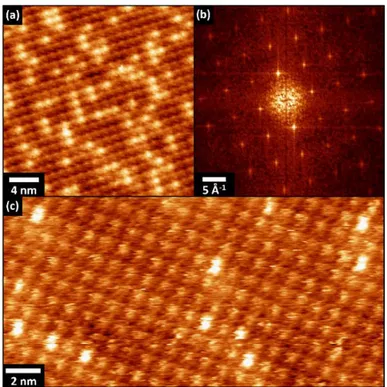
Before deposition of ZnTPP molecules on Au(111), the pristine surface was extensively characterized by STM. Large and small scale STM images of the bare substrate were acquired (for further information see Appendix section, Fig. A1), which exhibit large terraces up to 200 nm separated by monoatomic steps and the typical herringbone (HB) reconstruction with atomic resolution superimposed to it.
In the monolayer regime, ZnTPP molecules form well-ordered and large domains on the Au(111) surface. In particular, three molecular rotational domains were found on the gold surface and each domain, which has the same molecular packing respect to the other two, is rotated of about 30°± 2° relative to one another, as shown in Fig. 2(a). The rotation angle between the domains clearly suggests that these different orientations are due to the 6-fold symmetry of the Au(111) surface.[48]
Figure 2. (a) 85x58 nm2 room temperature STM image depicting three rotational domains of
ZnTPP molecules on Au(111). Tunneling parameters: Ut=1.2 V , It=0.1 nA. (b) Fourier analysis of the
image in (a) that clearly show the presence of the rotational islands.
A representative high-resolution STM image of the ZnTPP molecular packing on Au(111) is shown in Fig. 3. Here the two evident brighter structures, circled by black dashed line, indicate molecules of the second layer, while the other molecules are representative of the first layer.
24
Figure 3. 12x12 nm2 room temperature STM image of ZnTPP on Au(111). Tunneling parameters: Ut
=0.9V, It=0.1 nA. a, b and θ are the unit cell parameters. Inset: FFT analysis of the STM acquisition; A, B
and θ are the lattice parameters in the reciprocal space. The relation between the parameters in the real and reciprocal space is given by A=1/(a*sin θ), B=1/(b*sin θ).
Firstly, the ZnTPP arrangement within the molecular array is discussed. ZnTPP molecules self-assemble in a stable molecular pattern and the measured nearly square unit cell, with lattice parameters a=14.0Å ± 0.1 Å, b= 13.6Å ± . Å a d θ= . °± . °, is comparable with the related literature data.[23,24,26] The resulting molecular density is 0.53 molecules/nm2. These values are
the results of a wide statistical analysis performed on several filtered images, the so-called self- o elated pi tu es, as sho i Fig. .
Figure 4. (a) 20x20 nm2 room temperature STM image of ZnTPP on Au(111). Tunneling parameters: Ut
=0.9V, It=0.1 nA. (b) Filtered (i.e. self-correlated) image of the previous STM picture. The blue and green
lines identify the directions of the unit cell parameters a and b, while the corresponding line profiles are represented in (b1) and (b2), respectively (see the dashed blue and green lines).
25 STM image in Fig. 3 shows ZnTPP molecules slightly darker at the center and with small protrusions at the corners. The faint darker spots, close to the center of the molecules, are related to the position of the Zinc atoms and can be explained, as already reported in literature,[24,26] by considering the electronic configuration of the Zinc ion and the relationship
between its electronic configuration and the tunneling parameters used to acquire the images. In this case, the dark spot at the center of the macrocycle is due to the small contribution to the tunneling current of the Zn atom, which has a filled 3d10 orbital, for a +0.9V
applied bias. The lower tunnel probability of the filled d orbital produces the same effect in other molecular self-assemblies, as NiTPP[25] and metal phthalocyanines.[49,50]
Fig. 3 also exhibits that the internal structure of the porphyrin ring, i.e. the Zn porphyrin macrocycle, is well-defined, while the four meso-phenyl groups can be associated to the protrusions below the ZnTPP core. However, the position of the ZnTPP phenyl groups is not well-defined as in previous literature data.[23,24] Furthermore, the molecules seem to have lost
their typical four-fold structure, i.e. the D4h symmetry (see Fig. 1), after deposition on the
Au(111) surface, which cannot exclude that the molecules could be distorted on the gold surface.
In order to clarify these aspects concerning the molecular packing, a filtered STM image of the ZnTPP molecule is calculated, as shown in Fig. 5 (b). This last picture consists of identical porphyrin molecules, which were obtained by summing several ZnTPP one above the other starting from an acquired image. As a consequence, the noise reduction due to the summing procedure lead to a o e lea shape of the a e aged ole ule. This particular procedure, though unconventional in the STM analysis, is a useful tool in order to explain the molecular packing. Each pyrrolic group can be easily identified on the surface (see the superimposed molecular macrocycles in Fig. 5(b)) and these moieties could be not equivalent on the Au(111) surface. On the contrary, the phenyl groups do not appear so evident and not correspond to the typical position reported in literature[24] (see the red circles in Fig. 5(c)).
26
Figure 5. (a) 6x6 nm2 room temperature STM image of ZnTPP on Au(111). Tunneling parameters:
Ut =0.9V, It=0.1 nA. The ZnTPP macrocycle structure is superimposed on the image. (b)-(c) Filtered
molecular image on which only the ZnTPP macrocycle and the ZnTPP molecular model are superimposed, respectively. The red circles in (c) point out the impossibility to the phenyl groups to be located in the position indicated by the molecular model superimposed on the acquired picture.
By considering the previous STM studies carried out on the ZnTPP deposition on the Au(111) surface,[23,24,26] they suggest that ZnTPP molecules lies flat on the gold substrate, with the
porphyrin macrocycle parallel to the surface. The phenyl groups are instead rotated upon adsorption, which giving rise to the so-called T-shaped stacking, which is the most energetically favorable geometry involving the phenyl groups.[51] NEXAFS studies performed
on similar systems, confirm the rotation of the phenyl groups of TPP molecules adsorbed on metallic surfaces.[30,41,43,52] However, low temperature STM (LT-STM) and NEXAFS studies
performed on other TPP molecules deposited on Au(111) exhibit usually the reduced C2v
symmetry, compared to the four-fold structure (i.e. D4h symmetry) of the free
molecule.[35,39,40,41,44] This reduced symmetry of the porphyrin macrocycle arises from the
molecules-surface bending and leads to the so- alled saddle geo et , hi h is the induced by the adsorption. In this molecular conformation, the porphyrin ring is not flat but alternately pyrrolic units are bent upward and downward relative to the surface. Therefore, the interaction between the core and the metallic surface leads to the deformation of the porphyrin core. Moreover, although not experimentally measured, it can be assumed that the Zn2+ large ion can cause an inherent stress on the porphyrin core, which might lead to a
modified adsorption of the TPP molecule on the surface.[53]
The structural complexity of the ZnTPP molecule, in term of rotational degrees of freedom of the phenyl-groups and flexibility of the porphyrin macrocycle, can complicate the interpretation about the conformational adaptation of the molecule after the adsorption on the gold surface, by using only the STM investigation. In our study, if on one hand the STM
27 experimental results shows a unit cell comparable with the literature data, on the other side the loss of the four-fold symmetry, the unusual position of the phenyl groups as well as the assumed non-equivalence of the pyrrolic moieties not exclude a charge dishomogeneity present at surface, perhaps connected to a distorted ZnTPP molecules on the Au(111) surface. As a consequence, the T-stacking adsorption could not be confirmed in our case. Other information both regarding the adsorption sites of the molecules and the molecular orientation with respect to the high symmetry directions of the Au(111) surface cannot be gained.
However, it is worth noting that the fundamental result of our STM investigation is that the gold herringbone (HB) reconstruction is no longer detected after the ZnTPP deposition (see Fig. 3 in the chapter and also Fig. S2 in the Appendix section). This behavior is not usual considering both the previous works of ZnTPP on Au(111)[23,24,26] rather that other organic
self-assembled monolayer adsorbed on Au(111),[44,54,55] even those in which the molecules show
the saddle geometry.[35] The HB reconstruction is in fact usually observed beneath the adlayer,
when the interaction between the molecules and surface is not strong enough to destroy or lift the electronic properties of the Au(111) surface. Here, as a result, the complete absence of gold HB reconstruction suggests that the interaction between the molecules and surface is not as weak as one could expect from this particular system.
In another study of ZnTPP deposited on Au (111),[24] a relaxing effect of the herringbone was
observed, but the gold superstructure is still revealed. That work reports that the Au(111) surface stress anisotropy between the [̅̅ ] and [ ̅ ] directions is reduced by the ZnTPP molecular adsorbates. In their model, Ruggieri et al.[24] suppose that the anisotropic surface
stress is most likely linked to the inequivalent pyrrole orientation with the result that the pyrrole groups closer to the surface Au atoms exert a force on these atoms, altering the pristine surface energetics. In our work, the total absence of HB reconstruction is instead ascribed to a considerable interaction between the porphyrin core and the gold surface. In other words, after the molecular deposition, a gold surface reorganization occurs. Charge transfer or charge redistribution between the adsorbate and substrate[45] and mechanical
stress applied by the ZnTPP molecules on the Au substrate[56] are the main effects that can
produce the surface reorganization, although they usually are not completely distinguished from each other. As a result, STM investigation shows a ZnTPP molecule considerable interacting with the Au(111) substrate on the Au(111).
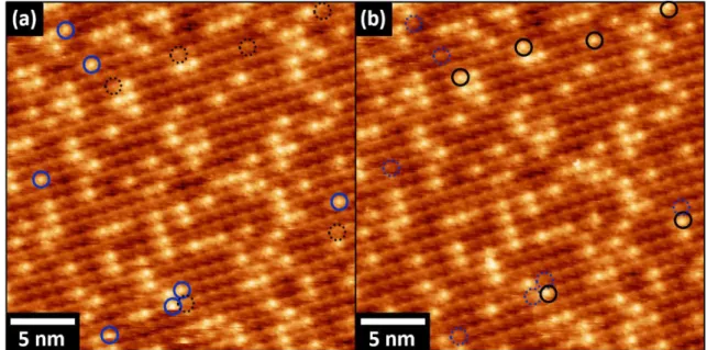
28 In addition, STM investigation allows to gain essential information regarding the partial second layer array of ZnTPP molecules. The STM image and the corresponding FFT analysis, shown respectively in Fig. 6(a)-(b), confirm that the molecular lattice of the incomplete second layer, i.e. the brighter features in the image below, is the same of the first one (i.e. the dark pattern). In particular, the well-defined spots of the Fourier analysis (see Fig. 6(b)) ensure that only one periodicity is present on the surface. In other words, the second layer is organized as the first one. Literature data also suggest that molecules can be absorbed on the Au(111) substrate in a layer-by-layer configuration, at least until the third layer.[23] This last phenomenon that leads
to the formation of stacking layers of ZnTPP is considered a peculiar property of this molecule, in which a particular attractive intermolecular interaction between the stacked molecular plane can be supposed.[26] Furthermore, regarding the reciprocal position between the first
and second layer molecules, STM measures show that the second layer was epitaxially formed on the first ZnTPP monolayer (see Fig. 6(c)). This results is also consistent with the literature data.[26]
Figure 6. (a) 30x30nm2 and (c) 30x15 nm2 room temperature STM images of ZnTTP molecules on gold
surface. The second layer molecules are clearly evidenced by the brighter features. (b) FFT analysis of the previous STM picture. Tunneling parameters: (a) Ut=1.1V, It=0.1 nA; (c) Ut=1 V, It= 0.1 nA.
29 2.3.2 XPS investigation of ZnTPP coverage dependence on Au(111)
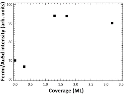
To shed light on the bonding between ZnTPP and Au(111), photoemission experiments on both core-levels and valence band as a function of molecular coverage were performed. In order to understand the adsorption mechanism in the few layers regime, photoemission measurements from sub-monolayer up to about 3 ML thickness are shown, monitoring binding energy shifts and line shape evolution of selected photoemission peaks.
The N1s photoemission peak is very sensitive to the ZnTPP adsorption configuration, as four N atoms are bound both to the central metal atom and the carbon ring skeleton (see Fig. 1), thus revealing any asymmetry in the chemical bond due to the substrate. On the other hand, the thi k molecular film, where van der Waals forces acting between molecules are prevalent with respect to the substrate influence, can be assumed as reference of the ZnTPP gas-phase molecules.
According to the literature, the gas-phase spectrum shows a single symmetric component of the N 1s photoemission peak, centered at about 398.5 eV of binding energy (B.E).[41]
Deviations from the N 1s line shape of the gas-phase molecules can be inferred to chemical interaction and/or structural mismatch with the substrate.[35,41] In particular, the adsorption
of 1ML ZnTPP molecules on the weakly interacting Ag(110) substrate gives a broad N 1s peak with high binding energy tail,[41] which has been fitted with two distinct components
separated by only 0.37 eV. The double component has been ascribed either to a saddle-distortion of the macrocycle or to a breaking of the D4h symmetry of the ZnTPP molecule,
causing different adsorption sites for N atoms on the rectangular substrate. Further, it is worth noting that in metal free porphyrins two well resolved components of equal intensity separated by about 2 eV appear in the N 1s peak. The double-peak structure clearly indicates two types of nitrogen atoms equally distributed, namely aminic (-NH-) and iminic ones (=N-). This interpretation is in line with other photoemission experiments reporting a mixture of metal and metal-free TPP on different substrates, showing the convolution between corresponding components according to the degree of metalation.[57-60]
Fig. 7(a) shows the N 1s photoemission peak as a function of the ZnTPP coverage on Au(111). Starting from the sub-monolayer regime (0.3 ML), the N 1s peak exhibits at least two main components with different intensity ratio. The separation between the two main components is within 2 eV, which is in between the cases above discussed.
30 The main component (see the blue filled in Fig. 7(a)), at lower binding energy, exhibits a forward shift by about 0.5 eV going to lower coverage, reaching 397.8 eV of B.E. at 0.3 ML. According to the literature, the shift of monolayer spectra has been assigned to a final state effect, specifically to an improved polarization screening of the core-hole driven by the substrate. The same shift was here observed for C 1s spectra (see Fig. A3 in Appendix section). By comparing the binding energy related to the gas-phase of ZnTPP molecules, centered at about 398.5 eV,[41] shown by the arrow in Fig.7(a), with that measured at 3.2 ML (i.e. the blue
filled in Fig. 7(a)), we estimate in our system a few-layer regime rather than a multi-layer one. The broader minor component (see the red filled in Fig. 7(a)) at higher B.E. is centered at 399.70 eV ± 0.20 eV regardless of the coverage. Unlike the low binding energy component, which increase with the coverage increasing, this last feature reaches a saturation intensity above 1 ML coverage, as shown in Fig. 7(b). The accuracy of the N 1s intensities analysis is confirmed by the fact that the N1s total intensity is linear with the molecular coverage (see Fig. 7(b).
The chemical shift of the N 1s peak here reported and its evolution with the coverage suggests the coexistence of several different chemical environments of nitrogen atoms within the molecule. We deduce that the minor component is representative of the monolayer (ML) regime and it refers to an inhomogeneous charge distribution, which can be connected to the STM measurements. We point out that compared to Ag(110),[41] the N 1s peak on Au(111)
here reported exhibits a high binding energy component further separated from the main peak, likely indicating either a stronger molecular distortion or a greater charge inhomogeneity. Moreover, the lack of a continuous shift together with a saturated intensity above 1ML suggests that this component is almost restricted to the sub- and monolayer regime.
On the other hand, the main component here detected is likely due to nitrogen atoms in a chemical environment of flat (i.e. free) molecules. Indeed, the configuration of ZnTPP non interacting with the Au(111) substrate is prevalent above 1 ML, where the thick layer film approaches the gas-phase.
31
Figure 7. (a) N 1s photoemission peak as a function of the ZnTPP coverage on Au(111). Two distinct
components are clearly evidenced. All XPS spectra were fitted by using Voigt profile shapes, after Shirley background subtraction. (b) Quantitative N1s intensities of the two component as a function of the molecular coverage.
Additional information can also be obtained by the analysis of the Zn 3d photoemission peak as a function of the ZnTPP coverage on Au(111), as reported in Fig. 8. It is worth noting that, at odd with several studies where a single Zn 3d component has been reported,[61] here the
Zn 3d peak can be fitted by two gaussian components, separated by about 0.9 eV. The chemical shift of Zn 3d here observed can be caused in principle by initial state effects, which are further influenced by relaxation shifts in a lower energy scale (within 0.5 eV).
In the sub-monolayer regime just the low binding energy component, i.e. the red filled in Fig. 8, is observed. This suggests that the low energy feature is essentially due to Zn atoms affected by the Au(111) substrate. As a consequence, in the sub- and monolayer regime Zn atoms have a single environment, due to the concurrent coordination of N atoms and to the interaction with the substrate. This hypothesis is further confirmed by the fact that the intensity of this feature increases more slowly compared to the other component, as coverage increases. Indeed, the second feature at higher B.E., i.e. the blue filled in Fig. 8, appears only above 1ML and keeps on increasing with the second and third layer population, in line with the results above discussed for the N 1s peak. We point out that while the Zn 3d peak exhibits a single
32 component in the sub- and monolayer regime, the N 1s one is instead chemically shifted from the first deposition. This difference most likely indicates that, starting from the submonolayer regime, the four N atoms within the molecule are unequally bound to the substrate.
In summary, the chemical shift of both N 1s and Zn 3d peaks indicates a considerable interaction of ZnTTP molecules on Au(111) in the few-layers regime, supporting as well the charge dishomogeneity revealed by our STM findings.
Figure 8. (a) Zn 3d photoemission peak as a function of the ZnTPP coverage on Au(111). Two distinct
components are clearly evidenced over the ML coverage. All XPS spectra were fitted by using Voigt profile shapes, after Shirley background subtraction. (b) Quantitative Zn 3d intensities of the two component as a function of the molecular coverage. Once again, the accuracy of the Zn 3d intensities analysis is confirmed by the fact that the total intensity of Zn 3d is linear with the molecular coverage (see Fig. 7(b).
In addition, the valence band spectra of clean and ZnTTP-covered Au(111) is reported in Fig. 9(a). Here the coexistence of substrate-related features and molecular overlayer ones can be observed. The clean Au(111) spectrum (see the bottom curve of Fig. 9(a)) exhibits 5d related features in the region between 7 eV to 2 eV, while the Fermi level is mainly due to 6s related states. From an initial analysis of the valence band, it worth noting that the ZnTPP components are not well resolved due to their overlapping with gold ones. In fact, the only component which is strictly discernible is the Zn 3d photoemission peak, ranging from 10 eV to 11 eV.