Annealing kinetics of vacancy-related defects in low-dose MeV self-ion-implanted n-type silicon
P. Pellegrino, P. Le´veˆque, J. Lalita, and A. Halle´nRoyal Institute of Technology, Solid State Electronics, P.O. Box E229, SE-164 40 Kista-Stockholm, Sweden C. Jagadish
Australian National University, Department of Electronic Materials Engineering, Research School of Physical Sciences and Engineering, Canberra ACT 0200, Australia
B. G. Svensson
University of Oslo, Physics Department, Physical Electronics, P.B. 1048 Blindern, N-0316 Oslo, Norway and Royal Institute of Technology, Solid State Electronics, P.O. Box E229, SE-164 40 Kista-Stockholm, Sweden
共Received 26 March 2001; published 30 October 2001兲
Silicon samples of n-type have been implanted at room temperature with 5.6-MeV28Si ions to a dose of 2⫻108cm⫺2and then annealed at temperatures from 100 to 380 °C. Both isothermal and isochronal treatments were performed and the annealing kinetics of the prominent divacancy (V2) and vacancy-oxygen共VO兲 centers were studied in detail using deep-level transient spectroscopy. The decrease of V2centers exhibits first-order kinetics in both Czochralski-grown共CZ兲 and float-zone 共FZ兲 samples, and the data provide strong evidence for a process involving migration of V2 and subsequent annihilation at trapping centers. The migration energy extracted for V2 is ⬃1.3 eV and from the shape of the concentration versus depth profiles, an effective diffusion length⭐0.1 m is obtained. The VO center displays a more complex annealing behavior where interaction with mobile hydrogen 共H兲 plays a key role through the formation of VOH and VOH2centers. Another contribution is migration of VO and trapping by interstitial oxygen atoms in the silicon lattice, giving rise to vacancy-dioxygen pairs. An activation energy of⬃1.8 eV is deduced for the migration of VO, in close resemblance with results from previous studies using electron-irradiated samples. A model for the annealing of VO, involving only three reactions, is put forward and shown to yield a close quantitative agreement with the experimental data for both CZ and FZ samples over the whole temperature range studied.
DOI: 10.1103/PhysRevB.64.195211 PACS number共s兲: 61.80.Jh, 71.55.⫺i, 85.40.Hp I. INTRODUCTION
It is well established by several fundamental studies that MeV electron irradiation and ion implantation of silicon give rise to similar kinds of point defects, although the relative importance of the different defects hinges on the projectile mass; for a recent review see Ref. 1. This similarity holds if the ion dose is kept below a critical value, which is closely associated with the ion mass and energy. In this ‘‘low-dose’’ regime single collision cascades prevail and the overlap be-tween different ion tracks is small. Hence, agglomeration phenomena, which can lead to the formation of extended clusters and eventually to complete amorphization, are to a large extent suppressed. The main difference between the damage introduced by energetic electrons and ions is, how-ever, to be found in the spatial distribution of the defects. In contrast to MeV electron irradiation, ion implantation gives rise to a localized damage distribution, with a peak region close to the projected ion range and a tail towards the sur-face. Because of a high concentration of defects, the strain field at the end of the ion range can suppress the capture of free charge carriers by electrically active defects, as well as affect the atomic- and electronic-defect configurations.2 Fur-thermore, the flux of the diffusing defects is expected to be influenced by the concentration gradient in the peak region. For MeV electron irradiation the kinetics of point-defect generation has been studied by different groups,3– 8and to-day, there is a reasonable understanding of the defect
reac-tions taking place in an irradiated layer. In this respect, it has been crucial to reveal the presence of different impurity at-oms in the starting material, e.g., oxygen, carbon, hydrogen, and dopant atoms共phosphorus, in our case兲. Their role is to act as traps for the mobile vacancies and interstitials, com-peting strongly in the promotion or suppression of stable complexes.
However, for ion implantation only a few quantitative studies of the point-defect generation exist,9–13 and the de-fects primarily investigated are the divacancy (V2) and vacancy-oxygen 共VO兲 centers. V2 and VO are the most prominent vacancy-related defects in silicon after low-dose ion bombardment at room temperature共RT兲 and their forma-tion has been studied as a funcforma-tion of ion mass, dose, dose rate, sample depth, and implantation temperature. At dose rates below⬃108cm⫺2s⫺1, the generation of V2centers per ion-induced vacancy in the damage peak region is identical, within⫾10%, for different kinds of ions ranging from11B to 120Sn共this may hold for an even wider range of ions but to the best of our knowledge no such data exist in the litera-ture兲. In contrast, the VO center shows a decrease in the generation rate per ion-induced vacancy with increasing ion mass, consistent with the picture from molecular-dynamics simulations suggesting that light ions are more effective than heavy ions in generating point defects.14 The concentration of both V2and VO increases linearly with the ion dose in the regime where single-collision cascades prevail (⭐1010cm⫺2), but the generation efficiency per ion
de-sociate, migrate to annihilation sinks, interact with each other or with impurities, etc. Given the quite large choice of possible simultaneous reactions, it is important to consider carefully all the factors involved, such as the aforementioned spatial distribution of defects and the impurity content. In some cases, as for the annealing of the vacancy-phosphorus center, a dependence on doping concentration, illumination, and electric field has also to be taken into account.17,18
Quantitative studies of the annealing kinetics for the V2 and VO centers have mainly been performed using electron-irradiated samples and employing infrared spectroscopy共IR兲 or, to some extent, deep-level transient spectroscopy共DLTS兲 for the analysis.3,19–22Despite their fundamental importance, quantitative annealing data for V2 and VO in ion-implanted samples are scarce. A particular requirement for the latter type of samples is the necessity to determine concentration versus depth profiles because of the non-uniform defect gen-eration. This limits the applicability of IR spectroscopy for implanted samples and favors the use of DLTS. Hence, the defect concentration must be kept low, typically⭐1014cm⫺3 for a doping concentration of ⬃1015cm⫺3, which is about three to four orders of magnitude below that normally used in IR studies (⬃1017– 1018cm⫺3).
In this work the annealing kinetics for the V2 and VO centers are quantitatively determined in MeV self-ion-implanted Czochralski-grown 共CZ兲 and float-zone 共FZ兲
n-type silicon samples using DLTS. The annealing of V2 follows first-order kinetics and is attributed to migration of the V2 centers before trapping by immobile defects/ impurities. The loss of VO displays a more complex behav-ior, which can be partly described by passivation through reaction with mobile hydrogen atoms originating from a thin surface layer. The passivation is modeled by a two-stage pro-cess, where first the VOH center appears, being electrically active and possible to monitor by DLTS,23before the electri-cally neutral VOH2center is formed. A competing reaction, effective at temperatures ⭓300 °C, is the migration of VO centers and subsequent formation of vacancy-dioxygen pairs (VO2) via trapping by interstitial oxygen atoms (Oi) in the silicon lattice. A close agreement between the experimental data and computer simulations of the annealing kinetics is reached for VO using a model involving only three reactions.
II. EXPERIMENT
N-type共关Ps兴⫽9⫻1014cm⫺3, where brackets denote con-centration values and subscript s refers to substitutional
lat-Circular diode areas, with a diameter of 2.5 mm, were pat-terned and etched in a buffered hydrofluoric共HF兲 solution. A screen oxide, with a thickness of 200 Å, was grown prior to the p⫹ implantation of 50-keV boron ions with a dose of 5
⫻1015cm⫺2. The samples were then implanted on the back-side with 1⫻1015P/cm2共80 keV兲, ensuring a good Ohmic contact. Subsequently, annealing was carried out at 1000 °C for 40 min, in order to activate the implanted dopants. Con-tact holes were defined by means of lift-off lithography, and aluminum was deposited on the front and backside of the samples followed by annealing at 450 °C for 30 min in argon atmosphere. Together with the CZ samples, these p⫹n
di-odes were then implanted at RT with 5.6-MeV Si⫹ions using the Uppsala EN tandem accelerator.24 The implantation en-ergy was chosen to generate a defect distribution suitable for monitoring by DLTS, and the damage peak was located⬃3.6
m below the surface. The ion dose (2⫻108cm2) was tuned to avoid doping-compensation effects, and the error in the nominal dose did not exceed 15%.
Subsequently, Schottky-barrier junctions were prepared on the CZ samples. Following a standard cleaning process, which includes a final dip in diluted HF solution共10%兲, ther-mal evaporation of Au contacts was performed at a pressure of ⬃1⫻10⫺6mbar. The temperature of the samples during contact growth did not exceed 50 °C.
Isochronal and isothermal anneals of both types of samples were performed in nitrogen atmosphere at tempera-tures between 100 and 380 °C. DLTS analysis was then car-ried out using a refined version of the setup described in Ref. 25. Up to nine different spectra, each of them corresponding to a particular time window, could be recorded simulta-neously. In this way, the measurement time was minimized and a high-energy resolution was achieved when character-izing the deep levels observed. A filling pulse of 10 ms du-ration was applied, ensuring that even traps with small cap-ture cross sections, of the order of 10⫺18– 10⫺19cm2, were fully saturated and contributed to the recorded emission. Fur-ther, capture-cross-section measurements were undertaken by variation of the filling pulse width.
Concentration versus depth profiles of the defect levels were obtained by selecting one rate window and holding the temperature constant at the maximum of the DLTS peak of interest. The steady-state reverse-bias voltage was kept con-stant while gradually increasing the amplitude of the filling pulse. The depth profiles were then extracted from the de-pendence of the recorded DLTS signal on the pulse amplitude,5 where the voltages used were converted into
depth according to the conventional square-root dependence for a Schottky-barrier or pn junction.
III. RESULTS
Figure 1 shows DLTS temperature scans after isochronal
共30 min兲 annealing of implanted CZ samples. The
character-istic peaks primarily attributed to the VO center at EC
⫺0.17 eV and to the doubly and singly negative charge
states of V2 at EC⫺0.23 eV and EC⫺0.42 eV, respectively, are identified3,5,20,26 –31 共EC denotes the conduction-band edge兲. These two centers dominate the majority carrier spec-trum for n-type samples and are normally the prime defects after implantation at low doses, together with the interstitial-carbon–interstitial-oxygen complex (CiOi) having a level at
⬃0.35 eV above the valence-band edge7,32,33 共not shown here兲. The apparent deviation from a 1:1 ratio between the singly negative (V2⫺) and doubly negative charge state (V22⫺) of V2 is a characteristic feature of ion bombardment,9,34together with a highly nonexponential cap-ture rate of the EC⫺0.23 eV level as a function of the filling-pulse duration.2 Both phenomena are enhanced as the mass of the impinging ions increases and can be regarded as two different aspects of the suppression of V22⫺ in the damage peak region, as has been discussed in detail in Refs. 2, 9, and 34.
It is well established that the EC⫺0.42 eV peak contains contributions also from the vacancy-phosphorus 共VP兲 center30,35 and possibly from the interstitial-carbon– substitutional-phosphorus (CiPs) complex.
36 –39
Even if it is difficult to directly resolve the contributions of these addi-tional defects by means of convenaddi-tional DLTS their thermal stability is less than that of V2.17,35Both VP and CiPs disap-pear rapidly at 150 °C and as shown in Fig. 1, the amplitude of the EC⫺0.42 eV peak decreases by ⬃10% after 30 min, consistent with the magnitude expected for these centers in moderately doped (关Ps兴⬃1015cm⫺3) CZ samples.38 It may be noted that the peak shifts to slightly higher temperatures after annealing, in accordance with a somewhat higher rate of electron emission from VP than V2⫺ at a given
temperature.40 Moreover, at 150 °C a small level at EC
⫺0.36 eV disappears. This level was also found in the FZ p⫹/n samples and investigated after reverse-bias cooling or minority-carrier injection. The behavior and thermal stability of the EC⫺0.36 eV level resemble closely those of one
共metastable兲 state of the CiPs complex, studied in detail for electron-irradiated samples.36 –39 关EC⫺0.36 eV兴 is quite small (⬍1013cm⫺3), as expected with 关Ps兴⬇1
⫻1015cm⫺3, and does not affect the stability of VO and V 2. Further, it was verified that the concentration of the substitutional-carbon–interstitial-carbon pair (CsCi) is negli-gible in both sets of samples at any stage of the annealing experiments. The DLTS signal of CsCi overlaps strongly with that of VO, but its presence can be readily resolved by variation of the filling-pulse width.2
As shown in Fig. 1, annealing of the CZ samples at and above 200 °C results in a progressive reduction in the con-centration of both V2 and VO. The concentration of V2 is below the detection limit at 300 °C, while VO still persists at temperatures well above 300 °C. At this stage small signals originating from levels at about EC⫺0.20 eV and EC
⫺0.59 eV are detected. There is scarce information in the
literature regarding these two levels, and their small intensi-ties preclude any accurate characterization. We could not es-tablish any correlation between their presence and the an-nealing of V2 and VO, but it is worth mentioning that they appear simultaneously with the growth of a level at EC
⫺0.32 eV. This latter level originates from a defect already
present in small concentration directly after implantation in the CZ samples and which then gradually increases with an-nealing up to 300 °C. In accordance with previous notations,9,41we label this level as E3.
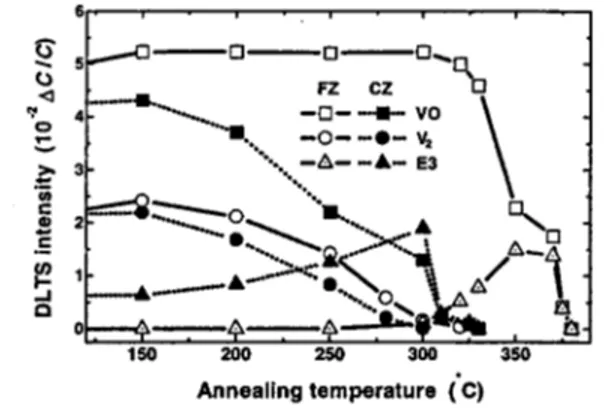
A similar isochronal annealing study for the FZ samples yields different results compared to those in Fig. 1. As illus-trated in Fig. 2, an overall higher thermal stability of the defects is observed, especially for the VO center. The anneal-ing of V2 and VO take place in two distinctly different tem-perature regimes, and moreover, E3 is not detected until temperatures where VO starts to disappear. It may also be noted that even at the lowest temperature 共150 °C兲 in Fig. 2
关VO兴 is larger in the FZ samples, despite two orders of
mag-FIG. 1. DLTS spectra of CZ n-type Si samples after isochronal
共30 min兲 annealing between 150 and 300 °C. The samples were
implanted at RT with 5.6-MeV silicon ions to a dose of 2
⫻108
cm⫺2. The emission rate at the peak maximum is 7.5 Hz.
FIG. 2. DLTS signals of the levels at EC⫺0.17, EC⫺0.23, and
EC⫺0.32 eV, corresponding to VO, V2, and E3, respectively, after
isochronal共30 min兲 annealing between 150 and 380 °C. Results for both CZ and FZ samples are included.
nitude lower concentration of interstitial oxygen relative to that in the CZ samples. However, the sum关VO兴 and 关E3兴 is identical in the two materials at 150 °C, providing further indication that the loss of VO is correlated with the growth of E3, as will be discussed in detail in Sec. IV B. Moreover, the identical sum of 关VO兴 and 关E3兴 in the two materials implies that an oxygen concentration in the low 1015cm⫺3 range is sufficient to efficiently trap migrating monovacan-cies that have escaped recombination or higher-order defect formation in the collision cascades. For the ion dose used in this work (2⫻108Si ions/cm2) the peak concentration of monovacancies surviving annihilation is estimated to be in the low 1013cm⫺3range.11
By performing isothermal treatments of the CZ and FZ samples in the 190–260 °C temperature range, the annealing kinetics of V2 has been explored. In the whole interval an exponential decrease as a function of annealing time holds with a high accuracy, Fig. 3. The integrated intensity of
关V2(x,t)兴 after each annealing step can be expressed by
冕
关V2共x,t兲兴dx⫽冕
关V2共x,t⫽0兲兴dx exp关⫺c共T兲t兴, 共1兲 where x is the sample depth and t is the annealing time, i.e., the process follows first-order kinetics with a temperature-dependent rate constant c(T). As shown in Fig. 4, c(T) ex-hibits an Arrhenius dependence,c共T兲⫽c0exp共⫺Ea/kT兲, 共2兲
where c0 and Ea are the frequency factor and the activation energy, respectively. k is Boltzmann’s constant and T is the absolute temperature. The values of c(T) obtained for the CZ samples are about a factor of 2 higher than those for the FZ samples, and the extracted values for c0 and Ea are⬃1
⫻109(⬃5⫻108) s⫺1and 1.27⫾0.04 (1.25⫾0.05) eV in the CZ共FZ兲 samples, respectively. No electrically active defects have been detected with a growth correlated to the loss of
V2. This is true even for shallow energy levels extending the temperature range of the DLTS measurements to below 30 K where the phosphorus donor starts to freeze out.
In Figs. 2– 4, the V2 center is represented by the EC
⫺0.23 eV level (V2 2⫺
) but well within the experimental ac-curacy of the data; the EC⫺0.42 eV level (V2⫺) displays the same annealing rate. In this context it should be emphasized that no broadening of the concentration versus depth profiles of V2 is revealed during the annealing. The profile shape remains the same except for an initial narrowing around the peak region after the first annealing step at each temperature. A similar behavior is also observed for the VO center and the narrowing is due to a decrease of the tail towards the surface. This has been discussed in detail previously42 and the nar-rowing exhibits a transient behavior with no temperature de-pendence in the studied range 共100–380 °C兲. Consequently, for the annealing kinetics the depth distributions of V2 and VO can be considered as invariant. In the following,关V2(t)兴 and关VO(t)兴 will denote 兰关V2(x,t)兴dx and 兰关VO(x,t)兴dx, respectively.
Analogous isothermal annealing as for V2was performed for the VO center. As already demonstrated, substantially higher temperatures are required in order to affect the stabil-ity of VO in the FZ samples than in the CZ samples. Apart from this important difference, the annealing of VO displays similar features in the two materials. As illustrated in Fig. 5 for the CZ samples, at each annealing temperature two dif-ferent stages can be identified, a fast initial process followed by a considerably slower one. An analytical expression to fully describe the annealing of VO in the whole temperature range studied has not been found. It is apparent from Fig. 5 that a composition of two first-order processes, which would result in two linear regions, is not adequate for all the tem-peratures. Furthermore, the rate of the initial drop increases with关VO(t⫽0)兴, as revealed by the inset in Fig. 5, compar-ing results of samples implanted with 1⫻108 and 2
⫻108ions/cm2.
If a second-order process is put forward, then 关VO(t)兴 should evolve according to
d关VO共t兲兴/dt⫽⫺K共T兲关VO共t兲兴2, 共3兲
where K(T) is a second-order rate constant. In this case the annealing rate depends on 关VO(t⫽0)兴, as one finds by in-tegrating Eq.共3兲,
FIG. 3. Integrated intensity of 关V2(x,t)兴 共EC⫺0.23 eV level兲 after isothermal annealing of CZ samples at temperatures between 190 and 260 °C. The intensity has been normalized to that in as-implanted samples. The solid lines represent a least-squares fit of the experimental data.
FIG. 4. Arrhenius plot of the rate constant c(T) for annealing of
关VO共t兲兴⫽关VO共t⫽0兲兴/关1⫹␣共T兲t兴, 共4兲
where␣(T)⫽关VO(t⫽0)兴K(T). As shown in Fig. 6 for the FZ samples, Eq. 共4兲 reproduces the experimental data for some temperatures but, in general, it is not satisfactory when the full evolution is considered. This is further substantiated by an even poorer agreement for the CZ samples and more-over, for a second-order process the shape of the distribution
关VO(x,t)兴 should not remain invariant during annealing.
Hence, unlike that for V2, a first-order annealing process can be ruled out for VO and also a second-order process is not appropriate. This suggests a more complex scenario and quite interestingly, a close correlation is found between the decrease of关VO(t)兴 and the evolution of 关E3(t)兴, irrespec-tive of sample characteristics and annealing temperature. In particular, the pronounced reduction in the annealing rate of VO after the initial stage is always accompanied by an onset of saturation in the growth of E3. In Fig. 7, the loss of
关VO(t)兴 and the growth of 关E3(t)兴 are compared as a
func-tion of annealing time at 190, 220, and 250 °C for the CZ samples. In the accessible time scale the annealing process can be decomposed into three different stages. First, a pro-portionality holds between the increase of 关E3(t)兴 and the decrease of 关VO(t)兴, as demonstrated in Fig. 7共a兲 for 190 °C. After a certain time共⬃400 min at 190 °C兲, 关E3(t)兴
and 关VO(t)兴 become comparable and in the second stage,
关E3(t)兴 saturates while simultaneously the decrease of 关VO(t)兴 slows down. The second regime is even more
clearly observed, after the initial short stage, at the interme-diate temperature 共220 °C兲, Fig. 7共b兲. Finally, E3 starts to anneal out with about the same rate as VO. This third stage is readily observed at 250 °C, Fig. 7共c兲.
In the FZ samples the annealing kinetics for VO shows the same trend as in the CZ samples but at substantially higher temperatures. As mentioned previously, in the FZ samples E3 is not detected until temperatures ⭓300 °C. All the three annealing stages can be found in Fig. 8 showing results after isothermal treatment at 330 °C. The first stage occurs for t⭐150 min followed by a saturation in the growth of 关E3(t)兴 and a decrease in the loss of 关VO(t)兴 共second stage兲 before both centers decrease simultaneously for t
⭓400 min 共third stage兲. Analogous results are obtained at all
the temperatures explored for isothermal annealing of VO in the FZ samples共300–380 °C兲.
IV. DISCUSSION A. V2center
The annealing of V2 is established to follow first-order reaction kinetics, irrespective of FZ or CZ samples. Further, FIG. 5. Integrated intensity of 关VO(x,t)兴 共EC⫺0.17 eV level兲
after isothermal annealing of CZ samples at temperatures between 190 and 260 °C. The intensity has been normalized to that in as-implanted samples. The inset compares the initial loss at 260 °C between two samples implanted with a dose of ⬃1⫻108cm2
共sample no. 1兲 and 2⫻108cm⫺2共sample no. 2兲, respectively.
FIG. 6. Reciprocal of the integrated intensity of 关VO(x,t)兴 (EC⫺0.17 eV level兲 in FZ samples after isothermal annealing at temperatures between 300 and 370 °C. The values have been nor-malized to that in as-implanted samples. For second-order kinetics, a linear dependence on annealing time is expected.
FIG. 7. Evolution of the integrated intensities
of 关VO(x,t)兴 (EC⫺0.17 eV level兲 and
关VOH(x,t)兴 共EC⫺0.32 eV level兲 in CZ samples versus annealing time at 190, 220, and 250 °C. The intensities are compared with those at t⫽0 and the absolute values of the difference are de-picted.
in the FZ samples the loss of V2 and VO take place in two well-separated temperature regimes, and as shown in Ref. 42, the progressive decrease of关V2(x,t)兴 in the 200–250 °C interval occurs without any noticeable change in the concen-tration of VO centers. This implies that the annealing of V2 cannot be ascribed to a flux of silicon self-interstitials anni-hilating vacancy-type centers since it would simultaneously affect 关VO(x,t)兴, which is of the same magnitude as
关V2(x,t)兴. Moreover, dissociation of V2 can be ruled out as a dominant process since it would increase 关VO(x,t)兴, as observed in the case of dissociation of VP.43 In addition, the frequency factors obtained are in the 108– 109s⫺1range共Fig. 4兲, which is a factor of 104– 105 lower than expected if dis-sociation prevails (1012– 1013s⫺1).44 This suggests strongly that the annealing is predominantly controlled by migration of V2 and subsequent annihilation at trapping centers. In or-der to fulfill the first-oror-der kinetics, the concentration of traps must be at least one order of magnitude higher than that of
V2, i.e.,⭓1015cm⫺3.
However, no broadening of the original V2 depth profile, which would be a direct evidence for migration, was de-tected at any stage of the study. This holds even for the FZ samples, having a low concentration of impurities/traps, and in order to make a proper interpretation, quantitative esti-mates based on the observed annealing kinetics are required. The activation energy Eais regarded as the migration energy of V2 共involving partial dissociation兲, while the frequency factor c0 is related to the number of jumps before V2 is captured. The values extracted from the experiments are in accordance with the proposed model. Ea being independent on the material quality while c0is smaller in the FZ samples, as expected for a material with a low concentration of traps. If the total concentration of traps for V2 is denoted by关Z兴, the following relation can be derived by applying the theory for diffusion-limited reactions:45
关V2共x,t兲兴 t ⫽⫺4RDV2关V2共x,t兲兴关Z兴⫹DV2 2关V 2共x,t兲兴 x2 , 共5a兲
where R is a capture radius for the trapping reaction and DV2 is the diffusion constant of V2. Z is considered to be
immo-bile and to have a uniform depth distribution. The first term on the right-hand side of Eq. 共5a兲 accounts for the loss of
关V2兴 and we can write
关V2共x,t兲兴
t ⫽⫺c共T兲关V2共x,t兲兴⫹DV2 2关V
2共x,t兲兴
x2 共5b兲
with c(T) given by Eq.共2兲 and putting c0⫽4RDV2 0
关Z兴 and DV
2⫽DV2
0 exp(⫺E
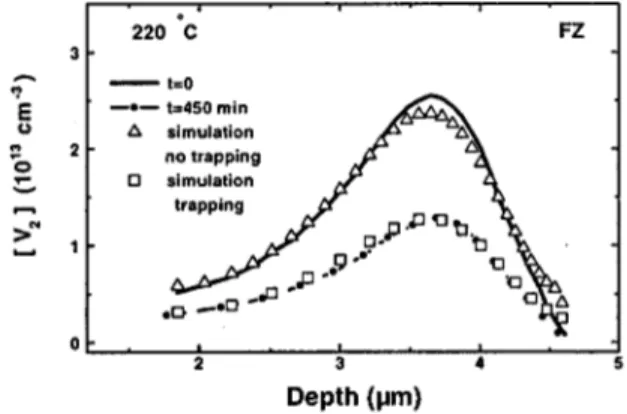
a/kT). R is put equal to 5 Å and Eq.共5b兲 is solved numerically with关V2(x,t⫽0)兴 and c(T) taken from the experimental data. The evolution of 关V2(x,t)兴 is then compared with the measured profiles as a function of anneal-ing time and temperature, and Fig. 9 shows the results共both with and without trapping兲 for FZ samples after 450 min at 220 °C. In order to reproduce the lack of broadening of the
V2 profile, DV2 has to be low. In fact, the effective diffusion length must be smaller than the accessible depth resolution
共⬃0.1 m兲, and the comparison between experimental and simulated data gives a maximum value of ⬃10⫺1cm2/s for
DV2 0
. This value is in the anticipated range and differs less than a factor of ⬃30 compared to the preexponential factor estimated for migration of the monovacancy assuming a small migration entropy (⬃0 k), as expected in the studied temperature range.46
Hence, DV
2
0 ⭐10⫺1
cm2/s implies 关Z兴⭓4⫻1015cm⫺3 in the FZ samples and 关Z兴⭓8⫻1015cm⫺3in the CZ samples, which may be regarded as reasonable lower limits. In addi-tion, these values are fully consistent with the trap concen-trations required for the first-order kinetics to apply. The identity of Z is not known but it should be emphasized that Oican be ruled out as a main candidate; the c0values for the FZ and CZ samples differ only by a factor of 2 while 关Oi兴 differs by at least two orders of magnitude共⭐5⫻1015versus
⬃5⫻1017cm⫺3兲. A more likely candidate is a carbon-related trap since carbon can be present with comparable concentra-tions in FZ and CZ samples. However, no correlation was found between the loss of V2 and the growth of any electri-cally active center. In fact, this provides additional support FIG. 8. Integrated intensity of 关VO(x,t)兴 共EC⫺0.17 eV level兲
and关VOH(x,t)兴 共EC⫺0.32 eV level兲 versus annealing time in a FZ
p⫹n samples annealed at 330 °C.
FIG. 9. Comparison between experimental and simulated con-centration versus depth profiles of V2 共EC⫺0.23 eV level兲 in FZ samples after annealing at 220 °C. For the simulated profiles, Eq.
for the conclusion that Oi can be excluded as a prime trap since V2O (V2⫹Oi→V2O) is expected to be electrically active.30,47,48
The values deduced for c(T) are in close agreement with those obtained from previous studies on electron-irradiated samples, and the same holds for the proposed annealing mechanism. Indeed, a migration energy in the range of 1.25– 1.30 eV has been found by studying reorientation of V2 un-der uniaxial stress using electron paramagnetic resonance3or photoconductivity.49 Slightly higher values for Ea and c0 than those obtained in the present work were extracted from samples irradiated with MeV electrons to high doses (1018cm⫺2) and analyzed by FTIR.22 In Ref. 22, 关V2(x,t
⫽0)兴 is in the range of 1016cm⫺3 and approaches the con-centration of traps. As a result, at long enough annealing times the dissociation rate of V2 becomes comparable with the loss through migration and subsequent trapping. Since both processes can be approximated by first-order kinetics, Eq.共1兲 is still applicable and the extracted values represent a mixed annealing regime. In fact, two individual contributions were deduced yielding an activation energy of⬃1.28 eV for migration and⬃1.7 eV for dissociation.22
B. VO center
The annealing kinetics of VO shows clearly that it cannot be described by a single dissociation or migration/trapping mechanism. In both sets of samples the concentration versus depth profiles of VO exhibit no broadening after thermal treatment.42 Another key result is that the decrease in
关VO(t)兴 is followed by an evolution of the E3 defect 共Ec
⫺0.32 eV level兲. Furthermore, VO displays an increased
sta-bility in the FZ samples relative to that in the CZ samples, with a corresponding inhibition of the appearance of E3.
The exact identification of the E3 center has been a sub-ject of speculation for some time. In one of the first reports,25 it was assigned to a migrating impurity from the surface, coupling with a primary defect introduced by electron irra-diation. Moreover, the hypothesis that VO was the affected defect was put forward, since the production rate of E3 was comparable with that of VO. DLTS experiments after proton implantation41,50 or hydrogenation51 revealed a defect level with the same emission rate as the Ec⫺0.32 eV level, lead-ing to the firm conclusion that hydrogen is one of the con-stituents of E3. More recent studies have finally agreed on the assignment of E3 as a VOH complex.23,52–54In this study we provide additional evidence for this identification, based on the annealing kinetics for VO and E3.
In fact, hydrogen diffusion from the surface is anticipated to take place in the investigated samples. Initially, a signifi-cant amount of hydrogen is confined to the surface region, resulting from the cleaning steps in the diode manufacturing. Because of the high mobility and reactivity of hydrogen, a progressive aggregation with irradiation-induced defects oc-curs even at RT.55Hydrogen is known to modify the electri-cal properties of point defects and ultimately, full passivation may occur. By means of DLTS, it is possible to follow the evolution of these phenomena, e.g., the transformation of VO to VOH. In the case of electron irradiation, the in-diffusing
hydrogen faces a uniform defect distribution51,53 and ini-tially, the depth profile of the VOH centers formed shows a diffusion-like shape from the surface. At later annealing stages, while the hydrogen front advances into the bulk, pas-sivation of the VOH centers occurs in the near-surface region and neutral VOH2centers form. These reactions can be ob-served until the electrically active defects in the explored region are fully saturated, or the supply of free hydrogen is exhausted.
In ion-implanted samples the defects are mostly confined to the peak region, and a somewhat more complex scenario appears than in electron-irradiated samples since the diffus-ing hydrogen reacts with a nonuniform distribution of de-fects. It may be noted that even without intentionally intro-ducing hydrogen, its initial surface concentration is large enough to affect the defect production/annealing in the low-dose regime studied. In order to quantitatively validate this interpretation of our DLTS data, a comparison is made with computer simulations of the annealing kinetics assuming the following reactions:
VO⫹H↔VOH
VO⫹Oi→VO2
VOH⫹H→VOH2
共6兲
where the first reaction represents the formation and disso-ciation of VOH, the second one formation of VO2pairs, and the third one formation of VOH2 centers. Both VO2 and VOH2 are electrically inactive. The capture radius R is put equal to 5 Å, and only hydrogen and VO are considered to be mobile. The set of differential rate equations corresponding to Eq. 共6兲, derived from the theory for diffusion-limited reactions,45 is listed in Table I.
The numerical values used for the hydrogen diffusion co-efficient are given by DH⫽5⫻10⫺3exp关⫺0.8 (eV)/kT兴 TABLE I. Set of simultaneous differential rate equations derived from the reactions in Eq.共6兲. See text for explanation of the sym-bols used. K1⫽4R(DH⫹DVO), K2⫽4RDVO, K3⫽4RDH. In the CZ samples,⌰BH⫽0. 关VO共x,t兲兴 t ⫽DVO 2关VO兴 x2 ⫺K1关VO兴关H兴 ⫺K2关VO兴关Oi兴⫹VOH关VOH兴 关VOH共x,t兲兴 t ⫽K1关VO兴关H兴⫺K3关VOH兴关H兴⫺VOH关VOH兴 关VOH2共x,t兲兴 t ⫽K3关VOH兴关H兴 关VO2共x,t兲兴 t ⫽K2关VO兴关Oi兴 关Oi共x,t兲兴 t ⫽⫺K2关VO兴关Oi兴 关H共x,t兲兴 t ⫽⌰BH⫹DH 2关H兴 x2 ⫺K1关VO兴关H兴 ⫺K3关VOH兴关H兴⫹VOH关VOH兴
cm2/s and are almost identical with those proposed by Rizk
et al.56for diffusion of negatively charged hydrogen (H⫺) in
n-type silicon. Here, it should be pointed out that a quite
large interval exists in the literature regarding the activation-energy values for hydrogen diffusion, ranging from 0.48 eV at high temperatures57 to 1.2 eV at 225–350 °C,58 presum-ably reflecting a strong dependence of the mobility on the hydrogen charge state. It may also be mentioned that an ac-tivation energy of ⬃0.8 eV has been deduced for the diffu-sion of H2 complexes but the pre-exponential factor is only of the order of a few times 10⫺4cm2/s.59,60For the diffusion constant of VO, a value of DVO⫽6 exp
关⫺1.8 (eV)/kT兴 cm2/s is employed, which agrees closely with previous values extracted from FTIR studies of electron-irradiated samples.21,61 The dissociation rate for
VOH is set to VOH⫽5⫻1012exp关⫺1.9 (eV)/
kT兴 s⫺1. A frequency factor of this order is typical for a pure dissociation process, and the activation energy of 1.9 eV is consistent with the thermal stability of the E3 center.
The 关VO(x,t⫽0)兴 profile and a uniform interstitial oxy-gen concentration of 关Oi兴⫽5⫻1017cm⫺3, as determined by FTIR for the CZ samples, were used as input for the simu-lations. The initial hydrogen concentration was put to 4.5
⫻1014cm⫺3 and confined to a 0.2-m-thick surface layer, i.e., 关H(x⭐0.2m,t⫽0)兴⫽4.5⫻1014cm⫺3 and 关H(x
⬎0.2m,t⫽0)兴⫽0. This value is in accordance with the surface concentration of hydrogen on HF cleaned p-type Si wafers, as observed by deactivation of boron acceptors using surface-charge profiling.62Further, it is considerably smaller than that found after intentional hydrogenation processing, which lead to a hydrogen incorporation of the order of 1016cm⫺3in the bulk63 or 1018cm⫺3at the surface.64
Results for two CZ samples annealed at 220 and 250 °C are shown in Fig. 10, and close quantitative agreement with the experimental data is obtained. Moreover, the assumption of an initial surface concentration of hydrogen is strongly supported by the evolution of the 关VO(x,t)兴 and
关VOH(x,t)兴 profiles during annealing. The transient
reduc-tion of the original关VO(x,t)兴 profile towards the surface42is
associated with a concurrent drastic change in the shape of the 关VOH(x,t)兴 profile, starting from a broad distribution and ending with a peaked profile resembling that of VO in as-implanted samples. These important features are repro-duced by the proposed model, as illustrated for VOH in Fig. 11.
In the p⫹/n FZ samples, the incorporation of hydrogen from the surface is retarded by trapping at the boron accep-tors in the p⫹ layer. For instance, atomic hydrogen and the boron acceptor form readily a complex with an estimated dissociation energy in excess of 1.3 eV.65Thus, the p⫹layer acts as an efficient diffusion barrier for hydrogen, explaining the high temperatures needed to observe the interaction be-tween H and VO in the p⫹/n FZ samples. In the simulations, this is taken into account by introducing a thermally acti-vated injection rate of hydrogen from the p⫹layer into the n region, ⌰BH⫽5⫻1012exp关⫺2 (eV)/kT兴 s⫺1. Otherwise, the parameter values used are the same as for the CZ samples, except for a lower oxygen concentration, 关Oi兴⫽2
⫻1015cm⫺3.
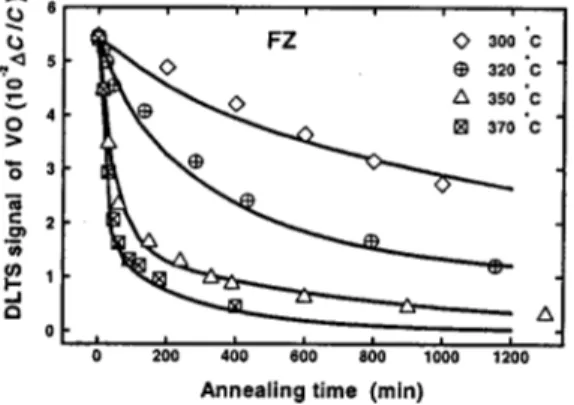
In Fig. 12, the simulated and measured values of关VO(t)兴 in the p⫹/n FZ samples are compared for annealing at 300, 320, 350, and 370 °C. Indeed, a close agreement is reached, especially considering the limited number of reactions in-cluded in Eq. 共6兲 and the lack of reliable data for hydrogen diffusion/incorporation in highly doped surface layers. Hence, we do not claim that the proposed model is complete but it provides a satisfactory and quantitative picture of the main mechanisms responsible for the annealing of VO in low-dose implanted CZ and FZ samples.
V. CONCLUSIONS
Annihilation with mobile interstitial-type defects plays a minor role for the annealing of V2 and VO centers in the studied concentration regime (1012– 1014cm⫺3). Instead, both centers transform into more complex defects with higher thermal stability. The annealing of V2 centers occurs via migration of V2 and subsequent annihilation with traps FIG. 10. Comparison between the experimental values of the
integrated intensity of 关VO(x,t)兴 共EC⫺0.17 eV level兲 and
关VOH(x,t)兴 共EC⫺0.32 eV level兲 in CZ samples and those obtained from simulations according to Eq.共6兲, for isothermal annealing at 250 °C共a兲 and 220 °C 共b兲.
FIG. 11. Concentration versus depth profiles of VOH 共EC
⫺0.32 eV level兲 after isochronal 共30 min兲 annealing at 200 and
250 °C. Both experimental and simulated profiles are included, and also the simulated VO depth profile after annealing at 200 °C is shown for comparison. The simulations are performed using the model in Eq.共6兲.
having a concentration in excess of 1015cm⫺3. The identity of these traps is not known but Oi can be excluded as the main candidate since the annealing rates in the CZ and FZ samples differ only by a factor of⬃2. In addition, no corre-lated growth of any defect is observed by DLTS, covering a wide temperature range from 30 to 350 K. For the loss of VO, two dominant processes have been identified: 共i兲 reac-tion with mobile hydrogen and formareac-tion of VOH and VOH2
centers, and 共ii兲 migration of VO and reaction with Oi to form VO2pairs. The latter process becomes important above
⬃300 °C, and computer simulations of the annealing
kinet-ics, based on the processes 共i兲 and 共ii兲, yield a close quanti-tative agreement with the experimental data for both CZ and FZ samples. VOH is electrically active with a distinct DLTS peak while VOH2and VO2are electrically inactive. Hence, a substantial amount of the implantation-induced vacancies survive at high temperatures as constituents of neutral com-plexes. For instance, after 1000 min at 370 °C, about 65% of the initial VO centers in the FZ samples have been trans-formed into VOH2and the remaining fraction occurs as VO2 pairs. Thus, the persistence of these vacancies cannot be ne-glected at temperatures above 400 °C when such phenomena as thermal donor formation and generation of extended implantation-induced defects with DLTS signatures66 – 68start to appear.
ACKNOWLEDGMENTS
Enlightening discussions with Professor J. L. Lindstro¨m are gratefully acknowledged. Financial support was kindly provided by the Swedish Research Council for Engineering Sciences 共TFR兲, the Swedish Foundation for International Cooperation in Research and Higher Education共STINT兲 and the EU Commission, Contract No. ERBFMRXCT980208
共ENDEASD-TMR network兲.
1M. Levalois and P. Marie, Nucl. Instrum. Methods Phys. Res. B 156, 64共1999兲.
2N. Keskitalo, A. Halle´n, J. Lalita, and B. G. Svensson, in Defects and Diffusion in Silicon Processing, edited by T. Diaz de la Rubia et al., Mater. Res. Soc. Symp. Proc. No. 469共Materials Research Society, Pittsburgh, 1997兲, p. 233.
3G. D. Watkins and J. W. Corbett, Phys. Rev. 138, A543共1965兲; J. W. Corbett and G. D. Watkins, ibid. 138, A555共1965兲. 4G. S. Oehrlein, I. Krafcsik, J. L. Lindstro¨m, A. E. Jaworowski,
and J. W. Corbett, J. Appl. Phys. 53, 8686共1982兲. 5
B. G. Svensson and M. Willander, J. Appl. Phys. 62, 2758共1987兲. 6B. G. Svensson and J. L. Lindstro¨m, J. Appl. Phys. 72, 5616
共1992兲.
7G. Davies and R. C. Newman, in Handbook of Semiconductors, edited by T. S. Moss and S. Mahajan 共Elsevier, Amsterdam, 1994兲, p. 1557, and references therein.
8V. Avalos and S. Dannefaer, Phys. Rev. B 58, 1331共1998兲. 9A. Halle´n, B. U. R. Sundqvist, Z. Paska, B. G. Svensson, M.
Rosling, and J. Tire´n, J. Appl. Phys. 67, 1266共1990兲.
10B. G. Svensson, C. Jagadish, A. Halle´n, and J. Lalita, Nucl. In-strum. Methods Phys. Res. B 106, 183共1995兲.
11B. G. Svensson, C. Jagadish, A. Halle´n, and J. Lalita, Phys. Rev. B 55, 10498共1997兲.
12S. Libertino, J. L. Benton, D. C. Jacobson, D. J. Eaglesham, J. M. Poate, S. Coffa, P. G. Fuochi, and M. Lavalle, Appl. Phys. Lett. 70, 3002共1997兲.
13A. Halle´n, N. Keskitalo, L. Josyula, and B. G. Svensson, J. Appl. Phys. 86, 214共1999兲.
14M. J. Caturla, T. Diaz de la Rubia, and G. H. Gilmer, Nucl. Instrum. Methods Phys. Res. B 106, 1共1995兲.
15A. Halle´n, D. Fenyo¨, B. U. R. Sundqvist, R. E. Johnson, and B. G. Svensson, J. Appl. Phys. 70, 3025共1991兲.
16B. G. Svensson, C. Jagadish, and J. S. Williams, Phys. Rev. Lett. 71, 1860共1993兲.
17L. C. Kimerling, L. C. Deangelis, and C. P. Carnes, Phys. Rev. B 3, 427共1971兲.
18C. E. Barnes and G. A. Samara, Appl. Phys. Lett. 48, 934共1986兲. 19J. W. Corbett, G. D. Watkins, and R. S. McDonald, Phys. Rev.
135, A1381共1964兲.
20A. O. Evwaraye and E. Sun, J. Appl. Phys. 47, 3776共1976兲. 21B. G. Svensson and J. L. Lindstro¨m, Phys. Rev. B 34, 8709
共1986兲.
22B. G. Svensson, K. Johnsson, D. X. Xu, J. H. Svensson, and J. L. Lindstro¨m, Radiat. Eff. Defects Solids 111, 439共1989兲. 23K. Bonde Nielsen, L. D. Dobaczewski, K. Goscinski, R.
Bende-sen, O. AnderBende-sen, and B. Bech NielBende-sen, Physica B 273–274, 167共1999兲.
24A. Halle´n, P. A. Ingemarsson, P. Ha˚kansson, G. Possnert, and B. U. R. Sundquist, Nucl. Instrum. Methods Phys. Res. B 36, 345 共1989兲.
25B. G. Svensson, K. H. Ryde´n, and B. M. S. Lewerentz, J. Appl. Phys. 66, 1699共1989兲.
26G. D. Watkins and J. W. Corbett, Phys. Rev. 121, 1001共1961兲; J. W. Corbett, G. D. Watkins, R. M. Chrenko, and R. S. McDonald, ibid. 121, 1015共1961兲.
FIG. 12. Comparison between experimental and simulated val-ues of the integrated intensity of关VO(x,t)兴 共EC⫺0.17 eV level兲 in FZ p⫹n samples as a function of annealing time at 300, 320, 350,
and 370 °C. The simulations are performed using the model in Eq.
33M. Asghar, M. Z. Iqbal, and N. Zafar, J. Appl. Phys. 73, 4240 共1993兲.
34B. G. Svensson, B. Mohadjeri, A. Halle´n, J. H. Svensson, and J. W. Corbett, Phys. Rev. B 43, 2292共1991兲.
35L. C. Kimerling, H. M. De Angelis, and J. W. Diebold, Solid State Commun. 16, 171共1975兲.
36L. W. Song, B. W. Benson, and G. D. Watkins, Phys. Rev. B 33, 1452共1986兲.
37A. Chantre and L. C. Kimerling, Appl. Phys. Lett. 48, 1000 共1986兲.
38M. T. Asom, J. L. Benton, R. Sauer, and L. C. Kimerling, Appl. Phys. Lett. 51, 256共1987兲.
39X. D. Zhan and G. D. Watkins, Phys. Rev. B 47, 6363共1993兲. 40A. R. Peaker, J. H. Evans-Freeman, P. Y. Y. Kan, I. D. Hawkins,
J. Terry, C. Jeynes, and L. Rubaldo, Mater. Sci. Eng., B 71, 143 共2000兲.
41B. G. Svensson, A. Halle´n, and B. U. R. Sundqvist, Mater. Sci. Eng., B 4, 285共1989兲.
42P. Pellegrino, A. Yu. Kuznetsov, and B. G. Svensson, Physica B 273, 489共1999兲.
43P. Pellegrino, N. Keskitalo, A. Halle´n, and B. G. Svensson, Nucl. Instrum. Methods Phys. Res. B 148, 306共1999兲.
44J. W. Corbett, Electron Radiation Damage in Semiconductors and Metals, edited by F. Seitz and D. Turnbull 共Academic, New York, 1966兲, p. 39.
45T. R. Waite, Phys. Rev. 107, 463共1957兲. 46J. A. Van Vechten, Phys. Rev. B 10, 1482共1974兲.
S. J. Pearton, J. W. Corbett, and T. S. Shi, Appl. Phys. A: Solids Surf. 43, 153共1987兲.
56R. Rizk, P. de Mierry, D. Ballutaud, M. Aucouturier, and D. Mathiot, Phys. Rev. B 44, 6141共1991兲.
57A. Van Wieningen and N. Warmoltz, Physica共Amsterdam兲 22, 849共1956兲.
58R. C. Newman, J. H. Tucker, A. A. Brown, and S. A. McQuaid, J. Appl. Phys. 70, 3061共1991兲.
59N. M. Johnson and C. Herring, Phys. Rev. B 43, 14297共1991兲. 60V. P. Markevich and M. Suezawa, J. Appl. Phys. 83, 2988共1998兲;
C. Herring and N. M. Johnson, ibid. 87, 4635 共2000兲; V. P. Markevich and M. Suezawa, ibid. 87, 4637共2000兲.
61B. G. Svensson, J. L. Lindstro¨m, and J. W. Corbett, Appl. Phys. Lett. 47, 841共1985兲.
62A. Danel, F. Tardif, and G. Kamarinos, Mater. Sci. Eng., B 58, 64 共1999兲.
63V. P. Markevich, L. I. Murin, M. Suezawa, J. L. Lindstro¨m, J. Coutinho, R. Jones, P. R. Briddon, and S. O¨ berg, Phys. Rev. B 61, 12 964共2000兲.
64J. T. Borenstein, J. W. Corbett, and S. J. Pearton, J. Appl. Phys. 73, 2751共1993兲.
65T. Zundel and J. Weber, Phys. Rev. B 39, 13549共1989兲. 66J. L. Benton, K. Halliburton, S. Libertino, D. J. Eaglesham, and S.
Coffa, J. Appl. Phys. 84, 4749共1998兲.
67S. Fatima, J. Wong-Leung, J. F. Gerald, and C. Jagadish, Appl. Phys. Lett. 72, 3044共1998兲.
68D. C. Schmidt, B. G. Svensson, M. Seibt, C. Jagadish, and G. Davies, J. Appl. Phys. 88, 2309共2000兲.