UNIVERSITÀ DEGLI STUDI DI CATANIA
International PhD in Chemical Sciences - Cycle XXVIII
_________________________________________________
Salvatrice Millesi
Assembly of Functional Nanostructures
for Optical, Electrical or Catalytic Systems
Tutor :
Prof. Antonino Gulino
Coordinator:
Prof. Salvatore Sortino
_____________________________________________________________
UNIVERSITÀ DEGLI STUDI DI CATANIA
International PhD in Chemical Sciences - Cycle XXVIII
_________________________________________________
Salvatrice Millesi
Assembly of Functional Nanostructures
for Optical, Electrical or Catalytic Systems
Tutor :
Prof. Antonino Gulino
Coordinator:
Prof. Salvatore Sortino
______________________________________________________________
A Niki,
ad Anita.
Le donne che hanno cambiato il mondo
non hanno mai avuto bisogno di mostrare nulla,
se non la loro intelligenza.
Rita Levi Montalcini
i
Contents
Contents i
Preface iv
Chapter 1 1
Nanotechnology and Nanomaterials 1
1.1 Self-Assembled Monolayers (SAMs) 2
1.2 Functionalization of Substrates 3
1.3 Properties of SAMs 6
References 9
Chapter 2 12
Porphyrin Nanostructures 12
2.1 Ordered Porphyrin Nanostructures on Si(100) 14
2.1.1 Synthesis of Porphyrin Nanostructures on Si(100) 14 2.1.2 Characterization of Porphyrin Nanostructures on Si(100) 15
2.1.3 Results and Discussion 21
2.2 Dynamics of the Chemical Communication between a Solid Nanoarchitecture and
Cu(II) solutions 23
2.2.1 Synthesis of a SAM of Porphyrin 24
2.2.2 Characterization of a SAM of Porphyrin 25
2.2.3 Chemical Communication between a SAM of Porphyrin and Cu(II) solutions 29 2.3 Porphyrins Functionalised TiO2 and SnO2 Nanocrystals 38
2.3.1 Synthesis of Porphyrin Nanostructures on TiO2 and SnO2 39
2.3.2 Characterization of Porphyrin Nanostructures on TiO2 and SnO2 41
2.3.3 Properties of Porphyrin Nanostructures on TiO2 and SnO2 47
Conclusions 55
ii
Chapter 3 63
Interacting Luminescent Nanostructures 63
3.1 Europium(III) on Si(100) Engineered with Covalent Polystyrene Nanostructures 65 3.1.1 Synthesis of an Eu(III) Complex on Polystyrene Nanostructures 66 3.1.2 Characterization of an Eu(III) Complex on Polystyrene Nanostructures 67 3.2 Porphyrin_Eu--Diketonate Supramolecular Nanostructures 76 3.2.1 Synthesis of Porphyrin_Eu--Diketonate Nanostructures 76 3.2.2 Characterization of Porphyrin_Eu--Diketonate Nanostructures 78 3.2.3 Optical properties of Porphyrin_Eu--Diketonate Nanostructures 80
3.3 An Y-complex for SAM application 86
3.3.1 Synthesis of Y(hfa)3-phen 86
3.3.2 Characterization of Y(hfa)3-phen 87
Conclusions 93
References 94
Chapter 4 98
Electroactive Inorganic Substrates 98
4.1 CdO Thin Films 99
4.1.1 Synthesis of CdO Thin Films 101
4.1.2 Characterization of CdO Thin Films 102
4.1.3 Optical and Electrical properties of CdO thin films 106 4.1.4 CdO Thin Films as Photocalysts for Water Treatments 112
Conclusions 117
References 118
Chapter 5 122
SAMs for Catalytic Applications 122
5.1 Synthesis and Characterization of a (salen)Mn(III) Complex 123
5.1.1 Synthesis of SAMs of (salen)Mn(III) Complex 124
iii
5.1.3 Catalytic Properties of the (salen)Mn(III) Complex SAMs for Olefin Epoxidation 129
Conclusions 136
References 137
Conclusions and Perspectives 140
Appendix 142
X-Ray Photoelectron Spectroscopy 142
References 150
List of Publications of Salvatrice Millesi 151
List of Communications of Salvatrice Millesi 153
iv
Preface
The aim of this PhD thesis is the fabrication and study of nanostructures showing optical, electrical or catalytic properties in the perspective of applications in different fields of the nanotechnology. An important aspect is represented by the method we used to manufacture these nanostructures. In fact, all synthesized systems are based on the covalent assembly of discrete molecules (organic molecules or inorganic complexes) on inorganic surfaces. The present molecules (building blocks) show interesting properties e.g. optical or catalytic activity, while the substrate materials are appropriate for applications of the final structures in the optoelectronic, microelectronic or catalytic industries.
Often, by changing just the inorganic substrate the same covalently assembled building blocks exhibit different properties and this is an evidence of the fact that single-molecules properties can be affected by the substrate nature upon anchoring. For example, anchoring of optically active molecules such as porphyrins to Si(100) substrates allows to exploit optoelectronic properties while the same porphyrin molecules on SnO2 and TiO2 nanocrystals provide electron injection on the
semiconducting surfaces useful for photovoltaics.
Moreover, we also investigated optical active surfaces upon the self-assembly of porphyrin molecules functionalised with luminescent Eu(III) complexes in order to exploit the mutual interaction of systems whose luminescence is based on different mechanisms. In the same context, we functionalised a covalent polystirene film on a quartz substrates with an Eu(III) complex to examine the possibility to obtain tunable light emitting properties useful to transfer optical information.
The covalent assembly of porphyrins and Eu(III) complexes can be applied also to electroactive substrates as CdO, ITO, ZnO, etc. in the perspective of microelectronic applications. For this reason we optimized the deposition of high conducting CdO thin films by a metallorganic chemical vapour deposition route.
v
Finally, we studied the activity of some (salen)Mn(III) molecules covalently assembled on glass beads in the epoxidation of unfunctionalised prochiral olefins with the aim of increasing the catalytic behaviour upon heterogeneization thus obtaining huge turnover numbers.
In summary the most important achievement of this thesis is to have demonstrated that the covalent assembly of suitable molecules on appropriate inorganic surfaces allows the synthesis of molecular architectures showing unique properties appealing for future technologies.
1
Chapter 1
Nanotechnology and Nanomaterials
Nanotechnology refers to the research and technology development at atomic, molecular and macromolecular scales, which leads to the controlled manipulation and study of structures and devices with length scales in the range of 1-100 nanometers (nanostructures). In the last two decades, the research of nanotechnology has grown explosively thanks to the possibility to observe phenomena by far different than those observable studying similar systems of larger dimensions.1 In fact, nanostructured materials show properties of exceptional interest such as unique architectures, tailored physicochemical characteristics, central roles in fabricating nanoelectronics, potential applications in bionanotechnology, etc. In recent years, a vast array of novel nanostructures has been manufactured and studied in the interdisciplinary fields of nanoscience, material science, biological science, etc..2
Nanodevices can be synthesized through two main approaches. The top-down method involves the construction of nanostructures starting from the miniaturization of macroscopic materials. These are generally based on lithography in which a scheme previously drawn is significantly shrunken and reported on the matrix of interest. Examples of such methodology are the fabrication of integrated circuits and the ion implantation.3 Otherwise, the bottom-up approach involves the synthesis of nanomaterials and nanoobjects, using atoms and/or molecules as “molecular building blocks”, which are assembled together by weak interactions (self-assembly).4-7
Actually the bottom-up approach appears to be the most promising for the fabrication of hybrid inorganic /organic systems constituted from organic molecules covalently bound to inorganic substrates such as silicon, quartz, metals and metal oxides.8-9
2
As a consequence, in this thesis it has been chosen to use the bottom-up method to anchor molecules on inorganic substrates (Si(100), quartz, glass beads, SnO2, TiO2).
1.1 Self-Assembled Monolayers (SAMs)
The assembly is a chemical process in which molecular systems self-assemble, that is form ordered structures. It has attracted significant attention since its introduction in 1980 by Sagiv.10 Self-assembled monolayers (SAMs) are convenient and simple systems useful to tailor the interfacial properties of metals, metal oxides, and semiconductors. They are assemblies formed by the adsorption of molecular constituents from solution or gas phase onto solid surfaces or in regular arrays on the surface of liquids. Molecules that form SAMs have chemical functionalities, or “headgroups”, with a specific affinity for the substrate surface and, once adsorbed, organize spontaneously in ordered structures (Figure 1.1).11
Figure 1.1. Representation of a SAM structure.
An important aspect of the SAM is that the structure and properties of assemblies are neither easily controlled nor governed by self-evident set of rules since they are governed from weak interactions such as stacking, electrostatic, dipole–dipole or Van der Waals interactions, and other more complex forces.12 Fabrication of SAMs with a controlled surface chemistry, high molecular organization and defined stoichiometry over relatively large areas have facilitated the study of molecular and cellular interactions, surface energetic, surface charge, or other interface properties. For example, SAMs can be used to obtain information on biological mechanisms such
3
as cell signalling, cell adhesion, protein interactions and to build molecular biosensors, etc..13-14 Moreover, the ability to grow ordered organic materials directly on appropriate substrates has permitted their integration into semiconductor-based technologies15 and electronic devices.16
1.2 Functionalization of Substrates
One of the techniques to create mono- or multilayers on surfaces is the Langmuir-Blodgett process.17 In this method amphiphilic molecules, composed of a hydrophobic TAIL and a hydrophilic HEAD-GROUP, are dissolved in an easily evaporating solvent and placed at the air-water interphase (subphase). After solvent evaporation and upon compression of movable barriers, molecules interact each other and form a monolayer at the aqueous interface that causes a decrease of the surface tension at the subphase. This monolayer, if compressed to a chosen surface pressure, can be transferred onto an solid substrate (hydrophobic or hydrophilic) by immersing (or emersion) the solid substrate into (or from) the liquid (Figure 1.2). Depending on the nature of the used substrate, molecules orient differently on the solid surface. Performing the same procedure it is possible to transfer more monolayers onto the same solid surface. The transfer of successive layers does not depend on substrate-molecule interactions but on interactions between hydrophobic and hydrophilic parts of the amphiphile.
Despite the Langmuir-Blodgett technique allows to obtain easily monolayers on solid substrate, the final system could be not stable. In fact, molecules are bound to the substrate by means of weak electrostatic interactions easily destructible under the effect of mechanical action or by the dissolution in a solvent with greater affinity for the monolayer. As a consequence, nowadays different immobilization approaches exist to anchor covalently molecules to solid surfaces that can be planar or curved (nanoparticles).
Many surfaces can be used as substrates to fabricate monolayers and about a half of the published papers on this subject deals with thiol headgroups anchored to noble metals (Au, Pt, Pd) (Figure 1.3).
4
Figure 1.2. Schematic representation of the Langmuir-Blodgett technique.
Figure 1.3.SAMs of alkanethiolates on Au. X= terminal functional group.
Despite the importance of the concerned theoretical aspects, these systems are of little practical application because of the poor temporal stability of the related metal–S bond.
One class of molecules, which attracted significant attention during the past decades, are silanes self-assembled on hydroxyl terminated substrates, e.g. silicon,
5
ITO, glass etc.. These systems are physically and chemically robust and can be applied in various fields of technology, e.g., electronics, sensors, optic, and others.
Excellent substrates to fabricate, through covalent bonding, mono- and multilayers are high purity crystal silicon surfaces, commercially available and relatively inexpensive due to their wide use in microelectronics. Upon exposure to air, single crystal silicon becomes rapidly coated with a thin, native oxide that can be chemically removed with HF or thermally under UHV conditions. In this thesis, substrates chosen are represented by Si(100), high quality fused silica (quartz), glass beads, and conducting metal oxides such as ITO (Sn-doped In2O3),18 CdO, TiO2,SnO2.
Specifically, it was chosen to functionalize Si(100), high quality silica fused (quartz) and glass bead substrates with a covalent 4-ClCH2C6H4SiCl3 coupling agent
(CA) that binds to the surface using the –SiCl3 group and leaves a –CH2Cl group
unreacted (Figure 1.4).19-20
Figure 1. 4 Reaction between the coupling agent 4-ClCH2C6H4SiCl3 and the
hydroxilated substrate surface. The unreacted –CH2Cl group allows a further
functionalization.
Si(100) substrates, 2 x 0.8 cm, were first cleaned with “piranha” solution (conc. H2SO4 : 35% H2O2 70 : 30 v/v) at room temperature for 10 min, rinsed in double
distilled water for 4 min, etched in 2.5% hydrofluoric acid for 100 s, washed with double distilled water and accurately dried with pre-purified N2. Subsequently, they
were treated for 5 min with ozone using an Ozon-Generator (Fisher 500) system in order to obtain a SiO2 thin (about 10 Å) layer.21-22 Freshly cleaned substrates were
transferred to a glove box (system with a N2 controlled atmosphere where H2O and O2
levels are less than 1ppm) and immersed, at room temperature for 20 min, in a 0.5 : 100 (v/v) n-pentane solution of 4-ClCH2C6H4SiCl3 silane to afford a monolayer of this
6
coupling agent. Subsequently, the chlorobenzyl-functionalised substrates were washed and sonicated in n-pentane for 10 min to remove any physisorbed CA.
A similar procedure was performed with quartz substrates which after treatment with “piranha” solution were immersed in a H2O : 30% H2O2 : NH3, 5 : 1 : 1 v/v/v
solution at room temperature for 1 h.23-24 Then after washing in double distilled water they underwent the previous glove box treatment.
In both cases the obtained structures are more stable than those obtained using alcanethiolate as coupling agent on metals surfaces. In fact, they strongly adhere to the substrates and it is not possible to remove them neither with prolonged sonication while heating in organic solvents nor using the Scotch-tape decohesion test.25
1.3 Properties of SAMs
SAMS are often used for the development of memory devices, sensors, switches
and, in general, as stimuli-responsive materials (SRMs). SRMs ideally undergo reversible changes in one or more properties (structure, phase morphology, electrical, magnetic and mechanical response, etc.) upon application/removal of an external stimulus, such as a change in temperature, ionic strength, pH, electric, magnetic or mechanical fields or by chemical, optical, or biological analytes (Figure 1.5). Such materials have potential smart applications in sensors, actuators, electro-optic devices, etc.. As a consequence, the control of molecular structure and dynamics is of major importance from the perspective of designing SRM-based devices. The combination of optically responsive materials and monolayer assembly is a rapidly emerging field because these materials are inexpensive, miniature, robust and easy to fabricate.26
A large variety of assemblies has been reported. As an example, diazonium salts have been used as coupling agents as initiators for surface-confined photopolymerization reactions.27-28 Other systems have been based on silane-based chemistry or on metal–ligand coordination, where stimuli responsive molecules have been used as sensors for information processing, to generate assemblies that behave according to various logic schemes for molecular logics.
7
Figure 1.5. Schematic representation of Stimuli Responsive Materials (SRMs). The
functional molecule (F) depending on particular stimuli (inputs) changes its properties giving measurable responses (outputs).
E. g., M. E. van der Boom and co-workers reported on a highly ordered molecular nanostructure, based on Os or Ru polypyridyl complexes of the type [Os (bpy)2
(mbpy-py)][(PF6)2], covalently anchored to both quartz and ITO substrates ( Figure 1.6) and
useful to generate various logic gates.29-30
Figure 1.6. (A) Osmium complex object of study. (B) Representative absorption
spectra of Os2+/Os3+-based monolayers: a) Os2+, red line; b) Os3+, blue line; c) baseline, black line. The absorption intensities at =317 and 516 nm were used as output. Inset: Truth table for the Boolean logic function upon the wavelength and metal oxidation state. (C) Logic circuit related to Os2+/Os3+system operating with two inputs (IN).
In addition to inorganic compounds, even largely flexible molecules as fullerenes, porphyrins, polymers, etc. covalently anchored to silicon or other conducting
8
substrates, can be pursued to build molecularly based responsive materials in the perspective of fabricating opto-electronic devices.31 For instance it has been reported on the ability of fullerene monolayers covalently bound to functionalised SiO2
substrates to act as photoluminescence sensor to oxygen.32
In this thesis porphyrins, metalloporphyrins, Eu(III) complexes, polymers such as polystyrene and (salen)Mn(III) molecules were used to fabricate nanostructured systems and investigate their stimuli responsive properties.
9
References
1 J. Gao, B. Xu, Nano Today, 2009, 4, 37-51.
2 a) C. Bae, H. Yoo, S. Kim, K. Lee, J. Kim, M. M. Sung, H. Shin, Chem. Mater. 2008, 20, 756–767. b) G. R. Patzke, F. Krumeich, R. Nesper, Angew. Chem., Int. Ed., 2002, 41, 2446–2461. c) S. J. Hurst, E. K. Payne, L. Qin, C. A. Mirkin, Angew. Chem., Int. Ed. 2006, 45, 2672–2692. d) B. Tian, T. J. Kempa, C. M. Lieber, Chem. Soc. Rev.,
2009, 38, 16–24.
3de Ruiter, G.; van der Boom, M. E. Acc. Chem. Res. 2011, 44, 563-573. 4
Mahouche-Chergui, S.; Gam-Derouich, S.; Mangeney, C.; Chehimi, M. M Chem.
Soc. Rev. 2011, 40, 4143–4166.
5 (a)Orski, S. V.; Poloukhtine, A. A.; Arumugam, S.; Mao, L.; Popik, V. V.; Locklin,
J.; J. Am. Chem. Soc. 2010, 132, 11024–11026; (b) Palomaki, P. K. B.; Dinolfo, P. H.
Langmuir 2010, 26, 9677–9685; (c) Lupo, F.; Gentile, S.; Ballistreri, F. P.; Tomaselli,
G. A.; Fragalà, M. E.; Gulino, A. Analyst, 2010, 135, 2273-2279; (d) Chen, R.; Zhu, S.; Maclaughlin, S. Langmuir 2008, 24, 6889-6896; (e) Shi, F. N.; Cunha-Silva, L.; Sá Ferreira, R. A.; Mafra, L.; Trindade, T.; Carlos, L. D.; Almeida Paz, F. A.; Rocha, J. J.
Am. Chem. Soc. 2008, 130, 150; (f) Massue, J.; Quinn, S. J.; Gunnlaugsson, T. J. Am. Chem. Soc. 2008, 130, 6900; (g) Yan, B.; Lu, H.-F. Inorg. Chem. 2008, 47, 5601; (h)
Su, Y.; Li, L.; Li, G. Chem. Commun. 2008, 4004; Altman, M.; Zenkina, O.; Evmenenko, G.; Dutta, P.; van der Boom, M. E. J. Am. Chem. Soc. 2008, 130, 5040.
6
Gomar-Nadal, E.; Puigmarti-Luis, J.; Amabilino, D.B.; Chem. Soc. Rev. 2008, 37, 490-504.
7
Crivillers, N.; Mas-Torrent. M.; Perruchas. S.; Roques, N.; Vidal-Gancedo, J.; Veciana, J.; Rovira, C.;Basabe-Desmonts, L.; Ravoo, B. J.; Crego-Calama, M.; Reinhoudt, D.N. Angew. Chem. Int. Ed. 2007, 46, 2215-2219.
8
Mannini, M.; Pineider, F.; Danieli, C.; Totti, F.; Sorace, L.; Sainctavit, P.; Arrio, M. A.; Otero, E.; Joly, L.; Cezar, J. C.; Cornia, A.; Sessoli, R. Nature 2010, 468, 417-421.
9
Wachowiak, A.; Yamachika, R.; Khoo, K. H.; Wang, Y.; Grobis, M.; Lee, D.-H.; Louie, S. G.; Cromie, M. F. Science 2005, 310, 468-470.
10
J. Sagiv, J. Am. Chem. Soc., 1980, 102, 92–98.
11
J. C. Love, L. A. Estroff, J. K. Kriebel, R. G. Nuzzo, G. M. Whitesides, Chem. Rev.
10
12
Shi, Y.; Zhang, C.; Zhang, H.; Bechtel, J. H.; Dalton, L. R.; Robinson, B. H.; Steier, W. H. Science 2000, 288, 119-122.
13
Ciampi, S.; James, M.; Le Saux, G.; Gaus, K.; Justin, G.J. J. Am. Chem. Soc. 2012,
134, 844-847. 14
J. J. Gooding, F. Mearns, W. Yang, J. Liu, Electroanal., 2003, 15, 81-96.
15 (a) Kim, C.; Facchetti, A.; Marks, T. J. Science 2007, 318, 76–80. (b) Burtman, V.;
Hukic, G.; Ndobe, A. S.; Drori, T.; Vardeny, Z. V. J. Appl. Phys. 2007, 101, 054502– 054507.
16
Q. Y. Sun, L. C. P. M. de Smet, B. van Lagen, M. Giesbers, P. C. Thuene, J. van Engelenburg, F. A. de Wolf, H. Zuilhof, E. J. R. Sudhoelter, J. Am. Chem. Soc., 2005,
127, 2514.
17 Chen, X.; Lenhert, S.; Hirtz, M.; Lu, N.; Fuchs, H.; Chi, L. Acc. Chem. Res., 2007, 40, 393–401.
18 A. Gulino. Anal Bioanal Chem. 2013, 405, 1479–1495.
19 S. L. Brandow, M. S. Chen, C. S. Dulcey, W. J. Dressick, Langmuir, 2008, 24, 3888. 20 W. Lin, W. Lin, G. K. Wong and T. J. Marks, J. Am. Chem. Soc., 1996, 118, 8034. 21 A. Gulino, F. Lupo, M. E. Fragalà, S. L. Schiavo, J. Phys. Chem. C, 2009, 113,
13558.
22 F. Lupo, M. E. Fragalà, T. Gupta, A. Mamo, A. Aureliano, M. Bettinelli, A.
Speghini, A. Gulino, J. Phys. Chem. C, 2010, 114, 13459.
23 A. Facchetti, L. Beverina, M. E. van der Boom, P. Dutta, G. Evmenenko, A. D.
Shukla, C. E. Stern, G. A. Pagani, T. J. Marks, J. Am. Chem. Soc. 2006, 128, 2142.
24 (a) R. Yerushalmi, A. Scherz, M. E. van der Boom,. J. Am. Chem. Soc. 2004, 126,
2700. (b) C. Haensch, S. Hoeppener, U. S. Schubert, Chem. Soc. Rev., 2010, 39, 2323.
25
A. D. Shukla, A. Das, M. E. van der Boom, Angew. Chem., Int. Ed., 2005, 44, 3237.
26 (a) G. Wen, J. Yan, Y. Zhou, D. Zhang, L. Mao, D. Zhu, Chem. Commun., 2006,
3016; (b) A. M. Moore, A. A. Dameron, B. A. Mantooth, R. K. Smith, D. J. Fuchs, J. W. Ciszek, F. Maya,Y. Yao, J. M. Tour, P. S. Weiss, J. Am. Chem. Soc., 2006, 128, 1959; (c) P. A. Lewis, C. E. Inman, F. Maya, J. M. Tour, J. E. Hutchison, P. S. Weiss,
J. Am. Chem. Soc., 2005, 127, 17421; (d) Y. Liu, L. Mu, B. Liu, J. Kong, Chem. Eur. J., 2005, 11, 2622; (e) Y. S. Chi, S. Hwang, B. S. Lee, J. Kwak, I. S. Choi, S.-g. Lee, Langmuir, 2005, 21, 4268; (f) K. Critchley, J. P. Jeyadevan, H. Fukushima, M. Ishida,
11
T. Shimoda, R. J. Bushby, S. D. Evans, Langmuir, 2005, 21, 4554; (g) S. Jiang, M. Liu, Chem. Mater., 2004, 16, 3985; (h)
M. L. Bushey, T.-Q. Nguyen, C. Nuckolls, J. Am. Chem. Soc., 2003, 125, 8264; (i) K. Tamada, H. Akiyama, T. X. Wei, Langmuir, 2002, 18, 5239; (j) E. W. Wong, C. P. CollierM. Beˇhloradsky´ , F. M. Raymo, J. F. Stoddart, J. R. Heath, J. Am. Chem. Soc.,
2000, 122, 5831; (k) I. Willner, B. Willner, J. Mater. Chem., 1998, 8, 2543.
27 S. M. Chergui, A Ledebt, F. Mammeri, F. Herbst, B. Carbonnier, H. B. Romdhane,
M. Delamar, M. M. Chehimi Langmuir 2010, 26, 16115-16121.
28 S. Gam-Derouich, B. Carbonnier, M. Turmine, P. Lang, M. Jouini, D. B.
Hassen-Chehimi, M. M. Chehimi Langmuir 2010, 26, 11830-11840.
29 T. Gupta, M. E. van der Boom, Angew. Chem., Int. Ed., 2008, 47, 5322–5326.
30Altman, M.; Zenkina, O.; Evmenenko, G.; Dutta, P.; van der Boom, M. E. J. Am. Chem. Soc. 2008, 130, 5040.
31 A. Gulino, T. Gupta, P. G. Mineo, M. E. van der Boom, Chem. Commun., 2007,
4878.
32 A. Gulino, S. Bazzano, G. Condorelli, S. Giuffrida, P. Mineo, C. Satriano, E.
Scamporrino, G.Ventimiglia, D.Vitalini, I. Fragalà , Chem. Mater., 2005 17, 1079-1084.
12
Chapter 2
Porphyrin Nanostructures
Porphyrins exhibit several properties such as photo- and redox-chemistry, electron transfer reactions, luminescence, sensing capabilities, non-linear optical behaviours, biological roles, magnetic properties,1 etc. Moreover they can be smartly modified by adding/changing the macrocycle peripheral substituents and/or by changing the oxidation state of the metal center. They show important redox characteristics as formation of π-cation radicals that are relatively stable under ambient conditions and exhibit multiple cationic states that are accessible at relatively low potentials. One important application of porphyrin nanostructures is that, when attached to an electroactive surface, information can be stored in the discrete redox states of these molecules and porphyrin properties afford the possibility of increased memory density (via multi-bit information storage) with decreased power consumption (low potentials and long charge-retention times), and thus molecular-based information storage materials.3
In addition well organized porphyrin molecules, covalently anchored to transparent substrates, act as highly sensitive systems to ppm levels of different analytes and then can be used as well-suited, fast and reversible optical sensors.2
Therefore we firstly studied the fabrication of well-ordered and densely packed porphyrin nanostructures on Si(100) surfaces.
The second study focused on the ability of nanostructured systems to chemically communicate with the surrounding environment. In particular, it was studied the ability of porphyrin molecules assembled on quartz substrates (hardware) to change chemical information with copper (II) solutions, representing external chemical stimuli. This study falls within the production of molecular based information storage materials.
13
Finally it was pursued the fabrication of some nanostructures based on the covalent bonding of a porphyrin or its copper complex on the surface of two metal oxides (SnO2 and TiO2) for the Dye Sensitised Solar Cells (DSSC) technology. In fact,
it is well known that porphyrins and/or metallo-porphyrins assembled on nanostructured semiconducting metal oxides such as TiO2 or SnO2 play a fundamental
role for the conversion of solar energy to electricity and for other optical applications,
4-14 as a consequence of an electron injection effect from the pophyrin levels to the metal
oxide. The specific aim was to demonstrate how the electron injection property results increased if molecules are covalently bound (not physisorbed) to the inorganic oxide surfaces.
14
2.1 Ordered Porphyrin Nanostructures on Si(100)
Engineering of Si(100) with ordered porphyrin nanostructures represents an advanced method to manufacture hybrid organic/inorganic systems useful for different applications. To achieve a long range order it is important to control location, growth and shape of the forming nanostructures. The porphyrin used in this study is the 5,10,15,20-tetra(4-pyridyl)-21H,23H-porphine, P, (Figure 2.1.1) that possesses four pyridine groups available for surface grafting.15Figure 2.1.1 Structure of the 5,10,15,20-tetra(4-pyridyl)-21H,23H-porphine.
2.1.1 Synthesis of Porphyrin Nanostructures on Si(100)
Silanized Si(100) substrates, were loaded into glass pressure vessels under N2,immersed in a freshly prepared 1.5 x 10⁻³ M toluene solution of 5,10,15,20-tetra(4-pyridyl)-21H,23H-porphine (Aldrich) and heated up to 90 °C for 75 h. Pyridil porphyrin molecules graft to the -CH2Cl group of the silanized substrate through a
quaternization reaction of the pyridine nitrogen. Then, the functionalised substrates bearing the covalently self-assembled porphyrin nanostructures (Scheme 2.1.1) were left to cool to room temperature and repeatedly washed and sonicated with toluene and dichloromethane to remove any residual physisorbed material. After the washing procedures, the porphyrin molecules are chemically bound to the substrate surface
15 through covalent bonds (Si(100)_CA_P).
Scheme 2.1.1. Synthesis pathway for nanoscale covalent porphyrin structures on
Si(100).
2.1.2 Characterization of Porphyrin Nanostructures on
Si(100)
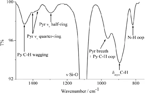
The system was firstly characterized by FT-IR spectra (Figure 2.1.2) using a Jasco FT-IR-430 spectrometer. Four hundred scans (scan range 400–4000 cm-1, resolution 4 cm-1) were collected.
The spectrum shows the N–H out-of-plane peak at 816 cm-1, the C–H bending at 896 cm-1, the pyrrole breathing and the pyridine C–H out-of-plane at 960 cm-1, the pyrrole symmetric half-ring stretching at 1296 cm-1, the pyrrole symmetric quarter-ring stretching at 1376 and 1396 cm-1, and the pyridine CH wagging mode at 1448 cm-1.
16
These peaks are typical of the pyridil porphyrin used for the synthesis of the system and confirm the presence of this molecule on the Si(100)_CA substrate.
Figure 2.1.2. FTIR spectrum of the Si(100)_CA_P in the 750–1550 cm-1 range.
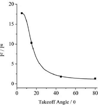
X-Ray photoelectron spectroscopy (XPS) was used to describe the surface elemental composition and the bonding state of the grafted molecules. Angle Resolved X-ray Photoelectron Spectra (AR-XPS) were measured at different (5°, 15°, 30°, 45° and 80°) take-off angles. High resolution spectra were acquired in the range of binding energies (B.E.) related to: C 1s, Si 2p, N 1s, and Cl 2p. Figure 2.1.3 shows the high-resolution N 1s XP spectrum of the Si(100)_CA_P. The fitting of the N 1s signal reveals the presence of two components in a 1 : 7 ratio. These two peaks lie at 399.9 and 402.2 eV. As a consequence, the component at 399.9 eV is assigned as a whole to the four pyrrole nitrogens of the porphyrin core and to three of the four pyridine nitrogens.16 This assignment is in tune with already reported XPS data on porphyrins.17-18 The higher energy component is consistent with a quaternised nitrogen of a pyridine moiety (Scheme 2.1.1).19-23 It emerges that the porphyrin molecule grafts onto the silanized Si(100) substrate using only one pyridine moiety.
17
Figure 2.1.3. Monochromatized Al-K excited AR-XPS of a representative
Si(100)_CA_P in the N 1s binding energy region at a 45° take-off angle.
Using the following equation:
where:
- I represents the XPS peak intensity;
- nN represents the number of N-containing molecules per cm2 in the monolayer;
- is the photoelectron cross-section; - is the inelastic mean free path;
- T(E) is the analyser transmission function of the XPS instrument;
- d is the monolayer thickness (ca. 2.4 nm from morphology characterisation); - is the photoelectron take-off angle
18
Si(100)_CA_P. Taking into account 8 nitrogen atoms per porphyrin molecule, values of 2.4 to 3.6 x 10¹³ (mean value 3.0 x 10¹³) porphyrin molecules per cm2 were obtained. These values are totally consistent with already reported results on similar systems.16
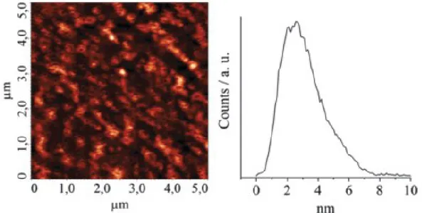
Surface morphology studies were carried out by Atomic Force Microscopy (AFM) and the images were obtained by an instrument manufactured by NT-MTD. The noise level before and after each measurement was 0.01 nm. AFM characterizations were performed in a high-amplitude mode (tapping mode) to avoid any possible modification of the grafted organic layer on the surfaces, caused by the interactions with the tip whose nominal curvature radius is 10 nm. Figure 2.1.4 (left) shows a representative AFM micrograph for a Si(100)_CA_P functionalised substrate.
Figure 2.1.4. AFM image (left) for the representative Si(100)_CA_P monolayer and
related cross-section profile (right).
The micrograph for the Si(100)_CA_P sample shows a relevant number of long structures having a linear arrangement that nucleated and grew-up on the substrate surface. The cross-section analysis (Fig. 2.1.4, right) shows structures whose height (peak-to-peak) is ca. 2.4 nm and widths of 40–60 nm. This structure height is consistent with the size of the CA_P since the silane unit length is 7.2 Å and the porphyrin size obtained by quantum mechanical calculations resulted to be 16.7 Å.24 A few other shorter structures are also apparent because the monolayer set-up is not
19
perfectly homogenous on the molecular scale.25 In fact, the mean height value observed in the AFM cross-section, evaluated across the entire area of Figure 2.1.4, is 1.2 nm (see Density Fuctional Theory, DFT, results). These surface structures evidence a long range order of more than 10 m. Moreover, all the observed structures are parallel to each other thus showing the same direction. This suggests the presence of well-defined porphyrin nanostructures in an upright configuration.
Figure 2.1.5 shows a higher magnification AFM for the representative Si(100)_CA_P monolayer that gives a better idea of the density and size of porphyrin “crystallites” along the linear arrangement.
Figure 2.1.5. High magnification AFM image for the representative Si(100)_CA_P
monolayer showing widths of single domains in the 40–60 nm range.
Finally, to have an idea about the 3D geometrical disposition of the porphyrins in the space after the anchoring to the substrate, accurate DFT quantum mechanical calculations were performed on a single porphyrin–silane system, adopting the closed shell PBE formalism (from Perdew, Burke and Ernzerhof) for both exchange and correlation functionals.26 The standard all-electron 6-31G** basis set was used for all atoms.27 Molecular geometry optimization of stationary points was carried out without symmetry constraints and analytical gradient techniques were used. All calculations
20
were performed using G09 code on linux cluster systems.28 Results indicated that porphyrin molecules are tilted by 67° with respect to the normal to the substrate surface (Figure 2.1.6).
In fact, the pseudo-tetrahedral angle of the benzyl carbon with the quaternized nitrogen is 113° instead of 109°. By taking into account this tilting angle, many structure heights observed with AFM seem to be somewhat larger (ca. 2.4 nm) than those evaluated by DFT (ca. 1.2 nm). But, the mean height value observed in the AFM cross-section, evaluated across the entire area of Figure 2.1.4, is 1.2 nm, consistent with the value estimated on the basis of the DFT results.
Figure 2.1.6.DFT optimization of the Si(100)_CA_P grafting geometry.
We already anticipated that the monolayer set-up is not perfectly homogenous on the molecular scale therefore, it is likely that in this monolayer there are porphyrin molecules either tilted or in the up-right grafting geometry. Both tilted and up-right arrangements should continue to promote good stacking between rings of vicinal porphyrins. The computed footprint of a single porphyrin molecule of 210 Å2 is broadly compatible with its XPS evaluation (330 Å2, obtained from 3.0 x 10¹³ porphyrin molecules per cm2) when, according to the AFM cross-section profile, about 60% surface coverage is taken into account.
21
In order to verify whether porphyirins covalently bound to the substrates hold the luminescence properties, fluorescence measurements were carried out using a Varian Cary Eclipse Fluorescence spectrophotometer with a exc of 420 nm and at 1 nm
resolution, at room temperature. The emission was recorded at 90° with respect to the exciting line beam using 10:10 slit-widths. Spectra were collected at room temperature. Particularly, Figure 2.1.7 shows two strong emissions at = 663 and 718 nm. These results are in agreement with already reported measurements on porphyrin monolayers assembled on solid substratesand confirm that the observed packing due to directional – stacking and other more complex forces does not quench the photoluminescence properties.29-30
Figure 2.1.7. Photoluminescence spectrum of Si(100)_CA_P.
2.1.3 Results and Discussion
From the overall data analysis it results evident that a quite ordered monolayer of porphyrins on silanized Si(100) was grown. Since no discrete bonds are expected between the porphyrin single molecules, probably vicinal porphyrin molecules interact to align the rings and allow – stacking. This interaction leads to an overlap between the electronic states of individual porphyrin units. Moreover, the width of these
22
nanostructures could be due to inter-chain van der Waals and/or additional lateral – stacking interactions between the pyridine moieties. These lines are similar to styrene structures on the order of nm observed on Si(111) engineered substrates and reported in literature.31 In fact, Lopinski et al. reported on the growth of straight molecular styrene lines and proposed that the crystalline silicon substrate determines both the orientation of the lines and the molecular spacing within them.32 The method described for self-directed growth of molecular nanostructures on silicon should allow parallel fabrication of identical complex functional structures and could be sufficiently controllable to be useful in forming and/or connecting nanostructures.32
According to recent published works, ordered structures of polystyrene, in the m range, on Si(111) engineered substrates have been also observed.33-34 Other studies reported on the self-assembly properties of particular porphyrins, thus demonstrating that the strong porphyrin–substrate interaction enables a broader variety of structures35 and that, the occurrence of porphyrins, assembled into patterns, depends on the interplay between directional hydrogen-bonding interactions and packing forces, including molecule–molecule and molecule–substrate interactions.36 Taking into account the crosslinking ability of the trichloro[4-(chloromethyl)phenyl]silane molecules during the surface grafting it seems that the silane functionalised Si(100) template monolayer may encourage this order to the present porphyrin nanostructures.37-38
The most important result obtained from this study is that Si(100)_CA_P shows porphyrin nanostructures with a longer order range, more than 10 m , than that observed in other systems and, despite molecule-molecule interaction, porphyrins preserve single molecule properties, such as their luminescence. Therefore such a system could be useful in the optoelectronic field.
23
2.2 Dynamics of the Chemical Communication
between a Solid Nanoarchitecture and Cu(II)
solutions
Chemical communication may comprise very intricate processes that allow biological organisms and inorganic systems to transfer information.39 An interesting aspect of SRMs is the ability to communicate with the surrounding environment and produce outputs that can be read-out in a fast and precise way. In this context the optical read-out is one of the most reliable procedures. There exist many recent studies of intermolecular communication within thin films.40-42 An example of chemical communication between metal-complex based monolayers is represented by the study of van der Boom.43 Moreover some attention has been paid to the transfer of information between self-assembled organic or polymeric surfaces.44-48 Additional examples refer to the electrochemical reaction along the solid–liquid–gas interface,49 binary logic with synthetic molecular and supramolecular species,50 integration of chemical logic gates,51-53 surface reactions of self-assembled silane monolayers,54 and molecular computing. 54
In this context it was studied the communication between a porphyrin monolayer and different amounts of dilute copper(II) solutions to find out the involved dynamics. This is an example of a stimuli responsive porphyrin monolayer (hardware) subjected to the Cu(II) stimulus (input). The optical readout (output) was indicative of the degree of the communication (reaction) that it was possible to control. It was assembled a covalent monolayer of 5,10,15,20-tetrakis(4-hydroxyphenyl)-21H,23H-porphine (H2THPP) (Figure 2.2.1)on a previously silanized quartz substrate in order to get the H2THPP_SAM system. 39
24
Figure 2.2.8. Structure of the
5,10,15,20-tetrakis(4-hydroxyphenyl)-21H,23H-porphine.
2.2.1 Synthesis of a SAM of Porphyrin
Freshly silanized substrates were immersed in an acetonitrile H2THPP 6.5 x 10⁻⁴ M solution and kept at 70 °C for 70 h while stirring. The H2THPP_SAM formed was left to cool to room temperature and then sonicated 15 min with CH3CN to remove any
residual unreacted porphyrin (Scheme 2.2.1, left).
25
2.2.2 Characterization of a SAM of Porphyrin
The system was widely characterised by AR-XPS (5°, 15°, 45° and 80° take-off angles).
Figure 2.2.2 shows the fitting of the XP spectrum in the O 1s B.E. region of the H2THPP_SAM. Apart the main peak, due to the oxygen of the SiO2 (quartz) substrate,
two other additional peaks at 533.0 and 532.1 eV were essential for the fit. Moreover, the fit revealed identical intensity for these two peaks.
Figure 2.2.2. Monochromatized Al-Kα excited XPS of a representative
H2THPP_SAM in the O 1s binding energy region at 45° take-off angle. The experimental spectral data points (open circles) are fitted with three dominant gaussians at 532.1 eV (cyan line), 533.0 eV (magenta line) and 533.2 eV (blue line). The red line superimposed to the experimental profile refers to the sum of the Gaussian components.
On the basis of previously reported data, these two peaks are consistent with the presence of phenol and ether functions. Therefore it emerges that the tetra-hydroxyphenyl-porphine on the H2THPP_SAM shows two phenol and two ether functions thus suggesting a grafting geometry involving two by four phenol groups (Scheme 2.2.1). This result is totally in agreement with already reported data on similar studies.29
26
Figure 2.2.3 (black line) shows the XP spectrum of the H2THPP_SAM in the N 1s binding energy region and it is evident the broad 1 + 3 band convolution with signals at 398.5 and 400.1 eV, typical of unmetalled porphyrins.55-56
Figure 2.2.3. Al-Kα excited XPS of the as synthesized H2THPP_SAM (black line)
and CuTHPP_SAM (red line) in the N 1s binding energy region at a 45 degree take-off angle.
Figure 2.2.4 shows the AR-XPS angular dependence of the IC/ISi intensity ratios
(IC and ISi are the total intensities of carbon and silicon, respectively) vs. the
photoelectron take-off angle for the H2THPP_SAM.48, 55-60 The ratios exponentially decrease with the take-off angle, , consistently with the presence of a carbon overlayer on SiO2. The IC/ISi intensity ratio can be modelled as follows:
sen d Si sen d C Si C C p Si C s C
e
I
e
I
I
I
2 1)
1
(
27
carbon overlayer and the IC/ISi is the ratio of the Wagner sensitivity factors. The
obtained d value is 27.4 ± 1.5 Å and is highly consistent with the presence of a monolayer of porphyrin molecules perpendicularly grafted on SiO2.
Figure 2.2.4. AR-XPS IC/ISi ratios vs the photoelectron take-off angle of the
H2THPP_SAM. The R2 value of the fit is 0.998.
The value of the thickness is also confirmed by the AFM measurements. In fact from morphology measurements of a representative H2THPP_SAM it emerges that the surface is rather homogeneous with a 2.61 ± 0.15 nm average height and a rootmean-square roughness of 0.72 nm (Figure. 2.2.5).
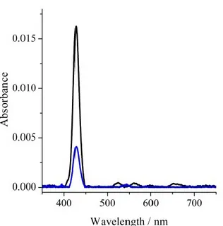
The H2THPP_SAM surface coverage was obtained by UV-Vis measurements. Acetonitrile H2THPP solutions in the 10-7-10-9 M range, with absorbances in the order of 10-2, (similar to those observed for the present H2THPP_SAM) were used for a correct evaluation of the molar extinction coefficient, (Figure 2.2.6, black line). The same procedure was carried out for diluted (10-7-10-9M) acetonitrile CuTHPP solutions (Figure 2.2.6, red line). All UV-Vis measurements were carried out with a 0.2 nm resolution at 25 °C using a diode-array Agilent 8453 spectrophotometerand the optical spectra were simulated using the ReactLab and Hyperquad software packages.57-60
28
Figure 2.2.5. AFM image of the representative H2THPP_SAM (left) and related
cross-sectional profile (right).
Figure 2.2.6. UV-Vis absorption spectra of acetonitrile H2THPP 1.37 x 10⁻⁷M (black line) and CuTHPP 1.19 x 10⁻⁷M (red line) solutions.
The obtained value for PPis 572200 M-1cm-1 (at 418 nm) and 155500 M
-1cm-1 (at 416 nm) for CuTHPP. The value found forPP was used for
calculating the porphyrin density by means of the Beer–Lambert law A =ε lc, where A is the absorbance and ε, l and c are the extinction coefficient, the thickness of the film
29
and the concentration of the molecules in the film, respectively. The obtained surface coverage, dsurf = A -1 (number of molecules per cm2), in H2THPP_SAM is 8.6 x 10¹²
molecules/cm2.61 This means 2.75 x 10¹³ molecules or 4.57 x 10⁻¹¹ mol per substrate. This value is highly consistent with others reported on similar porphyrin monolayer systems.62 In fact the resulting footprint of each porphyrin molecule (1160 Å2) is three times larger than that estimated using the ChemBio3D program (360 Å2) for a compact surface arrangement and this indicates the absence of significant aggregation phenomena and that the monolayer can be enough permeable.
2.2.3 Chemical Communication between a SAM of
Porphyrin and Cu(II) solutions
The ability of H2THPP_SAM to chemically communicate with the surrounding environment was investigated by a complexation reaction between the present H2THPP_SAM and Cu(II) (Scheme 2.2.1), using aliquots of two acetonitrile Cu(AcO)2 solutions having concentrations of the order of 10-6 and 10-4 M. Acetonitrile
is a solvent that shows high affinity for both porphyrin and Cu(II) acetate. This experiment allowed to go deep inside the chemical reactivity of a system that differs from both classical homogenous and not-homogeneous reactants. In fact, it is known that a molecular monolayer cannot be envisaged as a solid bulk system, since single molecules possess a good degree of freedom, nor as a gaseous system since the grafted molecules are bound to the substrate surface. As a consequence the involved chemical reactivity can be rather different with respect to that of the typical chemical reaction media.
During the UV-Vis measurements the substrate (2 x 0.8 cm) bearing on both sides the porphyrin monolayer (whole area = 3.2 cm2) was set inside a quartz cuvette using an appropriate Teflon substrate holder, (Figure 2.2.6), and 2.5 mL of acetonitrile were added to cover the substrate. The reference cuvette contained a silane functionalised quartz substrate on another Teflon substrate holder and 2.5 mL of acetonitrile. Then, increasing amounts of copper(II) acetate acetonitrile solutions (Table 2.2.1) were
30
added in both cuvettes using a precision burette (Hamilton, 1000 mL). After each addition, the system was allowed to equilibrate for 4 min prior to UV-Vis measurements. In particular, two 2.5 x 10⁻⁶ and 2.5 x 10⁻⁴ M copper acetonitrile solutions were used and 28 spectra were recorded for this experiment. The data, corrected for the volume variation, were subsequently analysed by using two different software packages namely ReactLab35 and Hyperquad36 that make use of a multiwavelength and multivariate treatment of spectral data.57-60
Figure 2.2.6. Set-up for UV-Vis measurements of the quartz substrate bearing a
porphyrin monolayer.
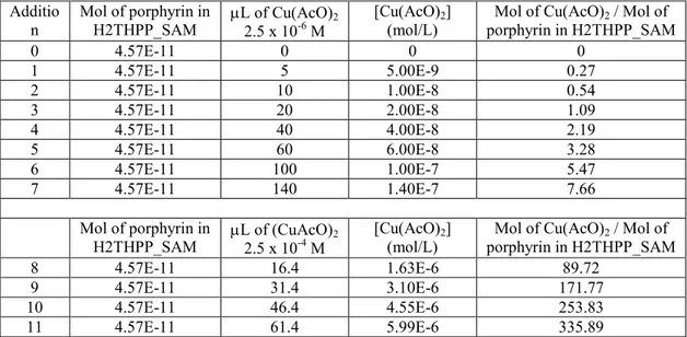
Table 2.2.1. Additions of copper(II) acetate acetonitrile solutions for the conversion of
the H2THPP_SAM in CuTHPP_SAM.
Additio
n Mol of porphyrin in H2THPP_SAM L of Cu(AcO)2.5 x 10⁻⁶ M 2 [Cu(AcO)(mol/L) 2] porphyrin in H2THPP_SAM Mol of Cu(AcO)2 / Mol of
0 4.57E-11 0 0 0 1 4.57E-11 5 5.00E-9 0.27 2 4.57E-11 10 1.00E-8 0.54 3 4.57E-11 20 2.00E-8 1.09 4 4.57E-11 40 4.00E-8 2.19 5 4.57E-11 60 6.00E-8 3.28 6 4.57E-11 100 1.00E-7 5.47 7 4.57E-11 140 1.40E-7 7.66 Mol of porphyrin in
H2THPP_SAM L of (CuAcO)2.5 x 10⁻⁴ M 2 [Cu(AcO)(mol/L) 2] porphyrin in H2THPP_SAM Mol of Cu(AcO)2 / Mol of
8 4.57E-11 16.4 1.63E-6 89.72 9 4.57E-11 31.4 3.10E-6 171.77 10 4.57E-11 46.4 4.55E-6 253.83 11 4.57E-11 61.4 5.99E-6 335.89
31 12 4.57E-11 76.4 7.41E-6 417.94 13 4.57E-11 91.4 8.82E-6 500.00 14 4.57E-11 106.4 1.05E-5 582.05 15 4.57E-11 121.4 1.16E-5 664.11 16 4.57E-11 136.4 1.29E-5 746.17 17 4.57E-11 151.4 1.43E-5 828.23 18 4.57E-11 166.4 1.56E-5 910.28 19 4.57E-11 181.4 1.69E-5 992.34 20 4.57E-11 196.4 1.82E-5 1074.40 21 4.57E-11 211.4 1.95E-5 1156.45 22 4.57E-11 226.4 2.07E-5 1238.51 23 4.57E-11 241.4 2.20E-5 1320.57 24 4.57E-11 256.4 2.32E-5 1402.62 25 4.57E-11 271.4 2.45E-5 1484.68 26 4.57E-11 286.4 2.57E-5 1566.74 27 4.57E-11 301.4 2.69E-5 1648.80 28 4.57E-11 316.4 2.81E-5 1730.85
Finally, the system was characterized by XPS measurements. In particular, Figure. 2.2.2 (red line) shows a narrow and symmetric N 1s signal at 400.3 eV that is due to the equivalence of the porphyrin nitrogens upon the CuTHPP_SAM formation in which the copper complex has a local D4h symmetry. The XPS atomic concentration
analysis of the CuTHPP_SAM shows a N/Cu atomic ratio of 4.5 consistent with the 9% of the starting H2THPP_SAM and the 91% of the CuTHPP_SAM.
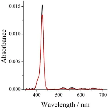
Figure. 2.2.7 describes the optical behaviour of the H2THPP_SAM upon three selected Cu(AcO)2 additions. The starting Soret band at 427.6 nm shows a 9.6 nm red
shift upon the porphyrin grafting with respect to the solution measurement. Moreover, the most dilute solution allowed to investigate the reaction pathway up to 50.0% of the total Abs variation (Abs = 0.012) observed in experiments. In fact, after the addition of 3.5 x 10⁻¹⁰ mol of Cu(AcO)2 (Table 1.1, [Cu(II)] = 1.40 x 10⁻⁷) it was noted that the
absorbance decreased to 0.01 (Abs50) (Figure 2.2.7, red line) and this corresponds to
the 61% of its initial intensity value (Abs100 = 0.016) (Figure 2.2.7, black line) and to
the 50.0% of the total Abs variation. After the addition of 7.9 x 10⁻⁸ mol of Cu(AcO)2
(Table 2.2.1, [Cu(II)] = 2.81 x 10⁻⁵) the Abs value was 0.004 (Abs0) (Figure 2.2.7, blue
line) and this corresponds to the 25.0% of its initial intensity value. No other Abs variation was observed upon further Cu(AcO)2 addition.
32
related to three absorbance values (0.016, 0.010 and 0.004) that can be used as thresholds and correspond to three different (mol of porphyrin in H2THPP_SAM) / (mol of the porphyrin Cu(II) complex in CuTHPP_SAM) ratios. Thus the present H2THPP_SAM may find potential interest for permanent memory storage. In fact, the observation of three distinct optical states Abs100, Abs50, and Abs0, as a function of the
[Cu(AcO)2] concentration, can be exploited for integration of this ternary memory
state system in optical devices.
Figure 2.2.7. UV-Vis spectra H2THPP_SAM upon three selected Cu(AcO)2 additions.
Figure 2.2.8 shows the overall optical variation of the H2THPP_SAM upon the Cu(AcO)2 additions (Table 2.2.1). Therefore, the Soret (B-band) suffers a monotonic
hypochromic effect consistent with the formation of the CuTHPP_SAM. The spectral changes, evident upon the Cu(AcO)2 additions, can be interpreted in terms of the
convolution of two Soret bands belonging to the H2THPP_SAM and CuTHPP_SAM whose values are significantly different (572200 and 155500 M-1 cm-1, respectively).
The optical spectra in the Q-band region of the H2THPP_SAM upon the Cu(AcO)2 additions show a decreased number of Q-bands (Figure 2.2.9, blue line).
33
the 545.4 and 587.4 nm new bands. This observation is in agreement with the formation of the CuTHPP (Scheme 2.2.1, right).
Figure 2.2.8. UV-Vis spectra of the H2THPP_SAM during the Cu(AcO)2 additions.
Figure 2.2.9. UV-Vis spectra of the starting H2THPP_SAM (black line) and upon
2.81 x 10⁻⁵ mol/L of Cu(AcO)2 addition (blue line).
34
additions. In particular, Figure 2.2.10a shows the relative variations upon the addition of the most dilute 2.5 x 10⁻⁶ M Cu(AcO)2 solution and Figure 2.2.10b shows the
relative variations upon the addition of the 2.5 x 10⁻⁴ M Cu(AcO)2 solution. In both
cases almost linear behaviours are evident. These optical trends are highly desired. In fact, to exploit the ability of the present H2THPP_SAM nanoarchitecture to communicate with the solution, linear behaviour (outputs) upon external stimuli (inputs) easily allows the signal transduction to process the information and thus the development of devices useful in many important technological fields.
Figure 2.2.10. Relative absorbance variations during the 2.5 x 10⁻⁶ M (a) and 2.5 x 10
-4 M (b) Cu(AcO)
2 additions. The R2 values of the fits are (a) 0.96 and (b) 0.97.
It was also determined the stability constant of CuTHPP_SAM using the spectrophotometric experiment related to the following dynamic equilibrium reaction:
H2THPP_SAM + Cu(AcO)2 ↔ CuTHPP_SAM + 2AcOH log K = 5.80
and it was found that the system shows a fairly high stability constant value (631000). This indicates the involvement of the four nitrogen atoms of the porphyrin ring in the
35
copper(II) coordination sphere. Interestingly, this value is in good agreement with already reported stability constants for similar solution reactions.63
Figure 2.2.11 shows the distribution diagram of the H2THPP_SAM and CuTHPP_SAM species obtained with the HYSS software package by simulating different additions of a unique 2.5 x 10⁻⁴M Cu(AcO)2 solution.64 It can be noticed that
the system forms only one complex species and the [H2THPP_SAM] / [CuTHPP_SAM] ratio = 1 at = 0.5 can be obtained when the concentration of the [Cu(AcO)2] is 1.63 x 10⁻⁶. Indeed, this corresponds to the experimental cumulative
Cu(AcO)2 concentration reached after the first addition of the more concentrated
solution in the reaction media (16.4 L of Cu(AcO)2 2.5 x 10⁻⁴ M, Table 2.2.1). After
271.4 L of Cu(AcO)2, when the [Cu(AcO)2] is 2.45 x 10⁻⁵, only the 6% of the starting
H2THPP_SAM remained and the CuTHPP_SAM is now the 94% of the starting concentration.
Figure 2.2.11. Distribution diagram of the [H2THPP_SAM] and [CuTHPP_SAM]
calculated with the HYSS software package. Abscissa (bottom) shows both the [Cu(AcO)2] concentration and the corresponding volume addition of the 2.5 x 10⁻⁴ M
Cu(AcO)2 solution. The top abscissa shows the experimental absorbance
36
These calculated values are in close agreement with the experimental XPS evaluation based on the atomic concentration analysis. It emerges that each optical absorbance corresponds to a particular [H2THPP_SAM] / [CuTHPP_SAM] ratio.
In addition, the speciation study for this porphyrin and copper(II) was also carried out for acetonitrile H2THPP solutions (Figure 2.2.12).
Figure 2.2.12. UV-Vis measurements of the acetonitrile H2THPP 1.37 x 10⁻⁷ M solution (2 mL) during the additions (5-200 L) of the 3.62 x 10⁻⁴ M acetonitrile solution of Cu(AcO)2.
In particular, Figure 2.2.13 shows three UV-Vis spectra registered during the solution H2THPP titration experiment: the starting spectrum (black line), the intermediate (blue line) and the final (red line). It is possible to note Abs variations in the Soret and in the Q-bands region. In detail, the initial 4 Q-bands at 515.6, 556.2, 594.0 and 648.6 nm respectively, reduce to two new bands at 544.2 and 581.6 nm upon Cu(II) additions, as similarly observed for the H2THPP_SAM.
From the Abs data obtained during the solution titration it was calculated the log K value for such reaction and it was obtained a log K of 5.21 (stability constant = 162181), significantly smaller than that obtained for the H2THPP_SAM (log K = 5.80). This result suggests that the grafted complex is more stable than that formed in
37
solution probably owing to the lower ability of the cofacial molecules in CuTHPP_SAM to dissociate, and also because the preformed cofacial arrangement of the molecules facilitates the binding of the metal ion.63
Figure 2.2.13. UV-Vis measurements of the acetonitrile H2THPP 1.37 x 10⁻⁷ M (2 mL) before (black line) and after the additions of 24 (blue line) and 200 (red line) L of the 3.62 x 10⁻⁴ M acetonitrile solution of Cu(AcO)2.
In summary H2THPP_SAM is a robust and stable SRM system that produces readable optical output upon external chemical stimuli. Each optical output corresponds to a precise chemical composition, namely a precise stable physical state. Therefore, such nanostructured system could have potential application for multi-bit information storage devices.
38
2.3 Porphyrins Functionalised TiO2 and SnO2
Nanocrystals
Nowadays the production of energy that satisfies the worldwide requirement is a need of the modern society. Renewable sources, as biofuels, biomasses, isothermal, geothermal, hydropower and solar energies are eco-friendly thus preferable. The solar energy impinging on the earth corresponds to 2.9 × 10¹² TJ/year and that value overwhelms about 6.000 times the actual world annual need. Therefore it is not surprising that during the last decade attention was focused on the solar energy as major source for the energy production for the worldwide consumption.
In this context, photovoltaic devices, such as the dye sensitised solar cells, convert visible light to electrical energy.65-72 In this technology the most used anode inorganic substrates are the transparent conducting oxides (TCOs) such as SnO2 and TiO2. 74-75
SnO2 is a prototype oxide that adopts the tetragonal rutile structure (lattice parameters
a= 4.737Å, c= 3.369 Å), belongs to the D144h space group and contains two formula
units per cell. In the SnO2 there is a good level of metal-oxygen covalency that
involves the diffuse Sn 5s and 5p atomic orbitals.73 This covalency, in turn, causes a band-gap of 3.6 eV and a large O 2p valence band width (10 eV).73 In TiO2 the
band-gap is 3.1 eV and the O 2p valence band width is 6.3 eV.73 These differences are due to the fact that the conduction band states in TiO2 are Ti 3d in nature whilst in SnO2
involve the more diffuse Sn 5s and 5p levels. The attractive properties displayed by these nanostructures are based on their atomic scale structures and can be tailored for appropriate physico-chemical properties.76 For example, low dimensional SnO2
nanowires and nanobelts are highly sensitive and efficient transducers of surface chemical processes into electrical signals.77-78 As anticipated above, porphyrins assembled on TiO2 or SnO2 play a leading role in the DSSC technology. If these dyes
are physisorbed on the oxide surfaces, through-space electron interactions dominate.79 In contrast, if the dyes are covalently assembled on the oxide surfaces,80-82 through-bond electron interactions dominate thus increasing the device efficiency.79 In fact,
39
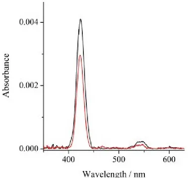
these covalent systems overcome the problem of loss of efficiency during the electron injection since the dye layer is directly in contact (covalent) with the semiconductor surface.65 Therefore well-organized porphyrin molecules, covalently anchored to appropriate nanosized conducting inorganic oxides, are promising materials for the next generation of molecular-based DSSC devices. In this perspective, the synthesis, characterization and optical properties of the free-base porphyrin H2THPP or its copper complex CuTHPP covalently assembled on TiO2 and SnO2 (hereafter,
H2THPP_TiO2, H2THPP_SnO2, CuTHPP_TiO2 and CuTHPP_SnO2, respectively)
were studied. To investigate the donor–acceptor effect between the porphyrin monolayers and the metal oxide the luminescence spectra of the different functional nanostructures presently synthesized were compared and it is announced that covalency between dye and semiconducting nanocrystals plays a fundamental role in the electron injection and in all cases the SnO2 functionalised nanocrystals disclose the
best donor–acceptor behaviour.1
2.3.1 Synthesis of Porphyrin Nanostructures on TiO
2and
SnO
2The synthetic strategy already used for the covalent functionalization of flat substrates was adopted also in this case (Scheme 2.3.1). In detail, TiO2 and SnO2 white
powders (Aldrich) were annealed overnight to 600°C in a furnace using recrystallised alumina crucibles and then, left to cool to room temperature and transferred in a glove-box under a N2 atmosphere (1ppm H2O, 1 ppm O2). At that point, the single TiO2 and
SnO2 powders were dispersed at room temperature in two n-pentane solutions (100 mL
per each) 0.2 : 100 v/v of the silane coupling agent, soon removed from the glove-box in sealed flasks and sonicated for 60 min (25°C) to afford a CA monolayer on each crystal grain.56 Afterward, the powder-containing flasks were moved back into the glove-box and the powders were decanted and washed with n-pentane 10 times while stirring. Then, they were removed from the glovebox and heated up to 135 °C for 15 min in an oven to complete the CA grafting. Subsequently, the powders were sonicated
40
twice in pentane for 5 min (25°C) to remove any eventual remaining physisorbed CA, decanted and transferred again in the glovebox. Then they were immersed into stirred 3.5 10-4 M CH3CN 100 mL solutions of H2THPP, removed from the glovebox in
sealed flasks, and sonicated for 7 h while heating at 50 °C. Then, the flasks were removed from the sonicator and heated-up to 70°C while stirring on an IKA RCT hotplate for 120 h. Similarly, some silanized TiO2 and SnO2 powders were left also to
react with a 4.6 x 10⁻⁴ M CH3CN solution of CuTHPP.
Scheme 2.3.1. Reaction pathway for TiO2 and SnO2 nanoparticles functionalised with
a monolayer of H2THPP or CuTHPP.
Lastly, each suspension of the porphyrin (or CuTHPP) functionalised TiO2 and
SnO2 was cooled to room temperature and subjected to multiple cycles of
sonication/centrifugation-filtration until there was no UV-Vis evidence of any residual porphyrin in the remaining solutions. Each sonication (10 min) was performed in CH3CN and the related centrifugation-filtration was achieved using a column
41
molecular weight cut-off, to remove any residual unreacted porphyrin. The filtration column was positioned at a fixed 25° angle in the centrifuge and, when subjected to 5000 rpm, the internal membrane restrains particles having a MWCO 3000. Pale yellow-green or pink nanocrystals were obtained for H2THPP or CuTHPP functionalised oxides, respectively.
The adopted synthetic procedure involves the sonication of the solutions during the powder silanization process since this reduces the presence of grain agglomerates. In addition, the sonication during the first 7 hours of reaction of the silanized grains with the porphyrin solutions is helpful in avoiding the formation of silanized oxide grain aggregates. Moreover, the sonication should partially prevent also some porphyrin aggregation due to the well-known stacking effect. Finally, the reaction time for the porphyrin grafting was much larger (120 h) than that typically used (Scheme 2.3.1).56
2.3.2 Characterization of Porphyrin Nanostructures on
TiO
2and SnO
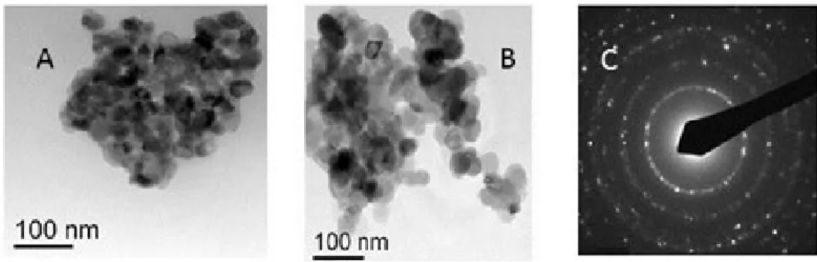
2The functionalised oxides were characterised by XPS, IR, UV-Vis, luminescence and Transmission Electron Microscopy (TEM) measurements.
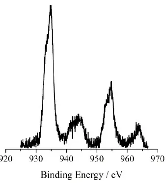
Figure 2.3.1 shows the XP spectrum of the TiO2 after the H2THPP grafting in the
Ti 2p binding energy region. The two well resolved peaks at 459.3 and 465.1 eV represent the spin-orbit components of the Ti 2p3/2,1/2 states, respectively. These values
are about 0.8 eV at higher B.E. with respect to those measured for pure TiO2 annealed
overnight at 600°C under a continuous 100 sccm (standard cubic centimetres per minute) flux of oxygen and that are typical of pure titania: Ti 2p3/2 = 458.5, 2p1/2 =
464.3 eV.
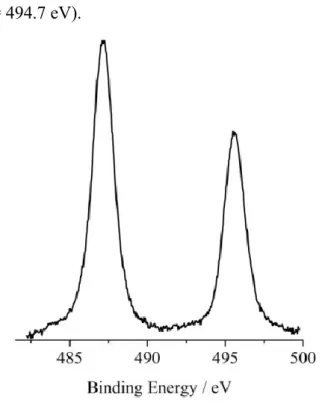
Figure 2.3.2 shows the XP spectrum of the SnO2 after the H2THPP grafting in the
Sn 3d binding energy region. The two well resolved peaks at 487.1 and 495.5 eV represent the spin-orbit components of the Sn 3d5/2,3/2 states.56 Also in this case the
observed values are at 0.8 eV higher B.E. with respect to those we measured for pure SnO2 annealed overnight at 600°C under a continuous 100 sccm flux of oxygen (Sn
42 3d5/2 = 486.3, 3d3/2 = 494.7 eV).
Figure 2.3.1. Al-Kα excited XPS of the H2THPP_TiO2 in the Ti 2p binding energy
region.
Figure 2.3.2. Al-Kα excited XPS of the H2THPP_SnO2 in the Sn 3d binding energy
region.
In contrast to these observations, the XPS N 1s main peak of both the H2THPP_TiO2 and H2THPP_SnO2 (Figure 2.3.3) lies at 400.1-400.2 eV that is at