Scuola di Dottorato in Ingegneria “Leonardo da Vinci”
Corso di Dottorato di Ricerca in
Ingegneria dell'Informazione
Tesi di Dottorato di Ricerca
Embedded computing systems design:
architectural and application
perspectives
Tony Salvatore Bacchillone
Scuola di Dottorato in Ingegneria “Leonardo da Vinci”
Corso di Dottorato di Ricerca in
Ingegneria dell'Informazione
Tesi di Dottorato di Ricerca
Embedded computing systems design:
architectural and application
perspectives
Autore:
Tony Salvatore Bacchillone ____________________
Relatori:
Prof. Luca Fanucci ____________________
Prof. Sergio Saponara ____________________
S
OMMARIOQuesto elaborato affronta varie problematiche legate alla progettazione e all'implementazione dei moderni sistemi embedded di computing, ponendo in rilevo, e talvolta in contrapposizione, le sfide che emergono all'avanzare della tecnologia ed i requisiti che invece emergono a livello applicativo, derivanti dalle necessità degli utenti finali e dai trend di mercato.
La discussione sarà articolata tenendo conto di due punti di vista: la progettazione hardware e la loro applicazione a livello di sistema.
A livello hardware saranno affrontati nel dettaglio i problemi di interconnettività on-chip. Aspetto che riguarda la parallelizzazione del calcolo, ma anche l'integrazione di funzionalità eterogenee. Sarà quindi discussa un'architettura d'interconnessione denominata Network-on-Chip (NoC). La soluzione proposta è in grado di supportare funzionalità avanzate di networking direttamente in hardware, consentendo tuttavia di raggiungere sempre un compromesso ottimale tra prestazioni in termini di traffico e requisiti di implementazioni a seconda dell'applicazione specifica. Nella discussione di questa tematica, verrà posto l'accento sul problema della configurabilità dei blocchi che compongono una NoC. Quello della configurabilità, è un problema sempre più sentito nella progettazione dei sistemi complessi, nei quali si cerca di sviluppare delle funzionalità, anche molto evolute, ma che siano semplicemente riutilizzabili. A tale scopo sarà introdotta una nuova metodologia, denominata Metacoding che consiste nell'astrarre i problemi di configurabilità attraverso linguaggi di programmazione di alto livello. Sulla base del metacoding verrà anche proposto un flusso di design automatico in grado di semplificare la progettazione e la configurazione di una NoC da parte del designer di rete.
Come anticipato, la discussione si sposterà poi a livello di sistema, per affrontare la progettazione di tali sistemi dal punto di vista applicativo, focalizzando l'attenzione in particolare sulle applicazioni di monitoraggio remoto. A tal riguardo saranno studiati nel dettaglio tutti gli aspetti che riguardano la progettazione di un sistema per il monitoraggio di pazienti affetti da scompenso cardiaco cronico. Si partirà dalla definizione dei requisiti, che, come spesso accade a questo livello, derivano principalmente dai bisogni dell'utente finale, nel nostro caso medici e pazienti. Verranno discusse le problematiche di acquisizione, elaborazione e gestione delle misure. Il sistema proposto introduce vari aspetti innovativi tra i quali il concetto di protocollo operativo e l'elevata interoperabilità offerta. In ultima analisi, verranno riportati i risultati relativi alla sperimentazione del sistema implementato.
Infine, il tema del monitoraggio remoto sarà concluso con lo studio delle reti di distribuzione elettrica intelligenti: le Smart Grid, cercando di fare uno studio dello stato dell'arte del settore, proponendo un'architettura di Home Area Network (HAN) e suggerendone una possibile implementazione attraverso Commercial Off the Shelf (COTS).
A
BSTRACTThis work deals with embedded computing design, highlighting both: typical challenges coming from technology advances and system requirements concerning the application level. The second ones generally result from end-user needs and market trends.
The discussion takes into account two main points of view: the hardware design and the application or system level design.
Concerning the hardware point of view, the on-chip interconnection will be studied in the detail. This aspect is related to computing parallelization and the integration of heterogeneous functionalities. An interconnection architecture known as Network-on-Chip (NoC) will be discussed. An innovative NoC, offering advanced networking functionalities directly implemented in hardware, will be introduced. The proposed design offers a high flexibility allowing always finding the optimal trade-off between network performances and implementation requirements (derived from specific application). This part will mainly focus on the configurability of the NoC building blocks. Design configurability and reusability is becoming more and more important with the increasing design complexity. In order to effectively address this issue, an innovative methodology called Metacoding will be introduced. This methodology consists on the abstraction of the configuration intents using a high-level programming language. Moreover, an automatic design flow based on the metacoding methodology will be proposed. The developed framework simplifies the design and the configuration of a NoC for a network designer.
Concerning the system level point of view, remote monitoring applications will be discussed. This part will focus in particular on the design of a telemonitoring system for patients affected by chronic heart failure. Particular attention will be paid to the system requirements definition coming from end-users: in our case, clinicians and patients. The proposed system is based on an innovative Operating Protocol. The use of well-known communication protocols and standards favours the maximum interoperability with others systems. Vital signals acquisition, data processing and collection will be discussed. Finally, the results of the demonstration phase, involving real patients and clinicians, will be reported. An exploration of energy monitoring for Smart Grids closes the discussion on remote monitoring applications. After a review of the state of the art, a Home Area Network (HAN) architecture will be proposed, taking into account requirements and security issues; a possible implementation based on Commercial Off the Shelf (COTS) is discussed.
C
ONTENTSSOMMARIO ... VII
ABSTRACT ... IX
CONTENTS ... XI
1
INTRODUCTION: COMPUTING CONCEPTS, TREND AND
CHALLENGES ... 1
1.1
More Moore and More than Moore ... 1
1.2
Design challenges ... 2
1.3
Next generation computing ... 4
1.4
Application Domains ... 6
1.4.1
Healthcare ... 7
1.5
Organization of this work ... 8
2
INTERCONNECTION
ARCHITECTURES
FOR
HETEROGENEOUS MPSOC: NETWORK ON-CHIP ... 11
2.1
Router Features and Architecture ... 13
2.1.1
Topology and Routing ... 13
2.1.2
Architecture ... 14
2.1.3
Buffering and Latency ... 15
2.1.4
Quality of Service ... 16
2.2
Core Network Interface Design ... 16
2.2.1
NI Top-level Architecture ... 17
2.2.2
Kernel-Shell Interface by Bi-synchronous FIFOs ... 19
2.2.3
NI Physical Link and NoC Interface ... 21
2.3
Advanced Network Interface Features ... 23
2.3.1
Store & Forward (S&F) ... 23
2.3.2
Error Management Unit (EMU) ... 24
2.3.3
Power Manager (PM) ... 25
2.3.4
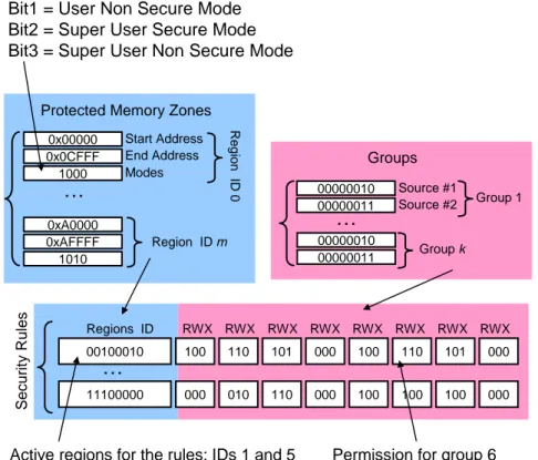
Security ... 26
2.3.5
Ordering Handler ... 28
2.3.6
Remap ... 29
2.3.7
QoS Scheme ... 29
2.3.8
Programming Interface ... 31
2.4
Metacoding design methodology and automatic design
flow ... 33
2.4.1
Router Configuration Space ... 33
2.4.2
NI Configuration Space ... 35
2.4.3
The Metacoding Approach ... 36
2.4.4
Automated Design Flow ... 39
2.5
CMOS Implementation Results ... 40
2.5.1
CMOS Synthesis Results ... 41
2.5.2
Complexity of the NoC vs. the connected IP in real
MPSoC implementations ... 46
3
EFFICIENT APPLICATION DESIGN EXPLORATION ... 49
3.1
Health monitoring system for CHF patients ... 49
3.1.1
H@H Telecare System Overview ... 51
3.1.2
H@H Sensor Devices ... 53
3.1.2.1 ECG-SpO2 module ... 55
3.1.2.2 UA-767BT blood pressure monitor ... 57
3.1.2.3 UA-321PBT digital scale ... 57
3.1.3
IC Front-End for Cardiac Sensors ... 58
3.1.4
H@H Sensor Signal Processing ... 62
3.1.4.1 ECG ... 63
3.1.4.1.1 Basic Feature Extraction ... 64
3.1.4.1.2 Abnormal Heart Frequency ... 65
3.1.4.1.3 Atrial Fibrillation ... 66
3.1.4.2 SpO2 and Plethysmographic wave ... 69
3.1.4.3 Blood pressure ... 70
3.1.4.4 Weight ... 70
3.1.5
Testing and Results ... 71
3.1.6
Comparison with the State of the Art ... 73
3.2
Energy monitoring for Smart grid ... 75
3.2.1
Limits of existing power grid and challenges of Smart
Grid
75
3.2.2
Network architecture ... 78
3.2.3
Security and privacy problems ... 79
3.2.3.1 Practice to secure the HAN ... 82
3.2.3.2 Security standards and proposed solutions ... 83
3.2.4
Home Energy Network Possible Implementation ... 85
3.2.4.1 HW Architectures of Building Nodes: Smart Plugs, Home Energy Angel Box and Smart Power Meters... 89
3.2.4.2 COTS Components Selection to Build the Energy HAN
3.2.4.3 Security in the Proposed ZigBee/802.15.4 HAN ... 96
4
CONCLUSION ... 103
4.1
NoC interconnection architectures for MPSoC ... 103
4.2
Health monitoring system for CHF patients ... 104
4.3
Energy Home Area Network for Smart Grid ... 105
BIBLIOGRAPHY ... 107
LIST OF FIGURES ... 119
LIST OF TABLES ... 123
LIST OF ACRONYMS ... 125
LIST OF PUBLICATIONS ... 129
International peer-reviewed journals ... 129
Conference proceedings ... 129
Filed Patents ... 130
1
INTRODUCTION: COMPUTING CONCEPTS, TREND AND
CHALLENGES
"The number of transistors that can be fabricated on a very large-scale integrated (VLSI) chip doubles approximately every two years". Since its introduction in 1965 by the co-founder of Intel, Gordon Moore, and despite having been fixed during years to match market trends, Moore's Law still keeps its meaning and validity.
In practical terms, the result is that computing performance doubles every 18 months, and has done so for decades, since early 70's, up to the present. The ability of the silicon industry to fulfil Moore's law was mainly achieved by the continuous downscaling of the critical dimensions in the integrated circuit: improvements in semiconductor manufacturing processes allow the fabrication of smaller transistors on wider wafers, thus boosting economies of scale. Above all that, advances in design technologies, design paradigms and design methodologies enable engineers to effectively handle more and more complex designs, bridging the design complexity versus the designer productivity gap.
This chapter lays the groundwork for the topics discussed in this dissertation, by presenting current state of the art and future trends of computing architectures and application domains. An overview of the organization of the whole work closes the chapter.
1.1 More Moore and More than Moore
As introduced in the previous section, from a technology perspective, the continuous increase in the integration density proposed by Moore’s Law was made possible by a dimensional scaling. The transistors scaling brings two main advantages: on the one hand it allows to increase the density of silicon integration and on the other hand it allows to save power thanks to lower capacitance and supply voltage. High density and low power are very important achievements for computing, in particular in case of battery-powered portable electronic devices, which are among the most requested consumer electronic products.
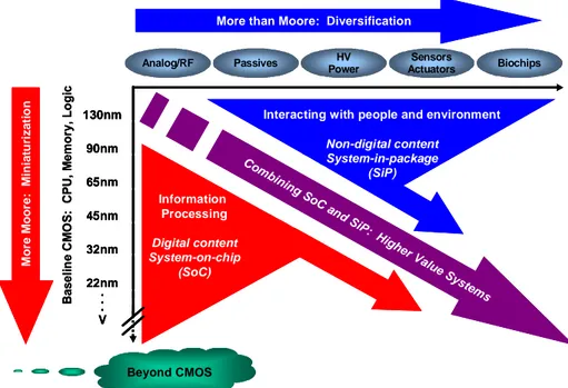
According to the International Technology Roadmap for Semiconductors (ITRS) classification, this trend in circuit miniaturization by scaling down the transistor and its associated benefits in terms of performances is known as “More Moore” [1].
Continued shrinking of physical feature sizes achieved in the More Moore domain, directly impacts on digital functionalities (i.e. microprocessors, memories, and digital logic). This aspect involves around 70% of the total semiconductor component market.
However, a microelectronic device is usually composed of many digital functionalities and non-digital functionalities. In the past, Application Specific Integrated Circuits (ASICs) implemented digital functionalities of a system, while the non-digital functionalities were developed at Printed Circuit Board (PCB) level, with glue logic or analog circuits providing connectivity with the custom chip.
With technology scaling and present progress in both process technology and design, digital functionalities and non-digital functionalities are being crammed in the same package containing the integrated circuit, or even in the chip area.
The combination of multiple functionalities into a single package is generally known as System in Package (SiP). A SiP may contain for example passives, Micro Electro-Mechanical Systems (MEMS), optical components and other packages and devices. On the other side, the integration of digital and non-digital functionalities on a single chip is generally referred to as System On Chip (SoC). A SoC may contain for example digital, analog, mixed-signal, Radio-Frequency (RF) functions, etc.
Non-digital functionalities do not necessarily scale at the same rate as digital ones because of technology scaling. As a consequence, their incorporation does not contribute to the miniaturization of electronic systems. Nevertheless, they provide an additional value in different ways and allow the migration of non-digital functionalities from the system board-level into the package or onto the chip. The combined need for digital and non-digital functionalities in an integrated system is translated by the ITRS as a dual trend and is labelled as “More-than-Moore” [1] (see Figure 1.1).
1.2 Design challenges
The two trends introduced in the previous section arise a stream of challenges to be overcome when designing an electronic system. As a first stage approximation, we can consider that More Moore trend originates challenges
More than Moore: Diversification
M o re M oo re : M in ia tu ri z a ti o n Co mb ining S oC and SiP: H igher Value S ystems B ase li n e C M O S : C P U , M e m o ry , L o g ic Biochips Sensors Actuators HV Power Analog/RF Passives 130nm 90nm 65nm 45nm 32nm 22nm . . . V Information Processing Digital content System-on-chip (SoC) Beyond CMOS
Interacting with people and environment
Non-digital content System-in-package
(SiP)
More than Moore: Diversification
M o re M oo re : M in ia tu ri z a ti o n M o re M oo re : M in ia tu ri z a ti o n Co mb ining S oC and SiP: H igher Value S ystems B ase li n e C M O S : C P U , M e m o ry , L o g ic Biochips Sensors Actuators HV Power Analog/RF Passives 130nm 90nm 65nm 45nm 32nm 22nm . . . V 130nm 90nm 65nm 45nm 32nm 22nm . . . V Information Processing Digital content System-on-chip (SoC) Beyond CMOS
Interacting with people and environment
Non-digital content System-in-package
(SiP)
in terms of complexity because of the growing operational demand. At the same time, More-than-More trend introduces a new set of problems quite often concerning various fields.
The most relevant challenges are:
Design complexity: as circuit complexity grows, design takes much time and it is more expensive. Masks and manufacturing costs become higher and testing costs grow in a comparable way. This issue is dramatically highlighted when considering market effects: design space exploration, mask manufacturing, testing strategies represent an increasing delay for time-to-market, while higher costs can be recovered only with a significant time-market.
Wiring: as a consequence of transistors scaling and their faster switching activity, wires become the bottleneck for integrated circuits. Wires introduce parasitic capacitances that raise their charging time compromising the overall circuit speed. This effect is particularly highlighted for global wires, like clock wiring nets. The number of required wires generally increases with design complexity and, due to crosstalk effects, this may compromise the integrity of the information carried by wires. Thus, front-end synthesis results are no more reliable since the performance strongly depends on how wires are placed and routed along the circuit. The wiring model provided in front-end design space, is not sufficient to predict circuit performance below 90 nm technologies. This means a continuous feedback between pre-layout and post-layout in the project flow.
Communication: point-to-point links and traditional shared buses show significant limitations as the number of integrated functionalities increases. The more functionalities are in the chip, the more communication wirings are needed thus compromising scalability, performance and design time. Furthermore, cores need efficient communication infrastructure to exploit intensive parallel communication and to access shared resources.
Heterogeneity: integration of digital and non-digital functionalities on chip requires dealing with many sub-designs. As discussed, a complex design could foresee the integration of digital, analog, mixed-signal, sensors, radio-frequency functions, etc. in the same chip. This generally implies different expertises to converge in the design group, increasing design space, costs and development time.
Tools: in the last decades electronic industry productivity has been remarkably pushed forward thanks to CAD (Computer Aided Design) tools. Future SoC development poses significant challenges even for CAD tools, since they must support a larger design space and an increased complexity over functionality. Moreover, an important challenge is also related to verification activities, where simpler techniques are required together with faster and more accurate simulation engines. As the design paradigms evolve even new services of CAD are needed.
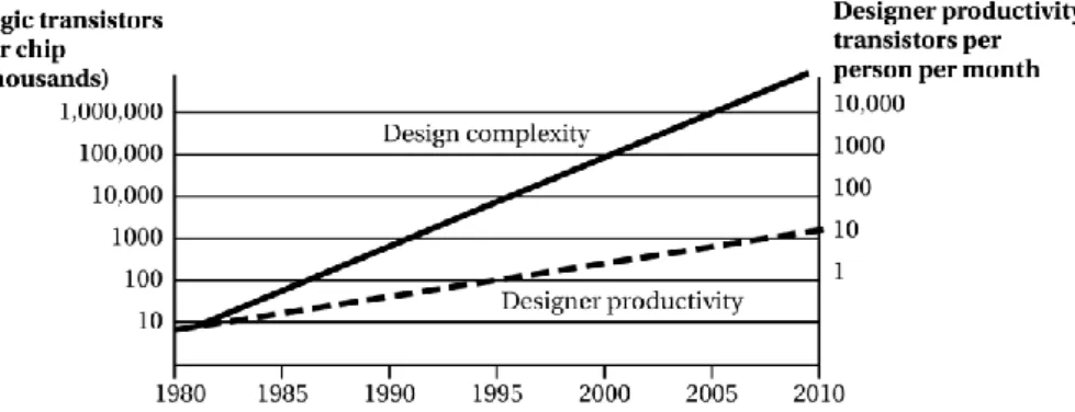
Methodologies: as estimated by SEMATECH, a consortium which performs research and development to advance chip manufacturing, design complexity presents a 58% annual increase in the number of transistors per chip, while the designer productivity grows by only 21% per year (see Figure 1.2). Embedded computing is one partial answer in order to overcome to this gap, since some of the design tasks are moved from hardware to software. However, improved design methodologies are required to deal with the increasing design complexity. Some of the methodology challenges are: to propose effective methods approaching the design by level of abstractions, to simplify the integration of functionalities composing the design and to favour the design reuse.
1.3 Next generation computing
Despite their great performance in terms of computational speed, power consumption and area, ASIC design paradigm undergoes huge limitations approaching billions of transistors designs. ASIC is a strongly application-oriented approach and as a consequence, when increasing designs complexity, it is characterized by lack of flexibility and reusability. Moreover, ASICs are susceptible to the rapid changes of consumer market across technology generations.
On the other hand, Digital Signal Processors (DSPs) and General Purpose Processors (GPPs) can offer relevant benefits in terms of flexibility though showing upper bounds on power supply voltage and clock frequency.
This aspect becomes an important issue especially considering the market trend where electronic devices for consumers represent a large percentage of the electronic request. This sector is mainly dominated by portable electronic devices for entertainment, communication, health & wellness, etc. Some examples are: smart phones, laptops & ultraportable computers, tablets, digital cameras, GPS navigators, multimedia devices, video game consoles, portable devices for fitness, diet & elder care. These devices are generally portable and although most of them offer very high performances in terms of processing, their success on the markets may be related to the battery
Figure 1.2. Design Complexity vs. Designer Productivity (Source: SEMATECH).
duration and other technical aspects.
Therefore, while power consumption and clock frequency issues cannot be ignored nor overcome, parallelization represents an interesting chance to deal with processing power. Multiple processing cores can be integrated in a single silicon chip offering higher computational power, and at the same time, avoiding the burden of a raising clock frequency, and hence a raising dynamic power consumption. This solution exploits the parallel computation based on many processing units (or cores) running at a lower frequency. This paradigm is also known as Multi Processor SoC (MPSoC). Examples are Intel Core Duo, i3, i5, i7 and Xeon, AMD Phenom II and FX, ARM Cortex-A9 or ARM11-MPCore.
Power consumption and frequency issues do not concern just portable devices, but they are starting to affect other sectors. This is due to an increasing common interest in caring energy utilization, together with emerging changes around computing requirements. Indeed, the wide diffusion of the Internet and its services, in particular the cloud computing, has caused processing loads to be transferred from the end-user to network providers. As a consequence of this scenario, on the one side users can enjoy a large amount of services saving local resources without suffering of portable devices limits. On the other side, service providers are in charge of answering a huge and time-variable request of computing resources.
Thus, recently market interest and research started focussing on low-power servers, thinking at more flexible architectures able to sustain high processing load peaks while reducing power consumption and avoiding power wastefulness during low processing load periods. Also in this scenario MPSoC architecture is definitely the most promising paradigm in terms of flexibility and power efficiency.
Furthermore, as discussed at the beginning of the chapter, according to the More-than-Moore trend, next generation of electronic devices will integrate multiple digital functionalities, non-digital computing, analog & mixed-signal processing, MEMS, RF components etc.
The design issues mentioned in the previous section suggest that the future computing design must be inspired on a flexible and reusable solutions able to face the raising design complexity and to meet time-to-market requirement. New design paradigms and methodologies, as well as advanced CADs are the key of the success for designer engineers in order to face new challenges of the computing design.
Finally, traditional on-chip buses represent the bottleneck on complex designs and in particular for parallel computing, so compromising the performance of the whole system. Network-on-Chip (NoC) is a promising methodology which allows designing of interconnecting architectures independently from the connected cores. The challenge in this case is to minimize the design effort while attempting to cover the widest application space in terms of traffic requirements (i.e. throughput, latency, quality of service, etc.) and implementation requirements (area, clocking scheme, and power consumption).
1.4 Application Domains
This section aims to figure out most promising application domains, trying to highlight opportunities and challenges. In particular, it is focused on healthcare domain. Many works can be found in the literature concerning the subjects dealt with in this section. In particular, the information discussed here mainly come from recent ITRS roadmaps and related reports [1]-[3].
Basically, the success of an application is based on a deep understanding of the societal needs and their relative trends, mixed to the ability to face them with simple, effective and attractive solutions.
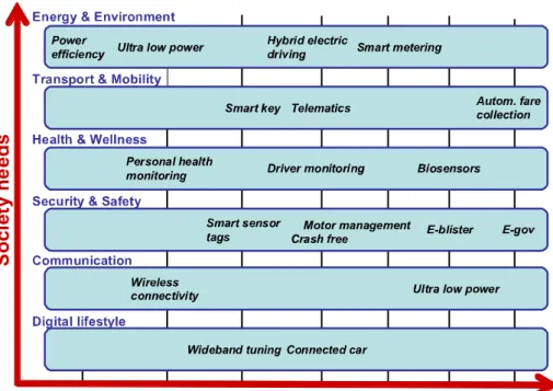
According to the ITRS indications, social trends can be mainly grouped into five categories:
energy & environment
transport & mobility
health & wellness
security & safety
communication & digital lifestyle
where the latter covers also consumer electronics for infotainment.
Each of these trends represents significant opportunities for future applications in the consumer electronics, automotive electronics, medical applications, communication, etc.
Figure 1.3 shows some examples of application linking societal trends and
markets.
Once focused on societal needs and trends, the following step is answering them with an innovative solution. Typically there are two main alternatives to corner the market.
The first one lies in the improvement of an existing solution. As for a portable consumer device, for example, this means improving its performance in terms of computational power, portability or battery duration. In some cases, the improvement is the result of crossing domains.
The second possibility consists in the introduction of a new solution opening a new market. For example, a bio-medical chip that may well revolutionize healthcare.
1.4.1 Healthcare
There is a wide consensus about the necessity of health monitoring application and Wireless Sensor Networks (WSN) as means to deliver higher quality health monitoring at lower cost. This general opinion is supported by many data, related to the high prevalence of certain chronic diseases and the ageing population in western countries. In fact, a large percentage of the total expenditure on health costs in Europe is spent on a few chronic diseases. Moreover, it is well known that the expenditure on healthcare will grow in the near future, because of an ageing population.
The use of health monitoring systems could result in more prevention and more on-line monitoring and this could rapidly reduce healthcare costs. Health monitoring devices can be divided into four main categories according to their application domains as follows:
Monitoring: it consists on a long-term collection of relevant data in order to allow the medical professional to make diagnosis.
Prevention: continuous monitoring of a known disorder in order to provide an alarm to detect and/or prevent the onset of the disorder. Prevention can also be used to assist in preventing the development of a disorder such as obesity, by monitoring the risk factors.
Closed loop: automatic detection of an adverse event, and automatic supplying outputs to overcome the adverse event.
Spot-check: whenever desired, the user can measure a body function.
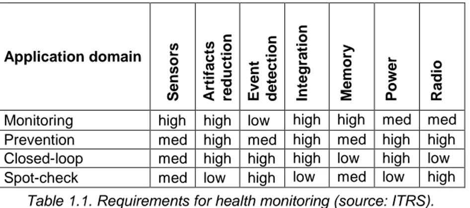
Most relevant elements composing a generic health monitoring system are the following:
sensors: appropriate sensors for accurately monitoring the relevant signals;
digital signal processing: providing intelligence for reducing artifacts and recognizing particular events;
integration technologies: combining electronics components in order to favour a suitably continuous monitoring;
memory: some applications use local storage of data, and therefore rely on the availability of memory;
power management: for autonomous devices, particularly relevant for portable and/or wearable devices;
radio technologies: for real-time monitoring and alerting, in order to transmit messages.
body/electronics interface: to capture the relevant body signals (i.e. electrodes with or without contact gel), and their corresponding
interfaces.
Table 1.1 gives a general indication about the influence of the monitoring health system components for each application domain.
Recent efforts on medical device development have focused on providing solutions for wearable health monitoring systems. The goal is allowing physiological monitoring and interpretation in daily life environments. However, some challenges are still to be faced. To provide these solutions, devices must be smaller and more comfortable to wear, be robust against motion artifacts, be power efficient, intelligent, and be able to communicate with the user.
Finally, today's interoperability and interconnectivity of these devices is ignored, resulting in limited monitoring functionality and limited intelligence achieved. Development of platform technologies towards wearable health monitors, may lead today’s limitations to be overcame.
1.5 Organization of this work
This work aims to give an overview on embedded computing design activities, taking into account two main viewpoints: the hardware level design and the application or system-level design. As discussed in this introduction, challenges and trends appear quite different for the two cases. While in the first case the research is mostly technology-driven, in the second case social needs are the main matter. However, the starting point in order to reach the greater success in future computing is a close collaboration between research domains, designers, industries and markets.
Chapter 2 represents an example of hardware level design. It introduces the design of a NoC interconnecting architecture for MPSoCs, based on high configurable building blocks, supporting advanced networking features directly implemented in hardware. In particular, the discussion focuses on a typical issue affecting complex designs: the configurability of a complex Intellectual Property (IP). This work proposes the Metacoding methodology and an
Application domain S enso rs Artif ac ts redu ctio n E ve n t d etect ion Int egra tion Me mo ry P o w er R adio
Monitoring high high low high high med med Prevention med high med high med high high Closed-loop med high high high low high low Spot-check med low high low med low high
automated design flow to overcome configuration issues. Without loss of generality, the methodology will be discussed referring to the particular case of the NoC building blocks.
Chapter 3 explores a couple of application designs dealing with remote monitoring platforms. At first, it introduces the design of a health monitoring system for patients affected by Chronic Heart Failure (CHF). This part discusses the main outcomes of the Health@Home (H@H) project which has been supported by the Ambient Assisted Living (AAL) programme. This project was successfully concluded with a demonstration over real CHF patients in three European hospitals. The chapter closes with a detailed state of the art for energy monitoring in Smart Grids and proposes an energy Home Area Network (HAN) based on Commercial Off the Shelf (COTS).
2
INTERCONNECTION ARCHITECTURES FOR
HETEROGENEOUS MPSOC: NETWORK ON-CHIP
A key element in Multi-Processor Systems-on-Chip (MPSoCs) is the global on-chip communication infrastructure, because its throughput, latency and power consumption set the limit to the overall performance.
The traditional shared bus approach exhibits its limits as the number of integrated IPs increases. Indeed, while gate delay scales with each new technology nodes, global wire delay increases and can be kept constant only by inserting repeaters [4]. For this reason shared bus communications standards are being substituted by multi-layer interconnects, now commonly referred to as Network-on-Chip (NoC). NoC is a scalable packet-switched communication infrastructures, connecting hundreds of IP cells, in MPSoC [5]-[28].
NoCs provide a methodology for designing an interconnect architecture independently from the connected cores that can be general purpose processors, Application Specific Instruction-set Processors (ASIP), Digital Signal Processors (DSP), memories or peripherals. Design flow parallelization, scalability and reusability all benefit from this approach [10]-[14], [29]-[49]. NoCs will be a key component also for the success of future 3D SoC [18], [19].
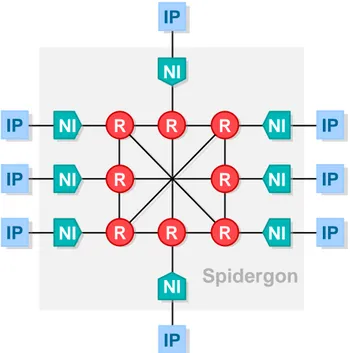
The NoC paradigm leverages the networking and parallel computing domain experience into the SoC world, implementing packet-switched micro-networks with an ISO/OSI like protocol stack. Examples of NoC architectures include Spidergon [13], [30], Mango [31], Aethereal [16], Arteris [32], Sonics [33], SoCbus [34] and xPipes [35], [36], [63].
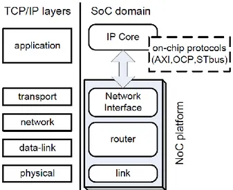
Figure 2.1. Typical ISO-OSI layers for Internet applications and their mapping onto NoC
Figure 2.1 illustrates the building blocks of a NoC and the corresponding layers in the ISO/OSI protocol stack. The Network Interface (NI) connects the cores to the NoC domain. The NI is made up of two separate components: shell and kernel. The shell encapsulates the transport layer and transforms local core transactions into NoC packets. The kernel implements the network layer and provides features such as data bus size and frequency conversion between the core and the NoC domain. By splitting transport and network layers into separate sub-components, plug & play design style is extremely simplified. The network is composed of a number of routers that pass packets between nodes. The router implements network and data-link layers. The physical link is responsible for actual signal propagation among routers and/or network interfaces.
For example, Figure 2.2 shows a NoC, based on Spidergon topology (a Ring one with an additional across link for each node to reduce network crossing latency), highlighting its hardware building blocks: connected IP cores, NIs, links and Routers (R) [20], [21], [25], [50].
Next sections are organized as follows. The Router architecture and features are described in Section 2.1. The core NI architecture is detailed in Section 2.2 while Section 2.3 illustrates the advanced NI networking features implemented. Section 2.4 introduces the Metacoding methodology and the automated design flow implemented to overcome configuration issues. Finally Section 2.5 collects some CMOS implementation results for different Router and NI configurations and a comparison with the state of the art.
Spidergon
IP
IP
IP
IP
IP
IP
IP
IP
IP
IP
IP
IP
IP
IP
IP
IP
NI
NI
NI
NI
NI
NI
NI
NI
NI
NI
NI
NI
R
R
R
R
R
R
R
R
R
R
R
R
R
R
R
R
NI
NI
NI
NI
2.1 Router Features and Architecture
The router proposed in this work features wormhole packet-switched routing with credit-based flow control and an arbitrary number of virtual channels. All router features are configurable at synthesis time, from arbitration policies to clocking schemes, for optimal trade-offs between network performance and physical design closure.
2.1.1 Topology and Routing
The router supports the Spidergon [13],[30] and ring topologies, plus a family of degree three topologies derived from Spidergon. The router is connected through two unidirectional links with three other routers in the network into directions Right, Left and Across, plus the fourth connection to the local Network Interface. When the Hierarchy link is instantiated, the router acts as a gateway between two NoC sub-networks (see Figure 2.3).
The router adopts the wormhole packet-switching technique, where a packet is subdivided into flits having their unique flow control. Once the first flit of a packet is routed, remaining flits follow the same path reserved to the header. This approach drastically reduces the amount of buffering (queues dimensioned with the granularity of a flit instead of a packet) and allows deeply pipelined data paths when compared to virtual cut-through and store & forward [44].
The routing algorithm is deterministic, so that always the same path is chosen between a source and a destination node, even if multiple paths exist. This choice avoids costly flit reordering at packet reception. The idea is to move clockwise or counterclockwise along the ring to reach destination nodes which are near the source node, and to use the Across link as first or last hop to jump to a part of the network that is far away from the source node.
The router uses a simple source-based routing: the entire path is encoded in the packet header, which has a fixed size due to the symmetry of the topology. This enables fast routing decision at each router, because the
RIGHT H IER AR CH Y LEFT A C R O S S N I L E F T AC RO SS RIGHT L E F T R I G H T ACROSS NI IP ROUTER ROUTER SUB-NETWORK NI IP N I ROUTER
information is simply extracted from the header, no computation or routing lookup table is required.
The router avoids end to end deadlocks by deploying Virtual Channels. Virtual Channels provide logical links over the same shared physical channels, by establishing a number of independently allocated flit buffers in the corresponding transmitter/receiver nodes. Typically, request and response Virtual Networks (VNs) are implemented on top of two disjoint Virtual Channels for sharing the physical link bandwidth and maximizing wire efficiency. The parametric number of Virtual Channels supported by the router can lead to advanced routing schemes or independent QoS traffic classes for real time and low latency flows.
2.1.2 Architecture
The router general architecture consists of the following main blocks, instantiated as many times as the number of links (see Figure 2.4):
Downstream Interface (DS ITF), which is connected to the input link and buffers incoming flits (separate Input Buffer for each Virtual Channel)
Routing Computation Unit (RCU), which extracts routing information from packets' headers
Switch, which routes inputs to outputs
Optional Output Queue (OQ) with bypass capability, which stores outgoing flits
OQ Arbiter, which arbitrates among different inputs requesting the same Output Queue. It is in charge of the per-packet allocation of the OQ, and so of the Virtual Channel
VN Arbiter, which arbitrates between the two Virtual Networks requesting link access. This is a per-flit arbitration, because the two packets of the two VNs can be interleaved on the link, depending on credits availability
Upstream Interface (US ITF), which is in charge of managing the credit-based output data flow
Downstream and Upstream Interfaces are dedicated components that implement the physical layer. The different links – synchronous or mesochronous [10] – correspond to different DS/US Interfaces instantiated in the router and in other NoC modules.
The above mentioned blocks can be grouped into DS-dependent blocks (DS Interface and RCU) and US-dependent blocks (Switch, Output Queue, OQ Arbiter, VN Arbiter and US Interface), as shown in Figure 2.4. DS-dependent blocks are instantiated for a link only if the corresponding DS interface exists; similarly, US-dependent blocks are instantiated for a link only if the corresponding US interface exists. The DS-dependent block of each link is connected to the US-dependent blocks of all the other links (represented in Figure 2.4 as crossed connections).
2.1.3 Buffering and Latency
The router adopts the credit-based flow control, which works on a flit per flit basis. Therefore, to guarantee the maximum link throughput, the Input Buffer is sized according to the credit round-trip delay. This delay can be defined as the minimum time between two consecutive credits for the same buffer location and it depends on the credit pipeline between two consecutive routers. The value of this delay is configurable, thus different design trade-offs in terms of working frequency and buffer resources are possible.
The router uses Output Queues for enhanced performance, avoiding head-of-line blocking. Queues are shared among input flows to limit costly time/space speed up factors and they have a bypass feature to reduce the router crossing latency in case of low traffic conditions. Output Queues are optional and are usually not instantiated in low cost (small footprint) implementations. It is optionally possible to implement a separate Output Queue for each input flow targeting a given output. This configuration improves the offloading capability of a router and it is particularly useful when multiple incoming heavy traffic streams target the same output port (typically the NI port).
The router has a configurable crossing latency, from one up to two clock cycles. This is obtained by means of a flexible pipeline in the data path: one stage is represented by the Input Buffer and the other stage is the optional output retiming register. The Output Queue, when instantiated, can be bypassed in case of low traffic conditions, thus not affecting the overall router
crossing latency. Registering input and output port signals allows orthogonality between the link and the router delay.
2.1.4 Quality of Service
QoS is based on the Fair Bandwidth Allocation mechanism. It allows for a flexible, scalable and low cost management of the allocation of the available bandwidth. The requested bandwidth value is programmed at the injection point (Network Interface) and is not explicitly linked to the path of a data flow through the router as it is done in other NoC architectures [31], [16]. The arbitration logic in the router is thus relatively simple, since it only requires a two-steps arbitration process based on the information available in the network header. When all data flows have the same bandwidth reservation, the arbitration degenerates into a Round Robin, Least Recently Used or fixed priority scheme. Speculation-like techniques allow the two arbitrations to be performed in parallel, thus reducing the critical path delay.
2.2 Core Network Interface Design
A key element of a NoC is the NI which allows IP macrocells to be connected to the on-chip communication backbone in a Plug-and-Play fashion. The NIs are the peripheral building blocks of the NoC, decoupling computation from communication. Basically, the NI is in charge of traffic packetization/depacketization to/from the NoC: it provides protocol abstraction by encoding in the packet's header all data to guarantee successful end to end data delivery between IP cores (transport layer) and all Quality of Service (QoS) information needed by the router at network layer. A NoC packet includes a header and a data payload which are physically split in units called flits. All flits of a packet are routed through the same path across the network. The header field is composed of both a Network Layer Header (NLH), whose content is determined by the NI according to the nodemap network configuration, and a Transport Layer Header (TLH) containing information used by the NIs for end-to-end transaction management.
Some NI designs proposed in literature also implement the conversion of data size, frequency and protocol between the original IP bus and the NoC. The IP bus can be a standardized one such as AMBA AXI (Advanced eXtensible Interface) [51] or OCP (Open Core Protocol) [52] or a custom bus, such STBus [53].
The latest research frontier on NI architecture design aims at integrating more features to directly support in hardware advanced networking functionalities. The challenge in doing so is keeping NI area, power and latency overheads as low as possible with respect to the connected IP cores.
In recent literature some NIs have been presented that add to the basic IP-NoC interface functionalities some features such as handling of out-of-order transactions in [51], [54], [55], detection of error transactions in [24], [56], secure memory access control in [57], QoS management and NI programmability in [58].
However, the literature does not present a design integrating all the abovementioned advanced features in the same NI with limited complexity overhead. With respect to the above NI functionalities other services may be
useful to support in hardware such as end-to-end interoperability between different IP bus types (e.g. end to end connection between an AXI IP core such as an ARM processor and a custom bus IP cell such as an ASIP or DSP coprocessor), management of pending transactions when powering down/up the IP to increase energy efficiency, remapping for master IP cores of their addressable NoC space. Particularly the interoperability feature is important since MPSoCs are often realized as the interconnection of heterogeneous IP cores provided by different vendors.
To overcome the limits of the state of the art this work presents the design and characterization in deep submicron CMOS technology of a NI architecture directly implementing in hardware advanced networking features such as: store&forward transmission, error management, power management, ordering handling, security, QoS management, programmability, interoperability, remapping. Such NI has been conceived as a scalable architecture: the advanced features can be added on top of a basic NI core implementing data packetization and conversion of protocols, frequency and data size between the connected IP core and the NoC. The NI can be configured to reach the desired trade-off between supported services and circuit complexity.
2.2.1 NI Top-level Architecture
IP cores in a NoC infrastructure are commonly classified into Master and Slave IPs: the former (e.g. a processing element) generates request transactions and receives responses, the latter (e.g. a memory) receives and elaborates the requests and then sends back proper responses. Initiator NIs are connected to Master IPs, and convert IP request transactions into NoC traffic, and translate the packets received from NoC into IP response transactions. Dually, Target NIs also exist, associated to Slave IPs. Target NIs present a mirrored architecture: requests are decoded from NoC; responses are encoded. In both NI types, two main domains can be identified (see Figure 2.5a referring to the top view of an Initiator NI and Figure 2.5b referring to the top view of a Target NI): the Shell, IP specific, and the Kernel, NoC specific, each one having its own peculiar functionality and interface.
Figure 2.5 highlight also some advanced networking features such as programming, security, error and power management detailed in Section 0. The aim of the Shell/Kernel separation is to abstract IP specific properties (such as bus protocol and data size) from NoC side properties. This way the NoC becomes an IP-protocol agnostic interconnect, that is whichever protocol, bus size, clock frequency the Master or Slave IP is using, all modules in the system may communicate with each other.
Conversion features must be implemented in the two directions, called request path (from Master to Slave IPs, blue paths in Figure 2.5) and response path (from Slave to Master IPs, red paths in Figure 2.5) respectively. While the Kernel, and the associated NoC interface, is IP protocol independent and its design is common to all possible NIs, the Shell needs to be defined on a per-protocol basis. A specific Shell architectural design is needed for each IP protocol that must be connected to the NoC. The proposed NI supports the following IP bus protocols: AMBA AXI, a de-facto standard in embedded systems; STBus TYPE 3 [53] used by STMicroelectronics as the backbone of its SoC designs; DNP, a distributed network processor interface developed within the SHAPES European Project [5], [6], [10], including STMicroelectronics and ATMEL as main industrial partners, to build a multi-tile MPSoC architecture. In case the programming interface feature is activated, the STBus TYPE 1 or the AMBA APB bus are used as programming bus.
IP
protocol
Shell
Handshake IP protocol Encode/Decode IP protocol Programming Security accessKernel
NoC packet assembling/ disassemblingData size & Frequency conversion Error management
E
rr
or M
an. U
nit
NoC Int
e
rfa
c
e
NoC
packets
(a) Initiator NoC packetsNo
C I
n
te
rfa
c
e
Err
o
r M
an
.
U
n
it
Kernel
NoC packet assembling/ disassemblingData size & Frequency conversion Error/Power management
Shell
Handshake IP protocol Encode/Decode IP protocol Programming IP protocol (b) TargetFigure 2.6 provides a more detailed insight of the core NI Initiator architecture with a clear distinction between request and response paths. Advanced functionalities, whose implementation is described in Section 2.3, will be added on top of this core NI architecture. From left to right, Figure 2.6 highlights the Shell, the Kernel and the NoC interface respectively. Moreover, the top of the figure refers to the request path, while the bottom part refers to the response path. The NoC interface presents an Upstream (US) section, to send packets to the NoC, and a Downstream (DS) section, receiving packets from the NoC.
The NI Shell part deals directly with the bus protocol, implementing bus specific handshaking rules by means of dedicated Finite State Machines (FSMs). Before passing data on to the Kernel, the Shell also builds the Network and Transport Layer headers, needed by subsequent NoC components (i.e., routers and target NIs) for forwarding the packet and decoding it at destination. The NI Kernel part manages buffering and other services (described in Section 2.2.2) in an IP-protocol independent way.
2.2.2 Kernel-Shell Interface by Bi-synchronous FIFOs
The Kernel is interfaced to the Shell by means of a FIFO-like interface. As reported in Figure 2.6, encoded data coming from the Shell are stored in two FIFOs, an header FIFO (holding transport layer and network layer headers)
Header Decoder Header Decoder Response Output FSM Response Output FSM Payload FIFO Payload FIFO Header Read Manager Header Read Manager Response Input FSM Response Input FSM Header Write Manager Header Write Manager Payload Read Manager Payload Read Manager Payload Write Manager Payload Write Manager Header FIFO Header FIFO Bus data Header FIFO Interface Bu s Int er fac e TLH Encoder TLH Encoder Request Input FSM Request Input FSM Payload FIFO Payload FIFO Header Write Manager Header Write Manager Request Output FSM Request Output FSM NLH Encoder NLH Encoder Header Read Manager Header Read Manager Payload Write Manager Payload Write Manager Payload Read Manager Payload Read Manager Header FIFO Header FIFO
Bus data & Byte enable Header FIFO Interface Bu s Int er fac e Shell Kernel NoC US Interface NoC US Interface NoC DS Interface NoC DS Interface No C Int er fac e Interface No C Int er fac e Reque s t path Re s ponse path
and a payload FIFO (holding bus raw data). Each FIFO has its own read and write managers which update FIFO pointers and status, and provide frequency conversion mechanisms. The Kernel is connected to the NoC interface stage through two additional FSMs. In the request path, an output FSM (OFSM) reads headers and payloads and converts them into packets according to the NoC protocol. In the response path, an input FSM (IFSM) collects packets and splits header and payload flits into their respective FIFOs. To be noted that the NI encodes both the TLH and the NLH, while in the decoding action only the TLH is taken into account because the packet has reached its destination and routing data are not needed.
By using bi-synchronous FIFOs in the NI scheme of Figure 2.6 frequency conversion is accomplished between NoC and each connected IP. Each read (write) FIFO manager re-synchronizes in its own clock domain the pointer of the write (read) manager in the other clock domain. Hence, the empty/full status of the FIFO is known by comparison of synchronized pointers, and the header or payload FIFOs can be correctly managed. To increase the robustness of the synchronization the pointers adopt a Gray encoding. Normally, this would limit the possible FIFO sizes to powers of 2, but thanks to a user-transparent pointers initialization any even number of locations can be supported. To be noted that vs. other works in literature [59] that synchronize different clocks but with the limit of an integer ratio between the frequencies, our bi-synchronous FIFO can handle arbitrary ratio clocks.
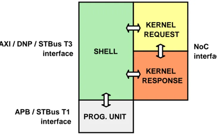
Figure 2.7 highlights the different four clock domains that can be supported in the proposed NI architecture.
As shown in Figure 2.8, since read (RD) and write (WR) managers can access a FIFO by different basic storage units, also data size conversion between IP and NoC domain is possible. The conversion is managed by exploiting FIFO rows and columns concepts. A FIFO location, or column, is sized according to the larger data size between data in and data out; a FIFO row is sized according to the smaller data size between data in and data out. Up-size conversion is accomplished by writing by rows and reading by
NoC interface AXI / DNP / STBus T3 interface SHELL KERNEL REQUEST PROG. UNIT KERNEL RESPONSE APB / STBus T1 interface
Figure 2.7. Clock domains in the proposed NI architecture.
columns; down-size conversion is exactly the opposite. For example, consider large opcode store operations (i.e., with large amount of payload data) generated by an IP with data bus size of 32 bits and connected to a NoC with flit size of 128 bits (up-size conversion): four 32-bit data write accesses by the IP are necessary to fill a 128-bit payload FIFO location and make it available to the NoC to read it (see Figure 2.8, focusing on a single 6-location FIFO). In particular conditions when no size conversion nor Shell/Kernel frequency conversion is needed, nor Store & Forward support is required, it is possible to remove the bisynchronous FIFOs, by setting their size to zero, thus saving area and power consumption. This feature is known as Zero-FIFO Kernel. As far as the NI crossing latency is concerned, its minimum value depends on the pipeline stages used. Typically, at least one retiming is performed due to the presence of the FIFO in the Kernel (unless the Zero-FIFO Kernel feature is enabled). To increase the maximum operating clock frequency, optional pipeline stages can be added at the IP and NoC interfaces. Thus, a maximum of three retiming stages can be implemented. Obviously, the minimum NI crossing latency is equal to the number of retiming stages instantiated, but its actual value may be increased by other factors: for example, in case of frequency conversion the synchronization delay has to be added; or if the current IP traffic has a low priority the NoC QoS support may slow down its access to the interconnect, or the store&forward mechanism (see Section 2.3.1) might be enabled, thus increasing the traffic latency.
2.2.3 NI Physical Link and NoC Interface
As far as the physical link is concerned, at the NoC interface side there are the following hardwired lines for each response or request path, see Figure 2.9:
N-bit flits used to transfer NoC packets (headers and payloads), with N configurable at synthesis time;
4-bit flit_id, whose 2 LSBs identify first, intermediate and last flits of a packet; the flit can also be a single one. Other optional bits of this signal are used to mark the end of bus packets within compound
transactions (i.e. composed of a number of packets) that are translated into a single NoC packet, and to identify payload flits that cannot be aggregated in case of upsize conversion (necessary in some cases of interoperability);
the optional K-bit four_be (K=N/32) to mark meaningful 32-bit pieces of data within a flit and used in end-to-end size conversion.
the optional 2-bit flit_id_error for signalling a slave side error or an interconnect error;
the optional flit_id_atomic which enables support of atomic operations: a NI can lock paths towards a Slave IP so that a Master IP can perform a generic number of consecutive operations without any interference from other masters;
credit and valid signals for credit-based flow control. A flit is sent only when there is room enough to receive it: neither retransmission nor flit dropping are allowed. This is done automatically by setting an initial number of credits in the US interface (in its Credit Manager), equal to the size of the Input Buffer in the DS interface it communicates with. Since the US interface sends flits only if the connected DS interface can accept them, there are no pending flits on the link wires. This approach allows virtual channel flit-level interleaving, so that separate virtual networks can share the same physical link. See Section 2.3.7 for more details on Virtual Networks.
NoC Module flit flit_id flit_id_error flit_id_atomic four_be valid credit NoC US Interface Credit Manager NoC Module NoC DS Interface Input Buffer
2.3 Advanced Network Interface Features
The next sub-sections describe the configurable services available as special features in the novel NI design, and patent filed in US and Europe. Figure 2.10 highlights some of the additional configurable features on a NI initiator. The proposed design is the first in literature directly implementing in hardware all advanced networking features: store & forward transmissions, error management, power management, security, ordering handling, QoS management, programmability, interoperability, remapping.
2.3.1 Store & Forward (S&F)
Kernel FIFOs in both Request and Response paths contain flits, either received from the NoC and to be decoded towards the IP bus, or encoded from a bus transaction and to be transmitted over the interconnect. Default NI behaviour is that a flit is extracted from the FIFO as soon as it is available. Hence, if the original traffic at an interface (NoC or bus) has an irregular nature, such a shape is reflected also into the other interface (bus or NoC).
Header Decoder Header Decoder Response Output FSM Response Output FSM Bus data Header Bus In te rfac e TLH Encoder TLH Encoder Request Input FSM Request Input FSM NLH Encoder NLH Encoder
Bus data & Byte enable Header Bus In te rfac e Shell
Shell KernelKernel
Reque s t path Reque s t path Re s ponse path Re s ponse path Security Security Ordering handler Ordering handler Reti m in g St a ge Reti m in g St a ge Programming Interface Programming
Interface RegistersRegisters
Progra m m in g Bus Reti m in g St a ge Reti m in g St a ge