Autore:
Michele Dei
Relatori:
Prof. Paolo Bruschi
Ing. Massimo Piotto
Prof. Andrea Nannini
DESIGN OF SMART SENSORS FOR
DETECTION OF PHYSICAL QUANTITIES
Anno 2010
UNIVERSITÀ DI PISA
Scuola di Dottorato in Ingegneria “Leonardo da Vinci”
Corso di Dottorato di Ricerca in
Ingegneria dell’Informazione
ABSTRACT
Microsystems and integrated smart sensors represent a flourishing business thanks to the manifold benefits of these devices with respect to their respective macroscopic counterparts. Miniaturization to micrometric scale is a turning point to obtain high sensitive and reliable devices with enhanced spatial and temporal resolution. Power consumption compatible with battery operated systems, and reduced cost per device are also pivotal for their success. All these characteristics make investigation on this filed very active nowadays.
This thesis work is focused on two main themes: (i) design and development of a single chip smart flow-meter; (ii) design and development of readout interfaces for capacitive micro-electro-mechanical-systems (MEMS) based on capacitance to pulse width modulation conversion.
High sensitivity integrated smart sensors for detecting very small flow rates of both gases and liquids aiming to fulfil emerging demands for this kind of devices in the industrial to environmental and medical applications. On the other hand, the prototyping of such sensor is a multidisciplinary activity involving the study of thermal and fluid dynamic phenomenon that have to be considered to obtain a correct design. Design, assisted by finite elements CAD tools, and fabrication of the sensing structures using features of a standard CMOS process is discussed in the first chapter. The packaging of fluidic sensors issue is also illustrated as it has a great importance on the overall sensor performances. The package is charged to allow optimal interaction between fluids and the sensors and protecting the latter from the external environment. As miniaturized structures allows a great spatial resolution, it is extremely challenging to fabricate low cost packages for multiple flow rate measurements on the same chip. As a final point, a compact anemometer prototype, usable for wireless sensor network nodes, is described.
The design of the full custom circuitry for signal extraction and conditioning is coped in the second chapter, where insights into the design methods are given for analog basic building blocks such as amplifiers, transconductors, filters, multipliers, current drivers. A big effort has been put to find reusable design guidelines and trade-offs applicable to different design cases. This kind of rational design enabled the implementation of complex and flexible functionalities making the interface circuits able to interact both with on chip sensors and external sensors.
In the third chapter, the chip floor-plan designed in the STMicroelectronics BCD6s process of the entire smart flow sensor formed by the sensing structures and the readout electronics is presented. Some preliminary tests are also covered here. Finally design and implementation of very low power interfaces for typical MEMS capacitive sensors (accelerometers, gyroscopes, pressure sensors, angular displacement and chemical species sensors) is discussed. Very original circuital topologies, based on chopper modulation technique, will be illustrated. A prototype, designed within a joint research activity is presented. Measured performances spurred the investigation of new techniques to enhance precision and accuracy capabilities of the interface.
A brief introduction to the design of active pixel sensors interface for hybrid CMOS imagers is sketched in the appendix as a preliminary study done during an internship in the CNM-IMB institute of Barcelona.
TABLE OF CONTENTS
CHAPTER 1:
DESING AND DEVELOPMENT OF INTEGRATED THERMAL SENSORS
FOR GAS AND LIQUID FLOW SENSING ...1
1.1 MEMS and integration technology ...1
1.2 Integrated flow-meters ...2
1.2.1. Mechanical flow sensors...3
1.2.2. Thermal flow sensors ...4
1.3 Design of an integrated calorimetric flow-meter ...8
1.3.1. Differential calorimetric flow sensor in the
BCD6 processes of STMicroelectronics...9
1.3.2. Packaging methods for integrated
thermal flow sensors...12
1.3.3. Design of thermal flow meter by means
of FEM simulations ...17
1.3.4. Open loop compensation for sensor structural offset ...22
1.3.5. Heat losses through suspending arms ...27
1.3.6. Low pressure effects on miniaturized
thermal flow-meters ...28
1.4 A CMOS compatible flow-meter for liquids ...32
1.5 Prototype of a double channel flow-meter on a single chip...36
1.5.1. Fluid-dynamic simulation of the velocity profile ...42
CHAPTER 2:
INTERFACE ELECTRONICS FOR INTEGRATED THERMAL
FLOW-METERS ...49
2.1 Requirements and sensor electrical characteristics...49
2.2 Design of CMOS chopper amplifiers for thermal sensor interfacing .50
2.2.1. Instrumentation amplifier topology and analysis...53
2.2.2. Design of the prototype...55
2.3 Gm-C biquadratic cells for chopper amplifier band limiting...58
2.3.1. Gm-C biquad architecture for low pass filtering...58
2.3.2. Linear transconductor for low frequency operation
(version 1) ...61
2.3.3. Linear transconductor for low frequency operation
(version 2) ...63
2.3.4. Simulated performances of the redesigned Gm-C filter ...66
2.4 Sensor driving circuits and pressure effects compensation
loop...68
2.4.1. Implementation of the common mode amplification chain ...74
2.4.2. Digitally controlled current driver...78
2.4.3. Full-analog CMOS current driver ...80
2.4.4. Four quadrant multiplier based on current divider cells ...86
CHAPTER 3:
DESIGN OF A SMART CHIP PROTOTYPE FOR INTEGRATED
THERMAL FLOW-METERS ...91
3.1 Electronic blocks and auxiliary circuits ...91
3.1.1. On chip clock generation ...93
3.1.2. Controlled heating of the chip ...96
3.1.3. Differential mode readout chain ...98
3.1.4. Common mode readout chain...100
3.1.5. Digital communication interface ...100
3.2 Chip layout...104
3.2.1. Sensors layout...104
3.2.2. Pad frame...105
CHAPTER 4:
DESIGN OF LOW POWER INTEGRATED INTERFACES FOR
CAPACITIVE SENSORS ...113
4.1 Integrated capacitive sensing...113
4.1.1. Capacitive sensors ...113
4.1.2. Integrated interfaces for capacitive sensing ...116
4.2 Capacitive to PWM signal converters...120
4.2.1. C-to-PWM converter ...120
4.2.2. Prototype of a capacitance to voltage converter ...128
4.3 Improvements to the C-to-PWM interface ...131
4.3.1. Double clock technique for dynamic range extension ...131
4.3.2. Dynamic matching of C-to-PWM input ports ...141
CONCLUSIONS ...145
APPENDIX:
DESIGN OF PIXEL SENSORS INTERFACE FOR HYBRID CMOS
IMAGERS ...147
A.1 Fast infrared imager ...147
A.2 Address-Event Representation (AER) ...148
A.3 Pixel interface electronics...149
A.4 Arbitration...151
1. DESING AND DEVELOPMENT OF INTEGRATED THERMAL
SENSORS FOR GAS AND LIQUID FLOW SENSING
1.1 MEMS and integration technology
Since Feynman's challenge in the famous lecture in 1959 [1], a great effort has been put in technology research to master micrometer scale and nanometer scale physics in order build sophisticated devices. Micro-electro mechanical systems (MEMS) belong to that class of devices, and, nowadays MEMS market represents a profitable and prominent field in electronic industry, with a projection of increasing leverage in the following years [2].
Their remarkable economical impact, commented in Fig.1.1 have been achieved, so far, thanks to consumer electronics products, such as game controllers, digital cameras, camcorders, MP3 players, personal navigation devices etc. At the same time the word “MEMS” begins to be part of common spoken language thanks to frequent articles in daily newspapers regarding MEMS tailored to more and more specialized applications (flying micro-robots, smart dust, wearable computers and silicon micro-surgery).
MEMS technology initially developed from the well consolidate IC technology, using the same technological procedures such as: deposition, epitaxy, thermal oxidation, implantation, sputtering, casting, etching where layers are patterned using photo-lithography, inheriting one of the most important aspects of economical success: the possibility of batch fabrication techniques similar to those used for integrated circuits. Furthermore possibility to integrate these electromechanical elements together with electronics allows the implementation of a system able to
Fig. 1.1 – Ranking of companies in the global consumer/mobile MEMS market in 2008. Data are taken from [2]. The market forecast society iSuppli predicts that MEMS market will increase to 2.4 billion dollars in 2012, up from scarcely 1 billion dollars in 2006.
accomplish complex functionalities, usually referred to as system-on-a-chip.
Anyway it should be also pointed out that MEMS technology is not solely about making things out of silicon; nowadays MEMS technology evolves and includes also non-standard techniques in IC processing such as anodization, or Silicon-Germanium deposition in order to strive for new applications and/or better performances. The term micromachining is referred, in this respect, to all the techniques used to fabricate MEMS.
On the other hand, the term MEMS, in a strict sense, depicts a micron scale transducer device that links mechanical and electrical quantities. Anyway, it has become common to indicate with MEMS all sort of micron scale devices which are able to detect or to perturb same kind of physical quantity (mechanical, thermal, biological, chemical, optical, and magnetic phenomena) producing an electrical signal or controlled by an electrical signal. These two functions can be accomplished by MEMS sensors or MEMS actuators, respectively.
1.2 Integrated flow-meters
Dealing with a flow of fluid can be misleading unless the issue of physical quantities is not clarified: a fluid flow can be either a gas flow or a liquid flow. Among others quantities, a fluid flow can be measured in terms of amount of moved mass (weight per unit time), moved distance (meters per unit time), moved volume (volume per unit time). Anyway in this work we will consider preferably two principal units of measurement: the standard cube centimer per minute (sccm), when dealing with gasses, and the milliliter per minute (ml/min) when dealing with liquids.
A variety of conventional macroscopic flow sensors exist, but they are often of little use in the micro domain. Limited sensitivity, large size and high dead volume restrict their use for some specific applications, especially in the very low flow regimes. On the other hand, microfabricated devices offer the benefits of high spatial resolution, fast time response, integrated signal processing, and potentially low costs. A crucial issue is power consumption especially when aiming to battery-powered systems: in this respect, micro-scale flow meters typically outperform the macroscopic counterpart. They have recently matured from the research stage to commercial applications (see for example: Sensirion AG, Honeywell, Bosch, SLS Micro Technology) and are now real competitors for conventional sensors.
The automotive industry has been, and is still one of the major driving forces for MEMS-based sensors. In the last years the number of sensors in engine control applications, is constantly increasing [3]. Micro flow-meters are essential in the electronic fuel injection systems where it is needed to know the mass flow rate of air sucked into the cylinders to meter the correct amount of fuel [3–5].
Other areas of application are in pneumatics, bioanalysis [6], metrology (wind velocity and direction [7, 8]), civil engineering (wind forces on building), the transport and process industry (fluidic transport of media, combustion, and vehicle performance), environmental sciences (dispersion of pollution), medical technology (respiration and blood flow, surgical tools [9]), indoor climate control (ventilation and air conditioning [10]), and home appliances (vacuum cleaners, air dryers, fan heaters). Due to their very small pay-load, integrated flow sensors represent a optimal alternative also in space applications: they have been yet used as within
measuring instruments for space scientific experiments and control the mass of propellant expulsed by thrusters.
The first micromachined flow sensors were presented by van Putten et al. [11] and van Riet et al. [12] in 1974. They used the thermal domain as the measurement principle. In principle, a large variety of physical principles other then thermal can be used to detect fluid flows, but most of them are not suitable for integration. In this respect, thermal flow-meters are to be preferred for their mechanical simplicity, absence of moving parts, high sensitivity and relative robustness.
In the next sessions we will briefly review some mechanical flow sensors and than we will illustrate the more popular thermal flow sensors. More sophisticated (and complicated) revealing methods, such as Coriolis force sensors, fluid imaging and optical flow sensing are not covered here and are beyond the aim of this thesis. The interested reader can find more on these topics in references [13, 14].
1.2.1. Mechanical flow sensors
Sensing of a flow rate can be achieved through electro-mechanical transduction of the forces of the fluid applied to a solid element. Although a lot of different and sophisticated methods of interaction between the fluid and a solid body can be exploited, in principle, to the sensing purpose, some of them are impracticable for integration at the micron range scales. Here, we resume some of the most popular types of mechanical flow sensors: (i) pressure difference sensors, (ii) drag force sensors and (iii) lift force sensors.
Pressure difference sensors rely on the measurement of the differential pressure P in a flowing fluid. Pressure sensors can be used to measure flow by sampling the pressure drop along a flow channel with known fluidic resistance, Rf, and calculating the flow Q from the fluidic equivalent to Ohm’s law: Q = ∆p/Rf. It is comparable to measuring the current (Q) in an electric circuit by sensing the voltage drop (∆p) over a fixed resistance (Rf).
Inlet Outlet p1 p2 Glass Silicon Flow restriction p1 p2 (a) (b) Silicon Piezoresistor Sensor diaphragm Orifice p1 p2 Flow (c)
Fig. 1.2 – Pressure Difference sensors for flow measurements. Pressure difference ∆p = p2 – p1 is transformed into electrical signal using:
Figure 1.2 shows three possible implementations of this technique. More details on capacitive sensors will be given in chapter 4 of this thesis. It is important to point out that all this kind of sensors needs to create a flow restriction in order to make Rf high enough and to produce a measurable pressure drop ∆p across the channel. This represents an important flaw in many applications, such as anemometry for example, where little insertion pressure lost is desired.
On the other hand, drag and lift force flow sensor consists of a cantilever beam, or paddle, with an integrated strain gauge resistor. When the cantilever is immersed in a flowing fluid, a drag force is exerted resulting in a deflection of the cantilever, which can be detected by the piezoresistive elements incorporated in the beam. Figure 1.3(a,b,c) shows schematics of devices using this measurement principle. A general disadvantage of the drag force flow sensors is the possible damage through high-speed particles, which can destroy the petit paddle suspension, or low-speed particles, which clog the fluid pathway and block the paddle in case of in-plane sensor arrangement. There is a trade-off between robustness and
sensitivity of the sensor. However, the chip size is generally smaller than the pressure difference flow sensors. These sensors, like the pressure difference sensor of the preceding section, do not induce heat to the fluid, which could represent an advantage in some applications.
1.2.2. Thermal flow sensors
Integrated thermal flow sensors fabricated through micromachining technology present, respect to the mechanical counterpart, structural and electronic simplicity. Furthermore it has been largely demonstrated that it is possible to get high
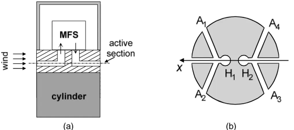
Flow Wind receptor hair
Strain gauge
(a) (b)
(c)
Fig. 1.3 – Examples of force driven flow sensors: (a) in-plane drag force flow sensor, (b) out-of-plane drag force flow sensor, (c) lift force sensor.
performance sensor starting from standard CMOS IC process and adding some post-CMOS micromachining and/or some deposition technique [15]. For this reason, the overwhelming majority of micro flow sensors work in the thermal domain. In this respect we have to point out some requirements of CMOS solid-state sensors:
i. Use the materials provided by the CMOS IC process. ii. Exploit the thermal (and coupling) effects inherent in the
CMOS materials.
iii. Design structures that bring out the transducer effects, but within the limits of the CMOS and post-CMOS fabrication rules (which are broader than the conventional CMOS IC design rules).
CMOS materials include bulk silicon, polysilicon (possibly both n- and p-doped), dielectrics (silicon oxide, silicon nitride, passivation), and metal (alloy with mainly aluminium). All these materials can serve as thermal mass. Silicon and metal conduct heat efficiently. The dielectric layers provide only moderate thermal isolation in view of their small thicknesses. That is why removal of material by micromachining is required for efficient thermal isolation.
The thermoresistive effect (Joule heating) makes it possible to use electrically conducting materials, such as polysilicon, for resistive heating which is the base for every thermal flow-meter. The temperature coefficient of resistivity is exploited for resistive thermometers: RTD and thermistors. The difference in Seebeck coefficients between different conducting CMOS materials (including differently doped silicon areas) is the basis of integrated thermocouples and thermopiles that will be illustrated at the end of this section. Finally, the different thermal expansion coefficients of different CMOS materials produce the bimorph effect, which can be exploited for the thermo-mechanical actuation of micromechanical structures. All these thermal properties depend on doping and structure (mono- or polycrystalline) and as a consequence they heavily depend on the process. For example, the temperature coefficient of the resistivity of polysilicon can be positive or negative, depending on doping. Besides, sheet resistance, resistive temperature coefficients, major carrier density (n or p for semiconducting materials), Seebeck coefficients, temperature conductivity and specific heat represent the basis for thermal MEMS design. All of these properties are temperature dependent. Thermal flow sensors can be classified into three basic categories, schematically sketched in Fig. 1.4:
(a) Hot wire/hot film anemometers: they are thermal mass flow sensors which measure the effect of the flowing fluid on a hot body.
(b) Calorimetric flow sensors: they are thermal mass flow sensors which measure the asymmetry of temperature profile around the heater which is modulated by the fluid flow.
(c) Time of flight sensors: they are thermal mass flow sensors which measure the passage of time of heat pulse over a known distance.
Hot wire/hot film anemometers exploit the effects of thermal conductance variation due to the fluid in motion. An ideal anemometer, i.e. with no heat losses on supports, obeys to the King’s law:
v G
v
GT( )= T(0) 1+β (1.1)
Where GT(v) is the total thermal conductance seen by the wire/film as function of the flow velocity v, while β is a coefficient dependent by the fluid characteristics and the geometries of the sensor, usually empirically determined.
A micromachined anemometer is often formed by a suspended dielectric cantilever (hot wire) or membrane (hot film), while usually the sensing element is a patterned layer of platinum. Other materials can be used such as gold, polysilicon, and amorphous germanium; anyway platinum is the best choice in terms of chemical stability with temperature. The wire/film is driven to a temperature higher than the fluid temperature, justifying the name hot wire/film. The motion of the fluid forces a heat loss of the sensor as the total thermal conductance changes with eq. (1.1). On the other hand, a temperature change influences the electrical conductivity of the wire/film offering the possibility to detect the fluid velocity through the relative electrical resistance variation. This technique can exploit the so called RTD (resistive temperature detector) devices.
The calorimetric principle illustrated in Fig. 1.4(b). For such arrangement, the heat source and the temperature probes are distinct and can be bipolar transistors, field
(a)
(b)
(c)
Fig. 1.4 – Schematic of the working principles of thermal flow sensors: (a) anemometer (heat loss), (b) calorimetric flow sensors (thermotransfer),
effect transistors or even diodes: all this devices offers a relevant sensitivity to temperature changes. Differently when used as pure electronic devices, high temperature sensitivity represents a good advantage here. Anyway, in order to obtain effective temperature isolation from the silicon substrate, large area of the chip has to be suspended and considerable technological difficulties arise.
The sensors presented in this thesis are based on a different thermal to electrical conversion principle, known as Seebeck effect, which is a reversible thermo-electrical phenomenon occurring when two jointed thermo-electrical conducting materials (metals or semiconductors) are submitted under a thermal gradient. In Fig. 1.5 a schematic representation is given, where the conductors A and B are jointed in two points each of them at a fixed temperature forming a so called thermocouple. The circuit has broken by the insertion of an ideal voltmeter which reveals a voltage difference ∆V.
The differential Seebeck coefficient (also called thermopower) is defined by: = → T V T AB ∆ ∆ α ∆lim0 . (1.2)
The coefficient αAB is a function with the absolute temperature and is determined by the chosen couple of conductors A and B. It can be expressed by two distinct coefficients, αA and αB, called absolute thermopower of A and B, respectively:
B A
AB α α
α = − . (1.3)
Seebeck coefficients of materials available in standard CMOS processes do not come through the few microvolt per centigrade. Typically thermocouples are electrically connected series in order to form a thermopile. A thermopile formed by N equal thermocouples, with all hot junctions well thermally coupled and all the cold junctions thermally coupled, present a global Seebeck coefficient equal to:
LE THERMOCOUP THERMOPILE N α
α = ⋅ . (1.4)
In the next section we will illustrate more deeply the sensors used in this work that are based on the Bipolar-CMOS-DMOS version 6 (BCD6) process of STMicroelectronics.
Fig. 1.5 – Schematic representation of a thermocouple. A and B are two conducting materials, V is an ideal voltmeter. Junctions are subjected to two different temperatures: the junction at T + ∆T is called hot junction, while the
1.3 Design of an integrated calorimetric flow meter
Sensing principles described in Fig. 1.4 apply also for macroscopic thermal flow sensors. When dealing with micron scale silicon structures the problem of thermal insulation has to be coped, as all thermal sensing principles are based on the presence of some on temperature difference. Unfortunately, the high thermal conductivity of bulk silicon prevents the chip from large temperature gradients. Typically, a micromachining technological step is needed to obtain the suspension of hot elements in order to realize a physical separation of the latter with respect to the bulk. Once solved this technological problem, the integrated structures takes a substantial advantage with respect to the macroscopic thermal flow sensors in terms of:
(i) Speed, as it increase with the second power of typical geometrical features of the sensor; this can be qualitatively demonstrated considering, under small Biot number hypothesis, the thermal time constant RC is given by R = L/(k·A), C = CP·L·A, where L is the length along heat exchange direction, A is the respective cross section, while k and CP are the thermal conductivity and the specific heat at constant pressure of the material.
(ii) Power consumption, as very small thermal masses have to be heated.
(iii) Miniaturization, obviously. It is worth noting that miniaturization has a potential impact on sensor sensitivity, because the sensor can be introduced in very small cross section channels, allowing very low mass flows to be measured.
In a typical standard CMOS process the usable materials for the temperature sensing structures are: aluminium metal layers, polysilicon (n and p), unsiliced and silicided polysilicon. With these layers, it is possible to implement both thermisors and thermopiles. Until now an analytical comparison in presence of other constraints, such as dissipated power and area occupation, has not been done to the author knowing, anyway generally integrated thermistors are considered to be more sensitive with respect to integrated thermopiles. For example typical values for a n+polysilicon/p+polysilicon thermocouple are about 400 µV/K, while for for a n+polysilicon/aluminium thermocouple, values are stated below 100 µV/K; the temperature coefficient of resistance (TCR ≡ ∆R/R·1/T) of a polysilicon strip can reach up to 0.5 %/K.
On the other hand, thermopiles are offset-free temperature sensors, as for ∆T = 0 their output voltage is intrinsically zero, while thermistors have to be connected in a Wheatstone bridge configuration which inevitably results unbalanced due to device mismatching, and an accurate and reiterated in time calibration/trimming is needed. Furthermore offset may result temperature dependent, and, as the operative temperature vary with the applied flow, heavy limitation of measure accuracy has to be expected. For this reasons, the work presented in this thesis is focused on thermopile based calorimetric sensors.
1.3.1. Differential calorimetric flow sensor in the BCD6 process of
STMicroelectronics
The sensing structure shown in Fig. 1.6 represents a classical differential calorimetric flow-meter made up of a heater placed between an upstream and a downstream temperature probe placed symmetrically with respect to the heater. The actual sensor made out on the STMicroelectronics BCD6 process counts with a 1 kΩ polysilicon resistor, constituting the heater, positioned over a dielectric membrane suspended by means of four 45 degrees arms. The temperature probes are two thermopiles including 7 p+-poly/n+-poly thermocouples with the hot contacts at the edge of a dielectric cantilever beam and the cold contacts on bulk silicon. Thermal insulation of the dielectric membranes from the substrate has been obtained by means of a post-processing procedure described later on.
In the zero-flow regime the temperature distribution should be symmetrically around the heater, so that the two probes sense the same temperature and VT1 = VT2. When the fluid begins to flow, the temperature profile displaces towards the flow direction. Now the two temperature probes sense a different temperature, and at their output a different Seebeck voltage is present: VT2 > VT1.
Thermopiles are electrically connected in order to provide an output differential voltage: 1 2 T T sens V V V = − , (1.5)
which is function of the flow rate.
Openings in the dielectric layers, through which the bare silicon substrate becomes accessible for the etching, must be provided in order to suspend the heater and the hot junctions of the thermopiles. In some commercial CMOS processes, like the BCD3s of STMicroelectronics, openings can be fabricated by the silicon foundry if a proper stacking of active area, contact, via and pad-opening layers is provided during the chip design. In this case, the post-processing is limited to the silicon
Fig.1.6 – Schematic representation of the BCD6 differential calorimetric flow-meter.
etching. Differently, in the BCD6 process, the silicided active areas and tungsten plugs used to fill contacts and vias prevent a direct access to the bare silicon substrate. Since silicide and metal plug removal requires processes and equipments not easily available in a research laboratory, it is more convenient to perform both the dielectric openings and the silicon etching in the post-processing phase.
The passivation openings have been performed by the silicon foundry while the residual dielectric layers have been removed in the post-processing. In Fig. 1.7 a photograph of the sensing structure before the post-processing is shown: the passivation openings are indicated. The residual dielectric layers were removed by means a 1 µm resolution photolithography and a buffered HF (BHF) solution as SiO2 etchant. An etching time of 30 minutes at room temperature was necessary to reach the bare silicon substrate. After that, silicon was anisotropically removed by means of a solution of 100 g of 5 wt% TMAH with 2 g of silicic acid and 0.6 g of ammonium persulfate. This modified TMAH solution has a good selectivity toward dielectric layers and aluminium allowing silicon etches to be performed without any additional mask. Moreover, TMAH is less toxic than EDP solutions and is IC-compatible [16]. Nevertheless, the modified TMAH solutions are prone to a fast “aging-effect” with a noticeable decrease of the etch rate and increase of the etched surface roughness. A frequent solution refresh is thus necessary for long etch times [17]. In our case a 70 µm deep cavity has been obtained with only two etch steps, 40 minutes each, performed at 90 °C. Fi gure 1.8 schematically resumes (with some simplifications) all the post-processing steps.
A SEM (scanning electron microscope) micrograph of a sensing structure after the post-processing procedure is shown in Fig. 1.9, where the heater and thermopile conducting layers are not visible due to the upper dielectric layers.
In the next three sections, typical issues in designing and realizing of a flow meter will be presented; more specifically: section 1.3.2 deals with packaging methods, section 1.3.3 and 1.3.4 deals with the problems of sensor structural offset and power consumption, explored with the aids of finite element simulations, and finally in section 1.3.5, the problem of pressure sensitivity at low pressure will be introduced.
Fig. 1.7 – Photograph of the BCD6 single heater structure before post-processing.
Aluminium Resist Silicon (bulk) Dielectrics (SiO2, Si3N4) Photomask BHF BHF (i) (ii) (iii) (iv) (v) (vi)
Fig. 1.8 – Schematic representation of post processing steps needed to obtain dielectric membranes over bulk silicon.
T1
H
T2
Fig. 1.9 – Scanning electron micrograph of a sensing structure after the post-processing procedure. T1, T2 and H indicate the thermopile
1.3.2. Packaging methods for integrated thermal flow sensors
Packaging is a fundamental research area of the MEMS field. In the integrated circuit technology, package must provide reliable electrical interconnections and heat dissipation, as well as protect the chip from the external environment. By contrast, MEMS packaging has to take account of a more complex scenario. It must protect the fragile micromachined structures and, at the same time, allow the access to or the interaction with the physical quantity to be measured. In consequence, standards for MEMS packaging do not exist and the design of the package becomes important as the design of the MEMS itself because it affects the functionality and the performances of the device [18].
As far as gas flow sensors are concerned, several strategies have been proposed in literature. The simplest solution is that of placing the whole chip, including bonding wires, inside a channel where the fluid is made to flow [19]. In this case, the channel cross-section can not be reduced below several mm2. It should be noted that thermal flowmeters are actually velocity sensors and it is often requested that the gas flow is accelerated in proximity of the sensing structure in order to detect very low flow rates. In addition, flow disturbance caused by the bonding wires and the chip borders must be taken into account and, eventually, minimized. Flow disturbance is avoided by separating the chip and the flow by means of a thermally conductive membrane [20]. Unfortunately, since the whole chip or large portions of the membrane should be heated for correct operation of this kind of sensors, an important degradation of the sensor speed and power consumption should be expected. Furthermore, this solution is clearly not optimized for device sensitivity so that it is usually employed in anemometric applications. Better sensitivity is achieved with sensors based on micro-channels etched either on the same silicon substrate as the sensing structures or on a silicon/glass cover, bonded to the main chip [21]. Nevertheless, this approach is applicable only to real microfluidic applications, since only very reduced channel cross-sections can be obtained. Various packaging methods have been explored during this thesis work. A first solution is schematically shown in Fig. 1.10(a), where the whole the chip is inside the channel (CIC).
In CIC solution, a plastic cover has been glued to the top of the DIP case by means of epoxy resin. The cover includes two channels, used as inlet and outlet for the gas stream, which convey the gas into the small chamber that hosts the chip.
(a) (b)
Fig. 1.10 – Two different packaging solutions: (a) the whole chip inside the channel (CIC); (b) a metal pipe adapted (MPA) to the chip.
Upstream and downstream horizontal sections, each 1 cm long, have been included to make the gas flow parallel to the chip surface. A channel with a cross section of about 8 mm2 was obtained around the sensing structure.
Unless this solution is very simple to implement it is affected by important problems that may strongly reduce its practical use. All chip pads are exposed to the fluid which could result in a short circuit in case of conducting liquids. Besides, the fragile bonding wires are exposed too, making the device prone to failures.
Figure 1.10(b) shows a second packaging strategy using a metal pipe adapted (MPA) to the chip itself, which allows to flow to be conveyed on a selected area of chip avoiding lateral pads. The metal pipe has an external diameter of 2.4 mm. It was milled in order to obtain a groove where the chip was positioned. In this configuration, the chip is connected directly to the pipe and a very small channel, with a section of about 0.8 mm2, was obtained over the sensing structure.
The pipe was carefully aligned to the chip using a x-y-z micrometer stage assuring that the sidewalls of the pipe fell between the pads. It should be pointed out that some pads perpendicular to the pipe axis become unusable because they are enclosed by the pipe itself. For this reason, in the chip layout all the pads of the sensing structures of interest must be placed along the chip borders parallel to the pipe axis. After the alignment, the pipe was glued and sealed to the chip and DIL case with an epoxy resin. In Fig. 1.11 a photograph of the final device in this configuration is shown.
After the silicon etch, the die was glued to a standard IC package by means of epoxy resin; wedge bonding was used to connect selected chip pads to the case pins.
The reduced pipe section over the sensor allowed a local increase of flow velocity at constant mass flow rate. Consequently, a sensitivity increase with respect to that obtained with a CIC solution is achieved. Anyway some issues were still open:
(i) In order to apply the MPA technique the chip should be designed following some important restrictions, for example some pads in the chip pad-ring must be sacrificed to permit the application of the pipe.
(ii) The contact perimeter between the opening in the pipe and the chip is quite complex and consequently is not easy to guarantee an adequate sealing.
Due to previously commented problems, we developed another packaging procedure based on a plastic adapter. Figure 1.12 together with the chip layout, consisting in a solid piece with an optically flat face slightly smaller than the chip area free from bonding pads.
A L-shaped trench has been cut into the adapter face by means of a precision milling machine (VHF CAM 100) controlled by a computer. The latter was aligned to the chip front side in order to include the sensing element into the trench and, at the same time, avoid contact with the bonding pads. Two holes connect the two extremes of the trench to the inlet and outlet fittings. The upper part of the adapter is enlarged with respect to the section joined to the chip in order to allow an easier connection to the gas line.
Alignment of the adapter to the chip is obtained by means of a micrometric displacement stage, equipped with a low magnification microscope. With the aim to make an easier alignment, a special holder was built that made the adapter free to Fig. 1.12 – Structure of the adapter with main dimensions (in mm) (not to scale).
rotate along two axes parallel to the chip surface. In this way even a small angular mismatch is self-recovered applying a light pressure between the two pieces (chip and adapter). During this phase, the adapter is kept separated from the chip by a small air gap (about 0.1 mm); then the adapter is placed in contact to the chip front side. Unfortunately, this does not guarantee a leak free adhesion of the two surfaces; owing to the roughness of the chip front face mainly due to the thick upper interconnect layers (metals). In fact, those metal patterns are covered by a non planarized dielectric passivation layer, resulting in protrusions acting as spacers for the two surfaces. Measurements performed by means of a stylus profilometer showed that, for the process adopted, steps up to 3 µm were present on the chip surface.
To overcome this problem a thermal/mechanical procedure was adopted. We were able to soften the adapter surface by heating the chip to a proper temperature, i.e. the glass transition temperature of the plastic material used for the adapter. In our case, sealing of the flow channels was then obtained maintaining the chip at the
PMMA glass transition temperature (110°C) for 5 min utes while applying a force of about 5 N between the chip itself and the adapter. The sealing procedure is schematically represented in Fig. 1.13.
Heating of the chip during the application of the package was controlled by a power mosfet and a temperature sensor integrated on the same die as the sensing structures. In fact, a ∆VBE substrate temperature sensor and a series of power DMOS transistors present on the chip were used to maintain a constant temperature for the duration of the whole sealing procedure. The schematic diagram of the circuit used to control the chip temperature is shown in Fig. 1.14, where the on-chip components are included in the shaded box, while the other components are placed on an external printed circuit board (PCB).
(a) (b)
Fig. 1.13 – Schematic representation of (a) leakage due to roughness of the passivation layer; (b) thermal/mechanical procedure for channel sealing.
Fig. 1.14 – Structure Circuit used to control the chip temperature. The elements into the shaded box are integrated on the test chip.
The power mosfet is formed by 20 n-DMOS connected in parallel and distributed along the chip perimeter. The power supply voltage is VEXT-SUPPLY = 5 V. This constitutes the drain voltage of the power mosfet. A regulator (REG) is used to provide the 3.3 V power supply required by the chip. The TSUB sensor produces a voltage VTEMP proportional to the absolute temperature of the silicon substrate with a sensitivity of 3 mV/K. An external operational amplifier (OP) with rail-to-rail input and output ranges, compares the voltage VTEMP with the set point voltage VSET and drives the power mosfet gate. The RC filter cuts high frequency components (greater than 10 kHz) in order to avoid unwanted oscillations due to parasitic capacitive coupling.
In order to obtain the desired result, the choice of the material for the adapter is fundamental. The requisites are:
(i) transparency, to facilitate the alignment of the sensing structure into the trench;
(ii) acceptable surface hardness, to avoid unintentional scratches of the surface during alignment;
(iii) low enough glass transition temperature.
We compared three commonly available, transparent plastic materials: PMMA, Polycarbonate and Polystyrene. The hardness and glass transition temperature are reported in table 1.I for the three materials, where it is evident that PMMA represents the optimal choice.
Due to the poor adhesion of PMMA on silicon and silicon dioxide, the structure obtained in this way, though being leak proof, is rather fragile. A robust structure is obtained by carefully pouring epoxy resin inside the package chip chamber through holes in the guide. It is worth observing that, without the thermal sealing procedure, the resin slipped between the chip and the adapter, partially filling the trenches. The compact resulting structure is shown in Fig. 1.15.
Material Hardness (Rockwell M) Glass transition temperature (°C) PMMA (Polymethylmethacrylate) 90 100 Polycarbonate 70 150 Polystyrene 72 90
Table1.I – Properties of investigated transparent polymers.
Fig. 1.15 – Photograph of the device with PMMA adapter.
1.3.3. Design of thermal flow meter by means of FEM simulations
A new test chip in the BCD6s (shrinked version of BCD6) process of STMicroelectronics has been realized. To this aim, a thermo-fluid dynamic model in the COMSOL MultiphysicsTM environment has been developed. Beside, experiences from experiments with sensors fabricated from the BCD6 and BCD3s processes have been recollected in order to revise and optimize the design of the new sensing structures. The implemented model follows the same strategy illustrated in [22], which will be now briefly resumed. A correct finite element modelling of miniaturized flow-meter should include both the fluid dynamic and the thermal domain equations. In a steady-state incompressible newtonian fluid those equations can formalized in the following system [23]:
( )
u F u I u u + ∇ + ∇ + ⋅ ∇ = ∇ ⋅ p η T ρ . (1.6a) 0 = ⋅ ∇ u (1.6b)(
− ∇)
+ u⋅∇ =q ⋅ ∇ k T ρCP T (1.6c)Equations (1.6a) and (1.6b) are known as Navier-Stokes system of equations, while eq. (1.6c) is known as thermal equation. More specifically, eq. (1.6a) derives from the second Newton’s law of motion stated for a fluid medium, while eq. (1.6b) expresses the principle of mass conservation. In those equations u indicates the
three-dimensional vector of fluid velocity, u = (u v w)T, where u, v, and w are the x-y-z velocity components, respectively. The scalar quantity p indicating the local pressure gets multiplied by the 3 × 3 identity matrix I in order to be correctly included in the formal of the equation. Vector F = (Fx Fy Fz)
T
represent eventual body forces per unit volume, while parameter ρ and η are the volumetric mass density and the dynamic viscosity, respectively. Also equation (1.5c) is intrinsically a system of three equations, where T indicates the temperature field, q = (qx qy qz)
T represent the heat flux per unit volume, and finally the parameter k and CP are the medium thermal conductivity and the specific heat at constant pressure.
Resolving the system of equations (1.6a-c) means to find the distribution in the considered domain of the dependent quantities u, v, w, p, T at every given point (x, y, z) of the given domain, i.e. it means to find the velocity, pressure and temperature fields. In a more general formulation of the system those solutions depend also on the time variable, which here is not considered as we focus only on steady-state solutions. Beside the well known intrinsic non linearity of fluid dynamic equations, equations are strongly interacting: in fact, the velocity field solution u appears in the thermal equation, while the temperature field is implicitly carried in the physical parameters (ρ and η) of the former equation.
It should be clear to the reader that any attempt to solve the above equation analytically is strongly discouraged, unless the problem cannot be reduced to very simple geometry in a one-dimensional schematization. Unfortunately this is not the case for complex structure such of that illustrated in section 1.3.1.
In principle, this limitation can be surmounted by using a numerical approach offered by the finite element method (FEM). In this case, solutions are as close to physical reality as how closely the sensor geometry is represented. A three-dimensional model would be strongly desirable. However, convergence problems tied to the complexity of the fluid dynamics equations allow practical use of three-dimensional simulations again only for very regular flow channel geometry (absence of steps and cavities) and/or simplified sensor structure. Furthermore, very small geometries included in much more bigger domains make numerical convergence even more difficult.
On the other hand, two-dimensional simulations present less convergence problems and, in principle, can be used to simulate more realistic and irregular flow channel profiles. Typically, 2D simulations are applied to cross-sections defined by one direction parallel to the flow channel length and the other perpendicular to the substrate surface. Application is limited to sensor structure where gradients along the third axis (perpendicular to the simulated cross-section) can be considered negligible.
Unfortunately, suspending elements, i.e. the heater supports, have dominant heat exchange paths that cannot be included in a single 2D cross-section. Neglecting these heat flows result in a large overestimation of the temperature reached by the heater. This problem has been addressed using the methodology illustrated in [22], where specific heat exchange terms have been added in the above equations to obtain a well manageable two-dimensional model.
L
A
Fig. 1.16 – Schematic top view (upper) and cross-section (lower) of the simulated flow meter (not to scale).
WG 34 WH 89.3
LG 60 LH1 22
WA 25.6 LH2 42
LA 61 LTH 34
H 58.4 LSUB 91
Table 1.II – Values of sensor geometries of Fig. 1.16, all values are expressed in µm.
Fig. 1.17 – The sensor is placed inside a duct formed by chip top surface (bottom wall) and the PMMA surface (top wall), D = 500 µm. A parabolic velocity distribution of the flow was imposed to one end, while atmospheric pressure was applied ad the opposite end, all other fluid/solid interfaces have been set as no-slip surfaces. Temperature applied to the external boundaries of the duct was set equal to Tsub = 298 K. For all other internal boundaries, temperature continuity condition holds.
The two-dimensional nature of the model allows representation of complex flow channel configurations with reduced convergence problems. The method has been used to develop a model of a real micrometric thermal sensor to be simulated by means of the COMSOL MultiphysicsTM finite element platform. Structure geometries of Fig. 1.16 are annotated in table 1.II. Simulations have been carried out on the two-dimensional arrangement of Fig. 1.17, where some boundary conditions have been indicated in the caption.
The following solutions have been adopted for the two-dimensional model: (i) all area quantities in the two-dimensional section have been set in accordance to the correct volume quantities in the three-dimensional case;
(ii) some fictitious material have been introduces, with characteristics that average the material properties encountered along the third dimension (z-axis);
(iii) ad hoc heat loss terms representing the most important fluxes along the z-axis have been introduces.
Issue (i) derives from the equivalence of a two-dimensional x–y simulation with a three-dimensional one involving an extrusion of the simulated 2D section along a unity length portion of the z-axis. Local power density (per unit area) in the polysilicon heater region, accordingly to (i) and (iii), has been set
(
)
[
]
H LH poly SUB H H W Z L t T T G I R dA dP 1 1 2 − − 1 = , (1.7)where IH is the current fed to the heater, RH the heater ohmic resistance, T the local temperature, tpoly is the polysilicon layer thickness, Tsub is the substrate
temperature, while Z1 is the unit length (1m) along the z-axis that is intrinsically considered in 2D simulations.
The conductance G takes into account the heat flow from the heater to the substrate through the heater membrane and the four suspending arms. It has been calculated in such away as to produce a heater temperature in the simulated 2D section equal to the average of the temperature of the heater along the z-axis. In this way the simulated section is representative of the whole thermopile-heater extension along the z-axis.
The complete expression of the conductance G can be estimated as
) ( ) ( 2 4 T B T H R R G + = . (1.8)
where, as illustrated in Fig. 1.18, RB(T) is the thermal resistance of a single suspending arm, including the extension of the metal interconnects on the substrate, while RH(T) is the equivalent thermal resistance that ties the total power dissipated into the heater to the difference between the average temperature of the latter and the temperature at the extremes of the heater itself. Resistance RH(T) was calculated with simple analytical arguments and is approximated to
H H H H T H k L t W R 2 ) ( 6 1 = (1.9)
where tH is the thickness of the heater membrane and kH is the effective thermal conductivity of the latter, calculated according to (ii).
Issue (ii) is necessary to take into account the fact that materials are not homogeneous even within the extension of the membranes suspending the thermopiles and the heater. Fig. 1.19(a) and (b) shows schematically the top view thermopile and heater patterns, respectively.
x y z RB RB RH
(a) (b)
Fig. 1.19 – Details about the actual thermopile (a) and heater (b).
As far as the thermopiles are concerned, the polysilicon layers forming the thermocouples are alternated to silicon dioxide as shown in Fig. 1.19(a). In order to represent this situation, the thermal conductivity of the thermopile layer is calculated by means of the formula
2 1 2 1 W W W k W k keff poly ox TH + + = . (1.10)
where kpoly and kox are the thermal conductivity of polysilicon and silicon dioxide, respectively. Similar weighted averages are used for the heater layer in order to calculate kH.
Another aspect that, in our opinion, cannot be neglected to obtain quantitative results is the temperature dependence of the physical quantities of the gas under test. This is supported by the consideration that differences up to 200 K between the heater surface and the incoming gas flow can be reached in these devices. For this reason the gas density, thermal conductivity and viscosity temperature dependence have been modelled with precise relationships taken from literature data.
In order to test the validity of the adopted approach, a detailed 3D model has been also developed, where only the thermal equation has been solved. This model, unpractical for flow simulations, was only implemented in order to check the quantitative correctness of eq. (1.7). To do this a fictious material, with zero thermal conductivity (i.e. representing vacuum) was used as fluid. In this condition only conductive heat losses through solid materials take place. Simulated results with proved consistency of temperature heater value calculated through eq. (1.7).
1.3.4. Open loop compensation for sensor structural offset
A perfect geometrical symmetry, identical material properties and thermal symmetry at rest condition are essential requirements for an offset-free sensor. Unfortunately, unavoidable asymmetries of the sensing structure and package deform the heat distribution causing an offset which is could be greater than the sensor resolution [24]. Furthermore, sensor offset cannot be reduced with the traditional methods (e.g. autozero or chopper stabilized amplifiers) used to compensate the offset of the electronic read out circuits, and a significant offset temperature drift can be expected due to the dependence of the sensor signal on the thermal gas properties. This strongly reduces the effectiveness of standard
offset compensation techniques, based on software or hardware subtraction of a constant term (e.g. autozero at power on). Assuming that heat transfer occurs mainly through conduction and forced convection, a linear relationship can be assumed between the auto-generated Seebeck voltages VT1 and VT2 and the heater power P. P Q f V V Vsens = T2− T1= ( )⋅ . (1.11)
where f(Q) is a function of the flow mass rate Q. Equation (1.12) can expressed for very small flow rates as the first two terms of Taylor series:
Q P f P Q dQ df f V Q sens ⋅ = +β ⋅ + ≈ = ) 0 ( ) 0 ( 0 . (1.12)
It is clear from eq. (1.12) that an offset voltage VOS = f(0)P may arise in zero flow condition when f(0) ≠ 0, i.e. when different geometries in the thermal paths, and/or mismatch in Seebeck coefficients of the two thermopiles are present. As mentioned before f(0) involves fluid physical parameters that on temperature, eventually causing sensor offset temperature drift.
A very simple solution to this problem can be obtained by employing a double heater structure of the sensor and driving the two heaters at slightly different power in order to cancel the structural offset. From Fig. 1.20, where the single heater and the double heater signal flows are reported, it is evident that the double heater solution enables an important degree of freedom that can be employed for offset cancellation purpose.
(a)
(b)
Fig. 1.20 – Schematic representation of heat paths for: (a) single heater and (b) double heater sensor structures.
Sensor output voltage, for a double heater structure, can be rewritten as:
(
P P)
Q P f P f Vsens ≈ 2(0) 2− 1(0) 1+ β2 2−β1 1 (1.13)where f1(0) and f2(0), β1 and β2, respectively nominally identical, are obtained applying the same method as below. Nevertheless, eq. (1.13) indicates that a condition of null offset can still be obtained if:
) 0 ( ) 0 ( 2 1 1 2 f f P P = . (1.14)
Thus, using a double heater structure with a proper power unbalance P1 ≠ P2, open loop offset compensation is enabled. Furthermore, supposing that the f1(0) and f2(0) have a very close temperature coefficients, a low residual offset drift can be also expected. The effectiveness of the proposed method has been proven firstly by a FEM model and than confirmed by means of the experiments with a double heater sensor that was fabricated in the BCD3s process of STMicroelectronics and a post-processed following the same techniques described for BCD6 sensor. The optical photograph of the BDC3s structure is shown in Fig. 1.21, while the respective FEM model is shown in Fig. 1.22. In order to introduce a mismatch between the f1(0) and f2(0) a geometrical mismatch in the thermopile-heater gap ∆LG = 3 µm has been introduced. This structure showed a temperature mismatch between the two thermopiles of 0.47 K, which is consistent with experimental data discussed in following. The needed power unbalance has been then found through a simulation in the pure thermal domain.
Fig. 1.21 – Optical photograph of BCD3s double heater flow-meter.
Fig. 1.23 – Temperature overheating of thermopiles as a function of heaters power unbalance for the mismatched structure of Fig. 1.22.
T h e rm o p ile s T (m K )
Fig. 1.24 – FEM model of double heater sensor with a gap length LG mismatch.
Overheating (Thot-junction – Tcold-junction) of both left and right thermopile is shown in Fig. 1.23, where an optimal P2/P1 ratio of 1.74 has been found. In this preliminary simulation, the considered fluid medium is nitrogen gas (N2).
Offset temperature drift has been estimated making the silicon substrate temperature variable, and recording the thermopiles temperature difference. Left graph in Fig. 1.24 shows the behavior of both uncompensated and compensated structure: as expected offset temperature drift has been drastically reduced to 17 ppm/°C starting from a temperature sensitivity o f 7830 ppm/°C of the case P1 = P2.
The graph on the right of Fig. 1.24 have been obtained by replacing the N2 gas with argon and xenon in the case of compensated structure in order to check if the gas type has an important effect on the described compensation technique. Results show that the compensation still remains acceptable even changing the gas type.
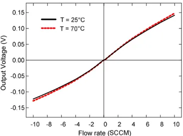
The effectiveness of the proposed method has been also proven by means of the experimental set-up schematically shown in Fig. 1.25. The chip was glued to ceramic DIP cases by means of epoxy resin and wedge bonding was used to connect selected chip pads to the case pins. A PMMA package was designed in order to connect the sensor to a reference gas line, equipped with a precision flow controller (MKS 1179B) with a 10 sccm full scale range. The package was glued to the chip following the procedure described in section 1.3.2. The packaged device was placed inside a hollow aluminium cylinder whose temperature was varied using a Peltier cell driven by an electronic temperature controller. The gas reaches the sensor after passing through pipes drilled through the cylinder walls, in order to get isothermal with the latter. The read out electronics has been developed on two printed circuit boards (PCBs). The first one, connected to a PC via USB, includes a MicroConverter® ADuC842 (Analog Devices) with two 12-bit voltage output DACs used to drive the device heaters. The two DACs have been calibrated to obtain an accuracy of ± 1 mV. The second one, connected to a digital multimeter (HP 3478 A), includes a low noise instrumentation amplifier (AD 620) in cascade with a second order 10 Hz low pass filter used to read the sensor output signal. An application in the National Instruments LabWindows™/CVI environment has been developed in order to drive both the ADuC842 and the multimeter. The offset of the readout electronics was cancelled by subtracting the output voltage measured with both the heaters turned off.
An intrinsic offset of about 24.7 µV has been found when the heaters are biased with the same power (P1 = P2). The applied power unbalance reduced the offset to a residual value of −1.2 µV applying a power ratio P1/P2 of 1.02. The sensor response as a function of the gas flow for two different temperatures, namely 25 °C and 70 °C, is shown in Fig. 1.26. The value of the measured offset at the two temperatures is reported in table 1.III. For comparison, the offset values obtained
Fig. 1.25 – Schematic view of the experimental set-up used for offset and offset thermal drift characterization: DUT indicates the device under test.
with the two heaters biased at the same voltage are also shown. It is important to observe that both the offset and its temperature drift are reduced by almost one order of magnitude. O u tp u t V o lt a g e ( V )
Fig. 1.26 – Amplified output voltage as a function of nitrogen flow rates measured at two different temperatures with offset compensation.
T = 25 °C T = 70 °C Offset with P1/P2 = 1.02 229 µV 385 µV Offset with P1 = P2 (no correction) 2550 µV 3250 µV
Table 1.III – Experimental offset variation (amplified by 150) with temperature.
1.3.5. Heat losses through suspending arms
BDC3s sensors were designed using aluminium as interconnection layer to the heater elements. Aluminium, i.e. a metal layer, was chosen due to the very the low value of sheet resistance, making the voltage drop along the interconnecting pattern negligible with respect to the voltage drop across the heater itself. As an important consequence the power generated by heaters is well determined once their resistance value and the applied voltage or current are known.
Unfortunately, aluminium has also high thermal conductivity, which is responsible of important heat losses along the suspending arms (see eq. (1.7)). Heater temperature is an important parameter for the overall sensitivity of the sensor, as the latter is linearly dependent (in a first order approximation) to the former: the lower is the temperature reached by the heater, the lower the temperature differences between the hot and cold junctions, actually lowering the Seebeck voltages. Minimizing heat losses through suspending arms would reflect on heaters efficiency, enabling the possibility to reach the same overheating with less consumed power. This issue has been addressed in the new design of flow meter in the BCD6s process, by exploiting siliciced polysilicon as interconnecting material instead of aluminium, in fact: (i) it still presents a good electrical conductivity, (ii) it
has lower thermal conductivity as the siliciding process affects only the very surface of polysilicon affecting only few atomic layers, while heat flow concerns the whole section of the polysilicon layer. Figure 1.27 shows the simulated sensor characteristics for positive flow rates in the two cases: aluminium and polysilicon interconnections. In both cases the thermal conductance losses through suspending arms have been introduced in the model following the eqs. (1.7-8), and the same power (4 mW) has been fed to the heater. As expected the structure with polysilicon interconnections has a greater sensitivity. Estimations return a power saving of 40 % when the same sensitivity of the old structures is required.
1.3.6. Low pressure effects on miniaturized thermal flow-meters
While small size of integrated flow meters represents a clear advantage in terms of pass-band and power consumption with respect to traditional macroscopic sensors, it afflicts sensor sensitivity at pressures low enough to make molecule mean free path comparable with the sensor characteristic dimensions. In some applications, such as propellant control for ionic thrusters on board small satellites and gas delivering in semiconductor processing, accurate flow measurements for gases at low pressure is required and as consequence, use of micron scale flow meters may be partially impaired.
In Fig. 1.27, the experimental response of the sensor to nitrogen flow at four different pressures is shown [25]. Authors found that deviation of the output signal from the value measured at atmospheric pressure is less than 3% for pressures greater than 25 kPa, while for lower pressures the signal begins to reduce significantly.
Fig. 1.27 – Thermopiles temperature difference as a function of the flow rate for the two solutions for the heater interconnections: aluminum and unsilicided polysilicon.