SCIENZE CHIMICHE
Ciclo XXII
Settore/i scientifico-disciplinare/i di afferenza: CHIM 02
“IN SITU REAL-TIME INVESTIGATION OF
ORGANIC ULTRA-THIN-FILM TRANSISTORS:
GROWTH, ELECTRICAL PROPERTIES AND
BIOSENSING APPLICATIONS”
Presentata da:
Dr. Santiago David Quiroga
Coordinatore Dottorato
Relatore
Prof. Giuliano Longoni
Prof. Fabio Biscarini
A la memoria de mi madre y de mi abuela;
a mi padre y mis tías, Ana y María Dolores.
large-area displays, low-cost printable circuits, plastic solar cells and lab-on-a-chip devices. Moreover, their possible field of applications reaches from medicine, biotechnology, process control and environmental monitoring to defense and security requirements. However, a large number of questions regarding the mechanism of device operation remain unanswered. Along the most significant is the charge carrier transport in organic semiconductors, which is not yet well understood. Other example is the correlation between the morphology and the electrical response. Even if it is recognized that growth mode plays a crucial role into the performance of devices, it has not been exhaustively investigated.
The main goal of this thesis was the finding of a correlation between growth modes, electrical properties and morphology in organic thin-film transistors (OTFTs). In order to study the thickness dependence of electrical performance in organic ultra-thin-film transistors, we have designed and developed a home-built experimental setup for performing real-time electrical monitoring and post-growth in situ electrical characterization techniques. We have grown pentacene TFTs under high vacuum conditions, varying systematically the deposition rate at a fixed room temperature. The drain source current IDS and the gate source current IGS were monitored in real-time; while a complete
post-growth in situ electrical characterization was carried out. At the end, an ex situ morphological investigation was performed by using the atomic force microscope (AFM).
In this work, we present the correlation for pentacene TFTs between growth conditions, Debye length and morphology (through the correlation length parameter). We have demonstrated that there is a layered charge carriers distribution, which is strongly dependent of the growth mode (i.e. rate deposition for a fixed temperature), leading to a variation of the conduction channel from 2 to 7 monolayers (MLs). We conciliate earlier reported results that were apparently contradictory. Our results made evident the necessity of reconsidering the concept of Debye length in a layered low-dimensional device. Additionally, we introduce by the first time a breakthrough technique. This technique makes evident the percolation of the first MLs on pentacene TFTs by monitoring the IGS in
real-time, correlating morphological phenomena with the device electrical response.
The present thesis is organized in the following five chapters. Chapter 1 makes an introduction to the organic electronics, illustrating the operation principle of TFTs. Chapter 2 presents the organic growth from theoretical and experimental points of view. The second part of this chapter presents the electrical characterization of OTFTs and the typical performance of pentacene devices is shown. In addition, we introduce a correcting technique for the reconstruction of measurements hampered by leakage current. In chapter 3, we describe in details the design and operation of our innovative home-built experimental setup for performing real-time and in situ electrical measurements. Some preliminary results and the breakthrough technique for correlating morphological and electrical changes are presented. Chapter 4 meets the most important results obtained in real-time and in situ conditions, which correlate growth conditions, electrical properties and morphology of pentacene TFTs. In chapter 5 we describe applicative experiments where the electrical performance of pentacene TFTs has been investigated in ambient conditions, in contact to water or aqueous solutions and, finally, in the detection of DNA concentration as label-free sensor, within the biosensing framework.
Negli ultimi decenni l’organica elettronica ha subito un’importante crescita spinta da diversi risultati alquanto incoraggianti e dalle potenziali nuove applicazioni che possono dare luogo agli innumerevoli materiali organici esistenti, tra cui gli schermi flessibili e di grande superficie, i circuiti stampabili a basso costo, le celle solari plastiche e i dispositivi di tipo “lab-on-a-chip”. Inoltre, i campi di applicazione sono così vasti da comprendere medicina, biotecnologia, processi di automazione e monitoraggio dei parametri ambientali, nonché la difesa e la sicurezza. Tuttavia un considerevole numero di domande deve ancora trovare risposta. Tra queste il meccanismo di operazione, che rimane senza essere completamente compreso e la correlazione tra la morfologia e la risposta elettrica dei dispositivi. Nonostante si sia ampiamente riconosciuto l’importante ruolo che il modo di crescita ha sulla prestazione dei dispositivi, non è stata realizzata un’investigazione esaustiva dell’argomento.
Il principale obbiettivo di questa tesi è quindi quello di trovare una correlazione tra i modi di crescita e le proprietà elettriche in transistor a film sottile (TFTs) di pentacene. Al fine di studiare la dipendenza della prestazione elettrica dei TFTs di pentacene al variare dello spessore, si è proceduto all’ideazione e alla costruzione di una strumentazione sperimentale ad hoc, che permettesse di realizzare misurazioni elettriche in tempo reale e caratterizzazioni in situ alla fine della deposizione. Abbiamo provveduto alla crescita di dispositivi TFTs di pentacene in condizione di alto vuoto, variando metodologicamente la velocità di deposizione a temperatura ambiente prefissata. Durante la crescita, la corrente di drain IDS e la corrente di gate IGS sono state monitorate in tempo reale e al
termine di ogni deposizione si è proceduto alla caratterizzazione elettrica in situ. Alla fine si è investigato sulla morfologia ex situ con l’utilizzo di un microscopio di forza atomica (AFM).
Nel presente lavoro si riporta la correlazione valida per TFTs di pentacene tra le condizioni di crescita, la lunghezza di Debye e la morfologia (quantificata attraverso la lunghezza di correlazione). Abbiamo dimostrato che i portatori di carica vengono distribuiti nei layers a seconda del modo di crestita eseguito dal film (che dipende dalla velocità di deposizione per una data temperatura), il quale porta a una variazione del canale attivo dai 2 ai 7 monolayers (MLs). I nostri risultati hanno conciliato altri riportati in precedenza, che sembravano alquanto contradittori e hanno evidenziato la necessità di rielaborare il concetto di lunghezza di Debye in dispositivi a strati a bassa dimensione. Inoltre, per la prima volta, si presenta un’innovativa tecnica che indica l’avvenimento della percolazione attraverso il monitoraggio elettrico della IGS durante la deposizione del film sottile, correlando i fenomeni
morfologici con quelli elettrici.
Il capitolo 1 di questa tesi ci introduce nel mondo dell’elettronica organica e ci spiega il funzionamento del TFT. Il capitolo 2, ci spiega la crescita dei materiali organici, offrendo prima un fondamento teorico per poi passare alla sperimentazione; dopodiché si esibisce la prestazione elettrica tipica dei dispositivi di pentacene e si presenta la suddetta tecnica correttiva sugli effetti della corrente di fuga. Nel capitolo 3 si presenta la strumentazione costruita ad hoc per il monitoraggio elettrico in tempo reale e in situ; si illustrano inoltre alcuni risultati preliminari, assieme alla suddetta tecnica “breakthrough”. Intanto, nel capitolo 4, si riportano i più rilevanti risultati ottenuti in tempo reale e in
situ, che correlano il modo di crescita, le proprietà elettriche e la morfologia dei TFTs di pentacene.
Infine, il capitolo 5, si concentra nello studio sulla risposta elettrica dei dispositivi TFTs di pentacene in contatto con l’ambiente, con acqua e altre soluzioni acquose e, principalmente, della sua applicazione nella biosensoristica come sensore di concentrazione di DNA.
Voglio ringraziare inanzittutto il Dott. Fabio Biscarini per avermi dato la possibilità di svolgere il mio dottorato di ricerca nel suo laboratorio, per il suo incoraggiamento e per l’appoggio che mi ha offerto in questi tre anni e per avermi dato una mano e una dritta quando ne ho avuto bisogno. Voglio inoltre ringraziarlo per la crescita professionale che mi ha permesso di raggiungere in questo periodo della mia vita.
Voglio ringraziare i miei colleghi del gruppo di organica elettronica: Arian Shehu, Pasquale D’Angelo, Cristiano Albonetti, Francesco Borgatti, Pablo Stoliar, Andreas Straub e Stefano Casalini.
Ringrazio anche il resto dei colleghi del laboratorio: Francesco Valle, Eva Bystrenova, Beatrice Chelli, Paolo Greco, Crispin Kegne e Michele Bianchi che, giorno a giorno, si sono resi sempre disponibili ad aiutarmi e ad offrirmi la loro conoscenza. Ringrazio anche chi oggi non lavora più con me, ma che ha saputo lasciarmi una parte di sé: Adina Lazar e Matei Iacobini. Ringrazio specialmente Arian con cui ho lavorato, affrontando le diverse sfide che abbiamo dovuto superare in questo lungo percorso: grazie a te, non solo per l’appoggio professionale ma, suprattutto, per quello umano. Grazie perché molti di voi siete diventati non solo bravi colleghi, ma anche veri amici.
Ultimo, ma non meno importante il mio ringraziamento va ai pilastri della mia vita che sono i miei affetti, la mia famiglia, Paolo e miei amici di sempre: Ariel, Juanjo, Nolwenn, Fer Raballo, Fer Juárez, Meli, Miguel, Amalia, Sara, Talo e gli amici che l’Italia mi ha regalato in “casa Salvini” e che mi hanno sostenuto sempre.
Infine ringrazio chi non ho menzionato ma che, in un modo o in un altro, abbia contribuito ad arricchire la mia vita, permettendomi oggi di essere arrivato fino qui.
Santiago.
Key-Words
Organic Thin Film Transistors Pentacene
Electrical Characterization Real-Time Technique
1
“Introduction to Organic Ultra-Thin-Film Transistors”
1.1 Organic Electronics: A Brief Review ………. 13
1.2 Organic Semiconductors ………. 14
1.3 Charge Carriers Transport in Organic Semiconductors ……….. 16
1.3.1 Charge Carriers in Organic Semiconductors: n-type and p-type ………... 16
1.4 Organic Semiconductor Materials for Organic Thin-Film Transistors ……….. 16
1.5 Operation Principle of Organic Thin-Film Transistors ……….. 18
References ………... 20
2
“Fabrication and Electrical Characterization of Ultra-Thin-Film Transistors”
2.1 Introduction to Organic Growth Dynamics ……… 212.2 Growth Parameters ………. 23
2.3 Experimental Setup for High Vacuum Sublimation ………... 24
2.4 Electrical Characterization ………... 25
2.4.1 Experimental Setup for Electrical Characterization ………... 25
2.4.2 Organic Thin-Film Transistor Parameters ……….. 27
2.5 Experimental Results ………... 29
2.5.1 Electrical Performance of Typical Pentacene TFTs ………... 30
2.5.2 Channel Length Effects on the Electrical Response ………... 31
2.6 Gate Leakage Effects: A Correcting Technique ……….. 32
2.7 Conclusions ……….. 34
References ……… 34
3
“Real-Time and In Situ Electrical Monitoring of Ultra-Thin-Film Transistors:
Experimental Setup and Techniques”
3.1 Introduction ……….. 373.2 Samples Architecture ………... 38
3.3 Sample Cleaning Treatment ………. 39
3.4 Experimental Setup: The Real-Time and In Situ Growth System ………... 40
3.4.1 High Vacuum Chamber and Sample-Holder ……….. 40
3.4.2 Electrical Connections and Software ……….. 43
3.4.3 High Vacuum Connections ………. 45
3.5 Experimental Techniques and Results ………. 45
3.5.1 Electrical Characterization ………. 46
3.5.2 Morphological Characterization ………. 50
3.6 Conclusions ……….. 51
References ……… 51
4
“Correlation Between Growth Mode, Electrical Properties and
Morphological Parameters”
4.1 Introduction ……….. 53
4.2 Experimental Details ……… 53
4.3 Results and Discussion ……… 54
4.4 Conclusions ……….. 58
4.5 Supplementary Information ………. 59
References ……… 61
5
“Biosensing Applications”
5.1 Introduction to (Bio-)Field-Effect-Based Sensor Devices ………... 635.2 Principle of (Bio-)Organic Thin-Film Devices ……… 64
5.3 Environmental Stability of Organic Semiconductors ……….. 64
5.3.1 Electrical Response of Pentacene TFTs in Ambient Conditions ……… 64
5.3.2 Electrical Response of Pentacene TFTs Under Water ……… 66
5.4 Biosensors: Pentacene TFTs for the Recognition of DNA Concentration ……….. 69
5.4.1 Experimental ………... 69
5.4.2 Results and Discussion ………... 70
5.5 Conclusions ……….. 73
References ……… 73
AFM = Atomic Force Microscope
D = Drain
DNA = Deoxyribonucleic Acid
FED = Field-Effect-sensor Device
FET = Field-Effect Transistor
G = Gate
HF = Hydrofluoric Acid
HMDS = 1,1,1,3,3,3 hexamethyldisilazane
HV = High Vacuum
L = channel Length
ML = Monolayer
OTFT = Organic Thin-Film Transistor
S = Source
SAM = Self-Assembled Monolayer
UHQ water = Ultra-High Quality water
UHV = Ultra-High V
acuumV
TH= Threshold Voltage
W = channel Width
= Deposition rate
= Film Thickness/Coverage
= Charge Carrier Mobility
= Correlation Length
In this chapter we briefly review the history of the organic electronics, from the first studies on organic semiconductors, the state-of-the-art until the most recent progress which gives the perspectives for future investigations. We mainly focus on the physical-chemical properties of the organic semiconductors and the role they play on the device performance. In addition, the operation principle of organic thin-film transistors is explained.
1.1 ORGANIC ELECTRONICS: A BRIEF REVIEW
The first studies of electronic properties on organic crystals date back to the early 20th century
[1,2]. In the 1960s, with the discovery of electroluminescence [3,4], the investigation were increased and the basic models for interpreting the charge carrier transport were established [5,6]. It was not until the 1970s that the first application of organic semiconductor started, when the conjugated polymers were successfully synthesized and their doping was controlled [7]. In 1982 the metal-oxide-semiconductor structure was demonstrated, using polyacetylene as metal-oxide-semiconductor and polysilocane as dielectric [8]. Even if the device has not exhibited a great performance, it was recognized as a promising technology.
The milestone of organic electronics technology was the demonstration in 1986 of the first organic field-effect transistor (OFET) or alternatively named organic thin-film transistor (OTFT) [9]. At the same time, the development of organic heterojunction solar cell [10] and organic light emitting diode [11] were reported. Later on, soluble forms of organic semiconductors were developed, opening the possibilities to printable circuits [12,13].
Organic electronics technology exhibit comparable performance to amorphous silicon technology but still remains some order of magnitude lower the performance offered by crystalline silicon devices. For this reason organic electronics technology is not suitable for high-performance applications where high switching capability is of primary importance. On the other hand, organic electronics offers the possibility to deposit a variety of organic materials on a wide range of substrates, from glass and plastic to paper, by using non-conventional processing techniques, such as inkjet printing and roll-to-roll manufacturing [14-17]. This alternative technology can be used in a large number of applications, including flat panel displays [16], organic LEDs [18], photovoltaic cells [19], radio frequency identification tags [20], large-area electronics [21] and sensors [22].
Before a complete industrialization of this alternative technology becomes a reality, several aspects of the device reliability need to be solved (i.e. environmental stability, lifetime, etc). Device reliability lies on a good understand of the electrical properties. Nowadays, the charge carrier transport in organic semiconductors and the injection phenomenon in the organic/Au and organic/oxideinterface are not well understood. The injection controls the physics of the device, not only at the molecular level but also microscopically. The comprehension of this interaction is fundamental to reach a good control of the device characteristics.
We have addressed our studies to the physics of the ultra-thin film transistors, focusing on the charge carrier transport and the variation of the electrical parameters when the device is exposed to different environmental conditions (ambient, water and aqueous solutions).
1.2 ORGANIC SEMICONDUCTORS
The organic semiconductors can be divided in two main classes: i) Low molecular weight materials.
ii) Polymers.
Carbon atoms (C-atom) in organic semiconductors form sp2-hybridization (figure 1.1), where
there are three sp2-orbitals on the same plane (each with one electron) and there is a p
z-orbital
perpendicular to this plane (with the fourth electron).
Figure 1.1 Scheme of the C atom exhibiting the sp2 hybridization geometry. The arrow around the atom
indicates the plane on which the sp2 orbitals lie. Three electrons are distributed on the plane in the orbital sp2,
while the other electron is localized in the pz orbital, perpendicular to the sp2 plane [23].
In an organic semiconductor in which neighboring C-atoms present sp2-hybridization, the overlap
of sp2-sp2 orbitals forms a covalent strong -bond (figure 1.2 a), whereas the overlap of two pz
-orbitals forms a -bond (figure 1.2 b). The whole molecule has both bonds (figure 1.2 c). By comparing, the bonds, which form the backbone of the molecules, are much stronger than the -bonds. The -bonds are a weaker type of bonding due to the distance between the bonding ( ) and the antibonding ( *), thus the energy levels is lower [24]. On an isolated molecule, the energy levels are
discrete and known as molecular orbitals. The two most interesting molecular orbitals are the highest occupied molecular orbital (HOMO) and the lowest unoccupied molecular orbital (LUMO). The energy gap is the difference of energy between them (figure 1.2d).
Molecules, in which neighbouring carbon atoms are sp2 hybridized, forming delocalized clouds
of -electrons, are termed -conjugated. Both low molecular weight and polymers are conjugated materials. There is some ambiguity in the exact configuration of the bonding structure and the real molecule is a superposition of all these representations. Figure 1.3 shows two resonance structures of the polyacetylene.
The - *-transition for conjugated materials has an energy gap which usually varies in the range 1.5-3 eV. For the family of the polyacenes, shown in figure 1.4, the energy gap can be modified depending on the degree of conjugation in a molecule. The larger the conjugated network is on a molecule, the smaller the HOMO-LUMO gap will be, because for longer chains the separation between energy levels is smaller.
One important different between low molecular weight materials and polymers is the possibility of processing for obtaining thin-films. Small molecules can be deposited by sublimation, while the polymers can only be processed from solution by spin-coating or printing techniques. A number of low-molecular materials can also be grown as single crystal, which allows us to investigate the intrinsic properties [23].
Figure 1.2 Ethylene molecule representations: (a) top view, showing the sp2 orbitals of C-atom (the pz
orbitals are perpendicular to the page), and the s orbitals of the H-atom; (b) -bonds formed by the overlapping of sp2 orbitals and -bonds formed by the overlapping of pz orbitals; and (c) the whole hybridization; (d) the
energy level.
Figure 1.3 Two resonance structures of the polyacetylene [23].
Figure 1.4 Molecular structure of the first five polyacenes and their predicted and measured HOMO-LUMO transitions [25]. Note that the C-atom positions for pentacene have been tagged. Positions 6,13 on pentacene have been identified as the most exposed to oxidation.
Energy Gap
(c)
1.3 CHARGE CARRIER TRANSPORT IN ORGANIC SEMICONDUCTORS
The presence of extended -conjugated electrons makes possible to design a large variety of both kinds of organic semiconductors, low molecular weight materials and polymers. Stable molecules with large, polarisable -systems interact via dispersive forces typically Van deer Waals forces [26] which are weaker than the covalent bonds in inorganic semiconductors like Si. The organic materials present a weaker interaction between molecules which allows the transfer of charge carrier from molecule to molecule. This charge can be moved on along the molecule by applying an electric field, generating charge states on organic semiconductors. Translated in a band-like picture, this implies a narrower -band. In terms of charge mobility, it is possible to reach values between 1 and 10 cm2/Vs
in the most perfect molecular crystals. In contrast, in inorganic crystalline semiconductors, charge carriers move as highly delocalized plane waves in wide energy bands with a very high mobility (~ 103 cm2/Vs). In this case, the mobility is limited by lattice vibrations (phonons) that scatter the carriers
and thus it is reduced as the temperature increases.
In the case of organic thin films, which are technologically relevant, the scenario is even more complex than in single crystals. Thin-films have the great advantage to be fabricated at low cost with non conventional techniques. On the other hand, thin-films exhibit lower performance with respect to single crystals. Highly ordered thermally sublimed oligomers often give rise to polycrystalline films and solution processed polymers often yield highly disordered or amorphous films. Band transport is not applicable in this case, due to the presence of structural disorder, large number of defects and grain boundaries that are intrinsic of thin films. Charge carriers are transported by thermally assisted hopping between localized states and are scattered at every step. Hopping is assisted by phonons and the mobility generally increases with temperature. In this case, charge carrier mobility is strictly connected to the ordering range of the thin-film [26, 27], and it is crucial to find optimized conditions for the thin-film deposition for improving the long-range ordering and for minimizing defects in the film structure. Even though there has been a lot of effort in the last twenty years on this argument, many basic aspects related to the physics of organic semiconductor thin-films remains unclear.
1.3.1 CHARGE CARRIERS IN ORGANIC SEMICONDUCTORS: n-type and p-type
The transport of charge in organic semiconductors typically follows a hopping mechanism and is governed by the class of transport models related to highly disordered systems. The density of states of these disordered systems is often asymmetrical and presents a significantly larger barrier to the formation of one or another type of carrier. Many amorphous or polycrystalline organic semiconductors sustain either positive or negative charge carriers, but not both.
In conventional, inorganic semiconductor technologies, n-type and p-type refer to the type of dopant, and therefore majority carrier present in a semiconductor. In crystalline materials both holes and electrons can usually be transported reasonably well. Disordered electronic systems, on the other hand, often only support or strongly favor one type of charge carrier and are more properly referred to as hole or electron transporting. It is, nevertheless, common in the literature to refer to hole transporting disordered semiconductor materials as p-type and electron transporting materials as n-type because this describes their majority carriers and semiconducting behavior. An important complication of both p-type and n-type semiconductors is their poor stability against oxidation and reduction reactions.
1.4 ORGANIC SEMICONDUCTOR MATERIALS FOR ORGANIC THIN-FILM-TRANSISTORS
As mentioned above, organic semiconductors are divided in two big groups, polymers and low weight materials (namely also small molecules). How these elements are connected has a deep influence on how they are processed and on how they perform. Along the small molecules, pentacene
modified by reacting organic semiconductor with strongly electropositive or electronegative materials such as alkali metals (e.g. K) [28] and metals (e.g. I) [29].
The number of small molecules is practically infinite. Usually, small molecules can be deposited through thermal sublimation processes, but several of them have been functionalized to be soluble and can be deposited from solution. The family of acenes and their derivatives shown in figure 1.4, has fused rings, which are planar and rigid, leading to superior stacking properties. Many of these materials form polycrystalline films when they are deposited at room temperature. This superior order allows a better - overlap between the neighboring molecules, improving the overall device performance. This better performance is made evident through the charge mobility measurement. Pentacene forms polycrystalline films on insulating substrates (like SiO2), exhibiting good transport
properties. Under appropriated conditions, pentacene and can also form large single crystals [30].
Figure 1.6 Evolution in the OTFTs performance, in term of charge mobility, for different materials [24,26]. The p-types semiconductors are inside the box. The deposition technique used in each case is indicated in brackets as: (V) vacuum evaporated, (sc) single-crystal, (S) solution processed. The amorphous hydrogenated silicon (a-Si:H) mobility is shown as a reference (gray strip).
Pentacene is relatively easy oxidized especially at the 6,13 positions, which disrupt transport and crystallization on devices (see tagged positions in figure 1.4). This often leads to polymorphic crystal growth, which can lead to mismatched grains, thus a reduction of the performance. One alternative to overcome this problem is to synthetically attach bulky groups to the 6,13 positions of pentacene. When the groups are properly selected this passivates the most reactive sites on the pentacene molecule and constrain the crystallization into a single highly favorable phase [31].
Figure 1.6 shows the evolution of OTFTs performance, in term of mobility, for several different p-type and n-type organic semiconductors. The mobility is plotted in logarithmic scale while the time axis (in year) is plotted in linear scale. It can be seen that mostly of these organic semiconductors presents charge mobility higher than this one exhibited by the amorphous silicon. The performance
depends not only on the material but also on the deposition technique used and the kind of device (p-type or n-(p-type).
Nowadays, the charge mobility requirements are mostly satisfied but before their industrialization will be a reality, it is necessary to assure reliability of OTFTs performance under environmental and working conditions. In this thesis, we will present some experiments in ambient conditions and in contact to water and other aqueous solutions in chapter 5.
1.5 OPERATION PRINCIPLE OF ORGANIC THIN-FILM TRANSISTORS
Until now, we have made an introduction to the organic materials, the development of organic semiconductors, focusing on their properties. Moreover, we have shown the evolution of the OTFTs performance and we introduced the pentacene, which is used in all our experiments presented in this work. In this section we present the OTFT, including device architecture, operation principle and modeling of the electrical behavior.
A three-dimensional schematic view of an organic thin-film transistor is shown in figure 1.7. It is a planar device formed by a gate made of doped-Si (n-type doped Si when the organic material is pentacene); a dielectric, which is generally made of SiO2; source and drain contacts made of Au; and
the organic semiconductor (in our experiments, pentacene). L is the channel length, the distance between the source and the drain contacts. W is the channel width, the transverse distance of the Au structure. Source and drain are isolated from the gate through the dielectric, thus forming a metal-insulator-semiconductor (MIS) structure. Usually, the Au structure in the channel presents an interdigitated form, which it is useful for saving space on the substrate (especially for big W).
Figure 1.7 Schematic 3D view of an organic thin-film transistor. In our experiments the organic semiconductor is pentacene and the dielectric is thermally grown SiO2.
The OTFT is a field-effect device in which the gate voltage VG modulates the charge flow between source and drain electrodes. In particular, VG induces free charge carriers on the organic
semiconductor, whereas the drain-source voltage VDS, drives these charges from the source contact S
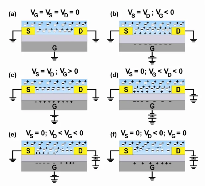
to the drain contact D. The operation principle for a p-type OTFT is illustrated in figure 1.8. Initially, the OTFT is not connected to any voltage and the structure is comparable to the capacitor (figure 1.8a). When a negative gate voltage is applied, a hole accumulation layer is formed in the semiconductor adjacent to the dielectric (figure 1.8b). In contrast, if a positive VG is applied, then a
depletion region is formed (figure 1.8c). The accumulated holes can flow from source to drain if a small voltage between these two contacts is applied (figure 1.8d). Under these conditions the OTFT operates in linear regime. As the drain voltage becomes more negative VD ≤ VG, a depletion zone will
be formed at the drain side and the channel will be pinched off (figure 1.8 e-f). This condition corresponds to the saturation regime.
Figure 1.8 (a) Schematic of operation of an organic thin-film transistor, using p-type organic
semiconductor: + indicates a positive charges (holes) in the semiconductor, whereas (-) indicates the negative fixed charge. (b) Creation of a hole accumulation layer when a negative gate voltage VG is applied. (c)
Depletion of holes from the semiconductor, which is indicated by the dotted line, when a positive VG is applied.
(d) Charge flow in the channel due to a difference of voltage applied between source and drain. (e) Creation of a
depletion zone by the drain contact when the drain voltage is more negative than the gate voltage. (f) The channel is completely depleted from holes because the VG becomes more positive [32].
In a first approximation, the current-voltage characteristics, in linear and saturation regime, can be modeled through the equations valid also for crystalline silicon FETs [24]:
for: (VGS - VTH)< VDS (1.1)
for: (VGS - VTH) ≥ VDS (1.2)
where Cox is the capacitance of the dielectric per unit area (F/m2), is the charge carrier mobility and
VTH is the threshold voltage. Both electrical parameters and VTH will be explained better in the next
REFERENCES
[1] J. Koenigsberger, K. Schilling, Ann. Physik 32, 179 (1910). [2] M. Volmer, Ann Physik 40, 775 (1913).
[3] M. Pope, H. Kallmann, and P. Magnante, J. Chem. Phys. 38, 2042 (1963). [4] W. Helfrich and W.G. Schneider, Phys. Rev. Lett. 14, 229 (1964).
[5] E. A. Silinsh, Organic molecular crystals. Springer, Berlin 1980.
[6] M. Pope and C. E. Swenberg, Electronic processes in organic crystals, Clarendon Press, Oxford 1982.
[7] C. K. Chiang et al., Phys. Rev. Lett. 39, 1098 (1977).
[8] F. Ebisawa, T. Kurokawa, and S. Nara, J. Appl. Phys. 54, 3255 (1983). [9] A. Tsumura, H. Koezuka, T. Ando, Appl. Phys. Lett. 49, 1210 (1986). [10] C. W. Tang, Appl. Phys. Lett. 48, 183 (1986).
[11] C. W. Tang and S. A. VanSlyke, Appl. Phys. Lett. 51, 913 (1987).
[12] K. Y. Jen, G. G. Miller, and R. L. Elsenbaumer, J. Chem. Soc.-Chem. Commun. 17, 1346 (1986). [13] A. Assadi et al., Appl. Phys. Lett. 53, 195 (1988).
[14] G. H. Gelinck, T. C. T. Geuns, D. M. de Leeuw, Appl. Phys. Lett. 77, 1487 (2000). [15] S. R. Forrest, Nature 428, 911 (2004).
[16] G. H. Gelinck et al., Nature Mater. 3, 106 (2004). [17] M. Halik et al., Nature 431, 963 (2004).
[18] J. H. Burroughes et al., Nature 347, 539 (1990) [19] G. Yu et al., Science 270, 1789 (1995)
[20] E. Cantatore et al., Int. Solid State Circuits Conf. 15.2, 2006. [21] W. Clemens et al., J. Mater. Res. 19, 1963 (2004).
[22] L. Wang et al., Anal. Bioanal. Chem. 384, 310 (2006).
[23] Ioannis Kymissis, Organic Field Effect Transistors: Theory, Fabrication and Characterization, Springer, New York, 2009.
[24] Z. Bao, J. Locklin, Organic Field-Effect Transistors, CRC Press, Boca Raton, 2007. [25] C. W. Scherr, J. Chem. Phys. 21, 1582 (1953).
[26] C. D. Dimitrakopoulos, P. R. L. Malenfant, Adv. Mater. 14, 99 (2002).
[27] W. Brütting, Physics of organic semiconductors, WILEY-VCH, Weinheim (Germany), 2005. [28] T. Minakata, M. Ozaki, H. Imai, J. Appl. Phys. 74, 1079 (1993).
[29] Y. Matsuo, S. Sasaki, S. Ikehata, Phys. Lett. A 321, 62 (2004).
[30] F.-J. Meyer zu Heringdorf, M. C. Reuter, R. M. Tromp, Nature 412, 517 (2001).
Here the fabrication of organic ultra-thin-film transistors by organic molecular beam deposition is described. We present a home-made experimental setup for performing electrical characterization of electronic devices under controlled atmosphere. The extraction of the main device parameters is detailed. Finally, the electrical characterization of pentacene devices is discussed and a technique for correcting disturbing effects produced by the leakage current is introduced.
2.1 INTRODUCTION TO ORGANIC GROWTH DYNAMICS
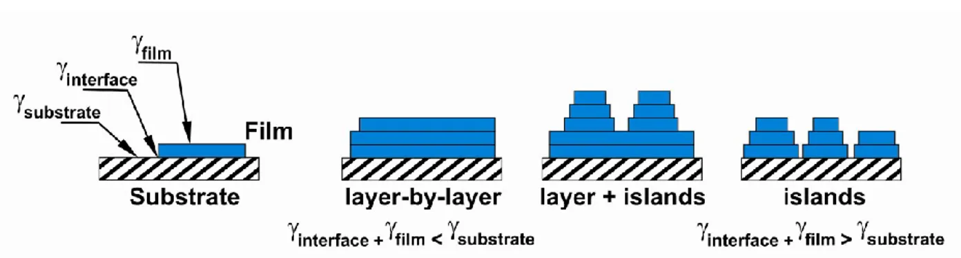
We focus on organic thin-film transistors (OTFTs) grown by organic molecular beam deposition (OMBD) technique. The growth of organic molecule films is a non-equilibrium phenomenon, where the growth kinetics plays a crucial role. The organic thin-film growth is complex and this section presents only a brief description of some features related to our experiments. Figure 2.1 shows different kinetic processes relevant for the growth by OMBD, such us nucleation, surface diffusion, and desorption [1]. Classically growth phenomena are classified according to three growth modes (figure 2.2):
i) Frank-van-der-Merwe or layer-by-layer.
ii) Stranski-Krastanov (layer-by-layer and, above a critical thickness, island growth).
iii) Vollmer-Weber or island growth (from the first monolayer). This can also occur following nucleation of crystalline nuclei with no preferred
crystallographic orientation on the basal plane.
The growth modes can be described using different arguments, such as epitaxy and the surface and interface energies. The epitaxy refers to systems where there is a commensurate relationship between the molecular positions in the growing layer and the substrate. Epitaxy often is accompanied by a lattice mismatch between the film and the substrate, which is not only important from the crystallographic point of view, but also influences the growth beyond the first monolayers [2]. This suggests that by a proper selection of the substrate the crystal structure of the epitaxial layers can be controlled from the first ML (adjacent to the substrate) to higher layers [3]. In the case of molecular semiconductors, this concept is useful to understand the organization of the molecules at the metal-semiconductor interface in devices, although the metal films are polycrystalline. In the channel, usual dielectric surfaces (e.g. silicon oxide) are amorphous and the concept does not apply.
Another approach to describe the various relevant interactions uses the concept of surface and interface energies. The relevant surface energies are: the free substrate surface, s, the film surface, f ,
and the film-substrate interface, i. Depending on these energies, the thin-film growth follows one of
the three growth modes described above. Surface energy plays an important role in the growth of organic semiconductors both on the metal electrodes and on the dielectric channel. Several works have reported the use of different methodologies for changing the substrate surface energy, thus
modifying the growth mode. One of the most common approaches is the use of self-assembled monolayers (SAMs) [4-6].
Figure 2.1 Schematic of dynamic processes relevant in the thin-film growth by organic molecular beam deposition technique [7].
There are some other considerations concerning the organic growth exclusively:
i) The internal degrees of freedom: molecules should be considered as objects with orientational and vibrational degrees of freedom. The orientational degrees of freedom are related to changes of the molecular orientation during the growth (lying-down and standing-up). The vibrational degrees of freedom affect the interaction with the surface as well as the thermalization and the diffusivity [8].
ii) The Van-der-Waals interactions are more important, thus implying that relevant temperature scales for sublimation, diffusion, annealing are lower. It is important to mention that for reactive surfaces the diffusion is limited and then the reorganization of the film is hampered. In the extreme case of very reactive surfaces, the molecules can dissociate upon adsorption [9,10]. iii) In addition to the sources of disorder known from inorganic system (i.e.
vacancies), organics frequently crystallize in low-symmetry structures, which can lead to multiple domains, which further increases the disorder o [8].
Figure 2.2 Growth modes of organic thin-films grown by OMBD, from the point of view of the surface and interface energies: layer-by-layer, layer plus island and island growth.
2.2 GROWTH PARAMETERS
Pentacene is the most studied organic semiconductor, owing to its excellent properties as active layer in OTFTs [11]. Morphological scaling analysis on sub-ML thin-films have shown that the smallest stable nucleus is composed of four molecules [12]. Single crystalline island size can reach 0.1 mm [13]. Pentacene films show two different polymorphic structures: Campbell’s or “bulk” phase [14] and the so-called “thin film” or Holmes phase [15]. Recently, a controversial third pentacene polymorph present in thin-films with enhanced physical properties has been reported by Siegrist et al.[16]. For thicker films, the Holmes and Campbell phases coexist depending on the growth conditions [17]. The bulk crystalline structure is shown in figure 2.3.
We focus on the study of pentacene thin-film growth on SiO2. In order to achieve a high
performance of pentacene devices, it is crucial to have a control of the morphology, [18,19] optimizing the thin-film organization, and minimizing the structural defects [20]. The growth mode and the film morphology are strongly dependent on the following parameters:
i) Deposition rate [2 23 .
ii) Substrate temperature Tsubstrate [23].
iii) The surface energy [24].
iv) The kinetic energy of the incident molecules [25].
Verlaak et al. [24], have studied the thermodynamics of nucleation for pentacene on technologically-relevant substrates such as SiO2 with and without different primers, as a function of
Tsubstrate and . The nucleation phase diagram is shown in figure 2.4(a). By inspection of the phase
diagram, it can be noted that only films grown below the dotted line (2D nucleation) can grow in a layer-by-layer mode. Since growth mode depends also on the surface energy and roughness, there can be a transition to 3D growth, with enhanced stacking of monolayer terraces before the completion of the underlying layers as the film grow. This is frequently observed in the case of pentacene, and the phenomenology can be ascribed to the spatial dependence of the van der Waals interaction between the condensing molecules and the growing islands with increasing thickness. In fact, many layers are needed to reach a saturation in the spatial dependence of the interaction. This affects on one hand the surface energy, and hence the nucleation rate and nuclei dimensionality. On the other hand, it also affects the self-diffusional barriers including the Schwoebel barrier. The latter is the energy barrier for molecules to diffuse across a terrace edge, which would lead to smoothening of the stacked structures and the completion of the underlying layers. The increase of the Schwoebel barrier vs thickness leads to enhance the effective upward flow of molecules which accounts for the 3D stacking. Ruiz et al. have developed a kinetic model based on Master equation to predict the evolution of pentacene films [26]. The parameters of the model are the diffusional rates across the pentacene surface, and time is renormalized to the inverse deposition rate. The evolution of the occupancy, which is the coverage of each monolayer, is shown in figure 2.4(b). The model can be parameterized by fitting X-ray scattering [27] or AFM roughness dynamic scaling data [28]. The outcome of the model is that at the early stages growth occurs layer-by-layer, viz. no upper layer starts growing before the completion of the
underlying monolayer. Above 1-2 monolayers, the stacking of incomplete layers starts and get enhanced as thickness grows. For instance the growth of the fourth monolayer starts at the completion of the second ML and finishes after 5 MLs have been deposited. The fifth monolayer appears at 2.5 ML nominal thickness and is completed beyond 6 ML. This is in agreement with the roughness scaling vs thickness reported in ref. [29, 30].
Figure 2.3 (a-b) Bulk (Campbell’s) crystalline structure of pentacene [14]
Figure 2.4 (a) Growth modes for pentacene assuming ψmol-sub = 0 (interaction strength between one
molecule and the substrate is zero) [24]. Below the solid line, three-dimensional (3D) nucleation is possible. For growth conditions below the dashed line, two-dimensional (2D) nucleation is possible. 2D nucleation becomes more likely than 3D nucleation only below the dotted line. In a first approximation, only growth conditions below the dotted lines will give rise to continuous films. (b) Evolution of the coverage as a function of the film thickness for pentacene on SiO2 [26].
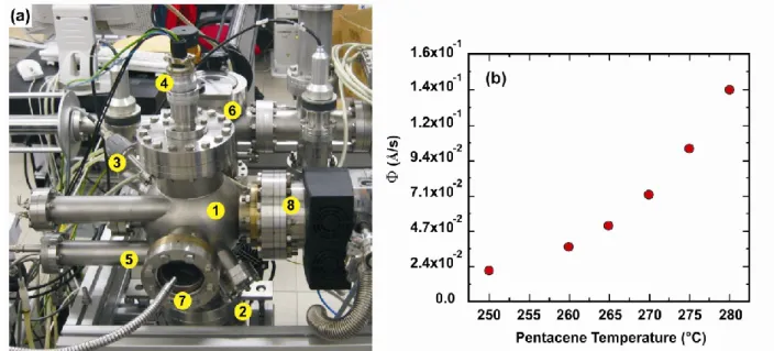
2.3 EXPERIMENTAL SETUP FOR HIGH-VACUUM SUBLIMATION
The organic growth of molecules like pentacene or sexithienyl is performed by sublimation in an experimental setup composed of: high vacuum (HV) chamber, Knudsen cell, quartz crystal microbalance, shutter and sample-holder. In this chapter we describe the main experimental setup used in our group (figure 2.5a). In chapter 3 we present a more complex experimental setup, built during this thesis, which allows us to carry out a series of characterization experiments in real-time and in situ conditions.
thermocouple mounted on the sample-holder and can be also increased by using a second PID.
For our experiment we use pentacene (Fluka-N° 45797). Purification of organic materials is essential for assuring that the grown thin-film is reasonably free of impurities which may act as traps or dopants in an electronic device [10]. There are several techniques for purification. The simplest technique is the outgassing, which is what we used. Another popular technique is the gradient sublimation, which is more sophisticated [31]. Outgassing consists of heating the organic material close to the sublimation point in HV for a few hours. This allows removal the traces of solvent and smaller oligomers or lighter precursors. The absence of H2O and O2 in HV minimize thermal
degradation of the material. Once outgassed, pentacene is kept under HV. Growth in a HV environment assures that a minimal density of impurities and defects will be incorporated into the film. The degree of impurities which may be deposited on the substrate depends on the quality of the vacuum and the deposition rate, as slower rates occur in longer time [10].
Figure 2.5 (a) HV sublimation chamber. The main elements are: (1) HV chamber; (2) Knudsen cell; (3)
quartz crystal microbalance; (4) sample-holder manipulator; (5) shutter; (6) fast-entry; (7) viewport + light, for optical monitoring; (8) connections to turbomolecular and scroll pump. (b) Rate of deposition vs pentacene temperature as measured from a calibrated quartz crystal microbalance.
2.4 ELECTRICAL CHARACTERIZATION
The electrical characterization of OTFTs is a fundamental tool for investigating charge transport phenomena in organic materials. OTFTs are quite sensitive to the environmental conditions at which they are exposed. For this reason a special experimental setup for performing electrical characterization under controlled atmosphere was built. In chapter 5 we will present and discuss experiments related with OTFTs applications in the biosensing field in which the devices are exposed to aqueous solutions.
This section dedicated to the electrical characterization of organic ultra thin-film transistors is divided in two parts. In the first part we outline the home-made experimental setup for electrical
characterization and the second part is focused on the techniques for extracting electrical parameters, in which we are interested.
2.4.1 EXPERIMENTAL SETUP FOR ELECTRICAL CHARACTERIZATION
We have designed and mounted a home-built experimental setup to investigate the electrical response of OTFTs in either high vacuum HV or inert gas atmosphere. All parts of this system were entirely designed and assembled at the CNR-ISMN laboratories, and some critical components were manufactured in CNR machine shop. The system is shown in figure 2.6. It consists of a HV chamber (1) with front entry (2); a top viewport for optical monitoring (3) of the inside through a video camera (4); feedthroughs for gases (controlled by leak valves) and the electrical connections.
Figure 2.6 Integral system for electrical measurements under controlled atmosphere. (a) Main view: (1) HV chamber; (2) front entry; (3) viewport; (4) video camera; (5) pumping connection. (b) Top view. The sliding tray (6) is visible inside the HV chamber. (c) Interior view of the HV chamber showing the test pattern (7) and the piezoelectric motors (8). (d) View of a test pattern; the probes (9) which are connected to the piezoelectric motors are approached on the source and drain contacts by means of a video-assisted joystick which moves the piezoelectric motors.
The samples are introduced in the HV chamber from the front entry. The feedthroughs and other electrical connections, vacuum gauges and thermocouples for monitoring the temperature in different points inside the HV chamber, are located at the backside. The pumping system (5) consists of a turbomolecular pump (Varian TV81-M) coupled to a scroll pump. The minimum base pressure obtained with the scroll pump is 1 mbar. With the turbo molecular pump in regime the pressure can go down to 10-4 mbar. Inside the HV chamber there is a sliding tray (6) with a platform on top, which
contains a Peltier element for increasing or decreasing the substrate temperature Tsubstrate in the range
0-150°C. On this platform, an electromechanical system was mounted. This electromechanical system consists of three actuators (8), each carrying an etched W probe (9) connected to a feedthrough. Each actuator is made of three piezoelectric motors (Physik Instrumente, PILine® M-6624V0X), one for
performed. Coaxial cables are used for connecting the probes to the external measurement unit, in order to reduce environmental electrical noise. The measurement unit consists of a general purpose dual channel source/meter unit Keithley 2612, which is remotely controlled by a dedicated software. The electrical connections of the three probes to the measurement unit are schematically shown in figure 2.7.
Figure 2.7 Connection of Keithley 2612 source/meter unit to the integral system for electrical measurements under controlled atmosphere. The gate probe is connected to the HI terminal of channel A, the drain probe is connected to HI terminal of channel B, and the source probe is connected to both LO terminals of channel A and channel B.
2.4.2 ORGANIC THIN-FILM TRANSISTOR PARAMETERS
According to eq. 1.1 and 1.2 the drain source current IDS depends on two independent voltages,
the drain source voltage VDS and the gate source voltage VGS. For this reason, the current-voltage
curves can be plotted in two different ways:
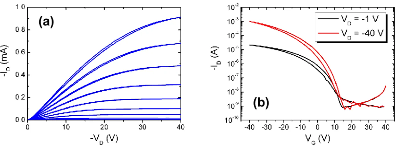
i) Output characteristics (figure 2.8 a). ii) Transfer characteristics (figure 2.8b).
In the first case, a set of drain source current is plotted as a function of drain source voltage for a range of gate source biases; in the second case, the drain source current is plotted as a function of the gate source voltage for a fixed drain source voltage.
From the output curves the regime of operation can be identified, i.e. linear or saturation regime. Then the transfer characteristics are acquired in linear and saturation, in order to extract the following parameters: mobility m, threshold voltage VTH, subthreshold slope, ON/OFF ratio and
Figure 2.8 Electrical characterization of a pentacene thin-film transistor performed by using the integral system for performing electrical measurements under controlled atmosphere. These curves were acquired under vacuum at RT. (a) Output curves. VGS was swept from 10 V (bottom) to -50 V (top) at steps of 5 V. The dashed
line separates the linear from the saturation regime. (b) Transfer characteristic curve at VDS = -1 V (linear
regime). The measurement was performed by applying dual gate sweep (forward/backward). The curves do not exhibit hysteresis.
CHARGE CARRIER MOBILITY
The charge carrier mobility is referred to the majority carriers (holes in our case) in the semiconductor material, and it is expressed in units of cm2/Vs. is usually derived from either
saturation or linear approximations given from equations 1.1 and 1.2. For the linear approximation, a linear fit of the ID vs. VG transfer curve (VD = -1 V) in the region (VG-VT) << VD is performed, and the
mobility is extracted from the slope using equation (1.1). For the saturation approximation, a linear fit of the (ID)1/2 vs. VG transfer curve (VD = - 40 V) in the region (VG-VT) ≥ VD is performed, and the
mobility is extracted from the slope using equation (1.2), as it is shown in figure 2.9.
Figure 2.9 Typical transfer characteristic of a pentacene thin-film transistor. Square-root of the drain source current IDS (in the saturation regime) vs gate source voltage VGS. The intersection between the straight
line and the VGS axis gives the VTH value, while the charge mobility is calculated by applying the slope of the
SUBTHRESHOLD SLOPE, ON/OFF RATIO AND PINCH-OFF VOLTAGE
The subthreshold slope is extracted at the steepest point in the plot of log(IDS) vs VGS (figure
2.10) It is reported in mV/decade, i.e. mV of VGS for every decade of IDS modulation. Smaller values
in these units correspond to a larger slope, which is in general the most desirable.
The ON/OFF ratio is the maximum (on) IDS value divided by the minimum (off) IDS value,
obtained from a transfer (IDS vs. VGS) measurement. This ratio characterizes the ability of the device to
switch the semiconductor channel on and off. We note that the (off) IDS must be greater than the
minimum current the instrument can measure, in order to be determined. Otherwise, the measure will show the internal noise or dark current. Stray capacitances and parasitic effects can also corrupt the measurement. These phenomena can be present in our case, since measured dark current is ~10 pA, pentacene ultra-thin-films in their off region can have very low conductivity. So, the extracted on/off ratio must be considered as the lower limit, and its value at the present can be even greater.
The intersection between the fitted straight line and the VGS axis in figure 2.10 gives the
pinch-off voltage that is the voltage at which the transistor turns on. Like the ON/OFF ratio, the extracted VPinch-Off value depends on the minimum measurable current. Even if this value does not have a
physical definition, VPinch-Off together with the threshold voltage VTH give practical information about
the extension of the subthreshold regime.
Figure 2.10 Typical transfer characteristic of a pentacene thin-film transistor. Drain source current IDS in
log scale vs gate source voltage VGS in linear scale. The subthreshold slope, the pinch-off voltage and the
ON/OFF ratio are shown.
2.5 EXPERIMENTAL RESULTS
Here, we show a series of experiments performed in order to characterize pentacene TFTs by applying the techniques above described. In addition, we present an innovative technique for correcting the disturbing effects produced by the leakage current, which is very useful for extracting the real electrical parameters.
2.5.1 ELECTRICAL PERFORMANCE OF TYPICAL PENTACENE TFTs
A set of 16 devices was fabricated under the same nominal conditions. The devices have a channel length (L) of 20 and 40 m and width (W) of 11200 and 22400 m, respectively. Pentacene was thermally sublimed at room temperature under HV (base pressure 1.10-7 mbar). The deposition
rate used was 2.5 ML/min and the final nominal thickness was 15 nm. Subsequently, all devices were electrically characterized under vacuum ( 10-4 mbar). It is important to mention that all the samples
were treated before deposition, following the same cleaning protocol. Although, the cleaning treatment will be explained in details in chapter 3, we need to remind that the nature of the surface (e.g. roughness and clean conditions) is crucial for obtaining the same growth mode and reproducible electrical performance. Typical output and transfer characteristic curves of pentacene thin-film transistors are shown in figure 2.11(a) and (b), respectively.
Figure 2.11 Typical electrical characteristics of pentacene thin-film transistors with L = 40 m and
W = 22.4 mm. (a) Output curves. The VGS was swept from 10 V (bottom) to -40 V (top) at steps of 5 V.
(b) Transfer characteristic curves in linear (VDS = -1 V) and saturation regime (VDS = -40 V).
A non-ohmic contact response is slightly visible from the output characteristics in figure 2.11(a). Its origin lies in the electronic structure [32], the structural and morphological disorder of the organic/metal interface [6,33]. The hysteresis is due to exposition to ambient conditions before the electrical characterization. In contact to the ambient, the sample can be affected by several elements, such as humidity or oxygen [34,35].
The OTFT parameters above introduced, were extracted for each transfer characteristic curve in linear and saturation regime. The mean value and the standard deviation are shown in Table 2.1. From the table 2.1, we can noticed that the pentacene TFTs show comparable linear and saturation charge mobilities around 0.1-0.2 cm2/V.s, which are close to the highest values reported in literature for
bottom contact pentacene devices on bare SiO2 surface [36]. The mobility is well reproduced from
sample to sample. High ON/OFF ratios are also obtained. The threshold voltages are near zero and pinch-off voltages are positive. Both, threshold voltage and pinch-off voltage show a higher dispersion with respect to mobility, due to sample to sample variations, but this is completely in agreement with literature.
(a)
Std. dev
0.05
3.2
4.4
-
0.63
Saturation regime (V
D= -40 V)
(cm
2/Vs)
V
TH(V)
V
Pinch-Off(V)
I
ON/I
OFFSubthreshold
Slope (V/dec)
Mean
0.18
0.4
18.6
4×10
71.48
Std. dev
0.05
3.4
7.8
-
0.69
Table 2.1 Electrical parameters extracted from 16 pentacene thin-film transistors grown at the same conditions: 15 nm, 2.5 ML/min at room temperature.
2.5.2 CHANNEL LENGTH EFFECTS ON THE ELECTRICAL RESPONSE
The electrical behaviour of the OTFT can substantially differ when the channel length varies. This can be easily observed from the output characteristics shown in figure 2.12. For L = 2.5 m it can be seen that the drain current no longer saturates for high gate voltages. This behaviour may suggest the presence of short channel effects, even though L is much larger than the dielectric thickness (dSiO2 ~ 230 nm).
Figure 2.12 Measured output curves for various channel length (L); the gate voltage was swept in between 10 V and -50 V at steps of 5 V.
The charge carrier mobility and the threshold voltage were investigated as a function of channel length. An analysis of the transfer curves shows a systematic shift of the threshold voltage with the channel length. The threshold voltage shows a 1/L dependence (figure 2.13a). This behaviour is typically observed when short channel effects are manifested. For the same L, comparable values of charge mobility are obtained in both kinds of substrate as shown in figure 2.13(b). The pentacene TFTs were grown under the same conditions, which shows the good reproducibility of our devices.
Figure 2.13 (a) Threshold voltage; and (b) charge mobility measured in linear regime, as a function of the
channel length L.
2.6 GATE LEAKAGE EFFECTS: A CORRECTING TECHNIQUE
Gate Leakage IG ideally is zero, at all bias conditions. Several different factors can lead to gate
leakage, affecting the performance of many circuits. Some of the most important factors are [37]: (i) Inhomogeneities of the dielectric thickness.
(ii) Dielectric stress induced by prolonged exposure time to high electric field. (iii) Mechanical damage of the dielectric layer.
(iv) Poor isolation between the organic layer and the gate. This point is usually resolved by adding a mask on the substrate, which leaves the active channel area free but covering the rest (especially over the edges) during the organic thin-film growth.
Figure 2.14 Schematic of an organic thin-film transistor. Two currents are monitored during the electrical characterization, ID and IG.
where ID, IS and IG are the effective current that flows in the drain, source and gate, respectively.
During the electrical characterization two currents are monitored, drain current ID and gate current IG.
IG = IGS + IGD (2.2) and ID = IDS - IGD (2.3)
The current in which we are interested is the channel current, i.e. drain source current IDS. By
combining equations (2.9):
IDS = ID + IG -IGS (2.4)
If VD = 0, then IDS = 0 and, by considering a symmetrical OTFT architecture, IG is divided in two
identical parts, IGD and IGS. In this case:
IGS(VD = 0) = IG + ID (2.5)
Since VS = 0 in all cases, we assume IGS given by eq. (2.12). If VD ≠ 0, drain source current is:
IDS = ID + IG – IGS (VD = 0) (2.6)
In conclusion, the drain source current is the sum of both values measured through the ammeters, when a voltage is applied to the drain contact, less the sum of these measurements carried out when the VD = 0.
We can apply this correction on a normal transfer characteristic curve of a typical pentacene TFT. In figure 2.15(a) the contributions given by the drain current and by the leakage current are compared. In figure 2.15(b) the method above explained was applied. Moreover, when the measurement curve became anomalous because the leakage current effects (figure 2.16a), it is possible to apply this correcting method for reconstructing the values (figure 2.16b).
Figure 2.15 Transfer characteristic curves of a pentacene thin-film transistor: (a) drain source current IDS
(red dots) and leakage current IG (black squares); (b) IDS (black squares) and its correction (red dots). It is
evident the usefulness of our correcting method, even in this case where the leakage current effects are not so visible on the transfer characteristic.
Figure 2.16 Drain source current IDS of a pentacene thin-film transistor which presents a high leakage
current IG which hampers the measurements. (a) Direct measurement; and (b) measurement corrected by the
method explained above.
2.7 CONCLUSIONS
Pentacene TFTs have been fabricated and electrically characterized. The device performance is strongly dependent on the growth parameters and the environmental conditions. In order to reach a good reproducibility, the growth conditions and the environmental conditions were controlled.
The observation of hysteresis is due to the exposition to the ambient, where humidity or oxygen can affect the final performance, so the electrical measurements were carried out under high vacuum. The leakage current and the environmental conditions were monitored during the electrical characterization to assure the stability performance. With the purpose of comparing the device performance with those values reported in literature, standard procedures were applied during the electrical parameters extraction.
Good enough reproducibility was reached, since growth parameters and environmental conditions can be controlled under an acceptable range of variability. The electrical performance exhibited by the fabricated devices is comparable to those reported in literature.
REFERENCES
[1] J. A. Venables, G. D. T. Spiller, and M. Hanbücken, Rep. Prog. Phys. 47, 399 (1984). [2] A. Hoshino et al., J. of Crystal Growth 115, 826 (1991).
[3] D. E. Hooks, T. Fritz and M. D. Ward, Advanced Materials 13, 227 (2001). [4] D. Käfer, L. Ruppel, and G. Witte, Phys. Rev. B 75, 085309 (2007). [5] R. Ruiz et al., Phys. Rev. B 67, 125406 (2003).
[6] P. Stoliar et al., J. Am. Chem. Soc. 129, 6477 (2007).
[7] S Kowarik, A Gerlach, and F Schreiber, J. Phys.: Condens. Matter 20, 184005 (2008). [8] F. Schreiber, Phys. Stat. Sol (a) 201, 1037 (2004).
[9] R. Lin et al., J. Chem. Phys. 117, 321 (2002). [10] S. R. Forrest, Chem. Rev. 97, 1793 (1997).
[11] C. D. Dimitrakopoulos, P. R. L. Malenfant, Adv. Mater. 14, 99 (2002). [12] R. Ruiz et al., Phys. Rev. Lett. 91, 136102 (2003).
[13] F.-J. Meyer zu Heringdorf, M. C. Reuter, R. M. Tromp, Nature 412, 517 (2001). [14] R. B. Campbell, J. M. Roberston, J. Trotter, Acta Crystallogr. 15, 289 (1962). [15] D. Holmes et al., Chem. Eur. J. 5, 3399 (1999).
Stoliar, F. Biscarini, submitted (2010).
[22] S. Pratontep et al., Phys. Rev. B 69, 165201 (2004). [23] S. Pratontep et al., Synth. Met. 146, 387 (2004). [24] S. Verlaak et al., Phys. Rev. B 68, 195409 (2003). [25] S. Hong et al., App. Phys. Lett. 92, 253304 (2008). [26] R. Ruiz et al., Chem Mater. 16, 4497 (2004). [27] A. C. Mayer et al., Org. Electr. 5, 257 (2004). [28] F. Borgatti et al., unpublished results (2010). [29] F. Dinelli et al., Phys. Rev. Lett. 92, 116802 (2004).
[30] J.-F. Moulin et al., N. Ins. and Met. in Phys. Res. B 246, 122 (2006). [31] F. Gutmann, L. E. Lyon, E. Rob’t. Krieger Publishing: Malabar, FL, 1981. [32] F. Amy, C. Chan, A. Kahn, Org. Elect. 6, 85 (2005).
[33] K. Asadi et al., Adv. Mater. 21, 1 (2009).
[34] H. L. Gomes et al., Journal of Non-Crystalline Solids 352, 1761 (2006). [35] Y. Hu et al., J. Phys. D: Appl. Phys. 39, 4553 (2006).
[36] S. Kobayashi et al., Nature Mat. 3, 317 (2004). [37] A. Hoppe et al., Phys. Stat. Sol. (a) 205, 612 (2008).
This chapter is focused on the experimental setup and the different methods employed for performing the electrical and morphological characterization of organic ultra-thin-film transistors. After a brief introduction of these techniques, we describe the layout of our samples, the cleaning treatment and the approach that we have chosen to investigate organic electronic devices under real operating conditions. A full description of our experimental setup and representative results are shown.
3.1 INTRODUCTION
Real-time and in situ techniques are promising tools for studying dynamic phenomena such as growth of thin-films and nanostructures. Real-time experiments access the finer details of the growth kinetics, for instance nucleation and the early stages of growth, which are difficult to resolve by ex-situ experiments [1]. In ex-situ monitoring of material properties guarantees the same environmental conditions along the whole duration of the experiment [2] and thus prevents these measurements from being affected by structural relaxation and reorganization, or parasitic effects due to the interaction with environmental agents (water, oxygen or light) which interfere with or overlap to the intrinsic response of the material [3,4]. The combination of both methods is powerful especially for studying the physics of low-dimensional devices formed by self-organization or other bottom-up process. It allows one to map the relevant parameter space, yielding longer operational lifetime and a low-cost device technology [5].
Investigations in real-time and in situ of organic semiconductors on a variety of models and technological substrates by He-atom scattering [6,7], low-energy electron microscopy [8], X-ray scattering [9-12] have shown a direct correlation between morphological and structural parameters and the growth mode. Other experiments showed correlations between electrical properties and growth parameters but did not explore the morphology and the structure of the growing film [13-15]. It is important to experimentally address the correlation between the OTFT electrical response and the morphological and structural changes that take place during the growth of the thin-film [16].
These experiments require a high sensitivity of the measurements, spanning several orders of magnitude of the observable; suitable time resolution and stable environmental parameters for the control of the growth mode. The combination of real-time and in situ techniques represents a powerful tool that allows us to carry out electrical monitoring on operating devices under real working conditions. Among the most important advantages, the changes on the electrical response can be directly correlated to the instant film thickness [17], which is an important parameter controlling the film morphology. In fact, the morphology is a scaling property of the film thickness and the deposition rate.
In this chapter we describe a home-designed and home-built experimental setup consisting of a thermal sublimation system that allows us to carry out a complete electrical investigation of organic ultra-thin-films in real time during their growth on test field-effect transistor structures; after growth, the devices can be further characterized in situ keeping the environmental parameters unchanged with the initial conditions. Our system, being an open equipment with a flexible design that supports
![Figure 1.4 Molecular structure of the first five polyacenes and their predicted and measured HOMO- HOMO-LUMO transitions [25]](https://thumb-eu.123doks.com/thumbv2/123dokorg/8204391.127985/15.892.214.686.699.1028/figure-molecular-structure-polyacenes-predicted-measured-homo-transitions.webp)
![Figure 1.6 Evolution in the OTFTs performance, in term of charge mobility, for different materials [24,26]](https://thumb-eu.123doks.com/thumbv2/123dokorg/8204391.127985/17.892.131.767.456.817/figure-evolution-otfts-performance-charge-mobility-different-materials.webp)

![Figure 2.1 Schematic of dynamic processes relevant in the thin-film growth by organic molecular beam deposition technique [7]](https://thumb-eu.123doks.com/thumbv2/123dokorg/8204391.127985/22.892.190.743.189.478/figure-schematic-dynamic-processes-relevant-molecular-deposition-technique.webp)