A simple and low-power optical limiter
for multi-GHz pulse trains
G. Contestabile, M. Presi, R. Proietti, N. Calabretta and, E. Ciaramella Scuola Superiore Sant'Anna, Via Moruzzi 1, (56124) Pisa, Italy
e-mail: [email protected]
Abstract: We study the limiting-amplification capability of a saturated
Semiconductor Optical Amplifier (SOA) followed by an optical band-pass filter. We experimentally demonstrate that this simple optical circuit can be effectively exploited to realize a low-power optical limiter for amplitude-modulated pulse trains at multi-GHz repetition rate. We report very large amplitude-modulation-reduction factors for the case of 20 and 40 GHz pulse trains that are super-imposed with modulating frequencies ranging from 100kHz to several GHz.
©2007 Optical Society of America
OCIS codes: (060.4510) Optical communications; (230.1150) All-optical devices; (250.5980) Semiconductor optical amplifiers; (190.7110) Ultrafast nonlinear optics.
References and links
1. J. Leuthold, W. Freude, G. Boettger, J. Wang, A. Marculescu, P. Vorreau, and R. Bonk, “All-Optical Regeneration,” International Conference on Transparent Optical Networks (IEEE, New York, 2006) 28 – 31.
2. S. Nakamura, Y. Ueno, and K. Tajima, “168-Gb/s all-optical wavelength conversion with a symmetric-Mach-Zehnder-type switch,” IEEE Photon. Technol. Lett. 13, 1091 – 1093 (2001).
3. M. Attygalle, A.Nirmalathas, and H. F. Liu, “Novel technique for reduction of amplitude modulation of pulse trains generated by subharmonic synchronous mode-locked,” IEEE Photon. Technol. Lett. 14, 543 – 545 (2002).
4. K. Vlachos, G. Theophilopoulos, A. Hatziefremidis, and H. Avramopoulos, “30 Gb/s all-optical clock recovery circuit,” IEEE Photon. Technol. Lett. 12, 705-707 (2000).
5. G. Contestabile, M. Presi, N. Calabretta, and E. Ciaramella, “All-optical clock recovery for NRZ-DPSK signals,” IEEE Photon. Technol. Lett. 18, 2544 – 2546 (2006).
6. G. Contestabile, M. Presi, N. Calabretta, and E. Ciaramella, “All-optical clock recovery from 40 Gbit/s NRZ signal based on clock line enhancement and sharp periodic filtering,” Electron. Lett. 40, pp. 1361 – 1362 (2004)
7. C. Kouloumentas, A. Tzanakaki, and I. Tomkos, “Clock recovery at 160 Gb/s and beyond using a fiber-based optical power limiter,” IEEE Photon. Technol. Lett. 18, 2365 - 2367 (2006).
8. N. Pleros, C. Bintjas, G.T. Kanellos, K. Vlachos, H. Avramopoulos and, G. Guekos, “Recipe for intensity modulation reduction in SOA-based interferometric switches,” J. Lightwave Technol. 22, 2834 - 2841 (2004)
9. M. Presi; N. Calabretta; G. Contestabile, and E. Ciaramella, “Wide dynamic range all-optical clock and data recovery from preamble-free NRZ-DPSK packets,” IEEE Photon. Technol. Lett. 19, 372 - 374 (2007). 10. G. P. Agrawal and N. A. Olsson, “Self-phase modulation and spectral broadening of optical pulses in
semiconductor laser amplifiers,” IEEE J. Quantum Electron. 25, 2297 – 2306 (1989).
11. Y. Liu, E. Tangdiongga, Z. Li, S. Zhang, H. de Waardt, G. D. Khoe, and H. J. S. Dorren, “Error-free all-optical wavelength conversion at 160 gb/s using a semiconductor all-optical amplifier and an all-optical bandpass filter,” J. Lightwave Technol. 24, 230 – 236 (2006).
12. Y. Ueno, S. Nakamura, and K. Tajima, “Nonlinear phase shift induced by semiconductor optical amplifiers with control pulses at repetition frequencies in the 40-160 GHz range for use in ultrahigh-speed all-optical signal processing,” J. Opt .Soc. B 19, 2573 – 2589 (2002).
13. M.L. Nielsen, B.-E. Olsson, and D.J. Blumenthal, “Pulse extinction ratio improvement using SPM in an SOA for OTDM systems applications,” IEEE Photon. Technol. Lett. 14, 245 – 247 (2002).
14. U. Keller, K. D. Li, M. J. W. Rodwell, and D. M. Bloom, “Noise characterization of femtosecond fiber Raman soliton lasers,” IEEE J. Quantum Electron. 25, 280 – 288 (1989).
15. S. Dommers, V. V. Temnov, U. Woggon, J. Gomis, J. Martinez-Pastor, M. Laemmlin, and D. Bimberg “Gain dynamics after ultrashort pulse trains in quantum dot based semiconductor optical amplifiers” in
Conference on Lasers and Electro-Optics 2007 Technical Digest (Optical Society of America, Washington,
DC, 2007) CMM4 1. Introduction
Future transmission systems and networks will strongly benefit from the introduction of new circuits and functionalities implemented directly in the optical domain. Semiconductor Optical Amplifiers (SOAs), which show high nonlinearity in the saturation regime in compact devices, are largely employed in the realization of various all-optical functions [1]. On the other hand, signal distortions related to the semiconductor inter-band gain dynamics often require to adopt involved interferometric or differential architectures to work at multi-gigabit data rates [1, 2]. In case of periodic signals the saturation effects in SOAs can be usefully exploited working free from usual pattern-related effects. One possible application of this feature is the realization of an optical power limiting function for short-pulse trains. An all-optical power limiter can be useful in a number of applications where it is necessary to reduce the amplitude jitter of periodic pulses. For example, it could help to attenuate spurious amplitude modulations in mode-locked lasers [3] or to equalize pulse trains in all-optical clock recovery sub-systems in circuit or packet switched networks [4-9]. Up to date, several techniques were proposed for power limiting, but, they are generally complex [3, 8], and/or require high optical powers (>20 dBm) as in [7]. In this paper we show that the SOA saturation can be usefully exploited in a very simple optical circuit working at low input power. In [4-6] this principle was used to reduce the pattern effects in 10, and 40 GHz clock recovery circuits. In [9] the extension to the case of a packet switched environment was introduced using a modified scheme. However, an extended characterization of the scheme to fully address its potentialities was not presented yet. In this paper, we finally report a detailed experimental characterization. The paper is organized as follows. In section 2, we introduce the scheme and describe its working principle. In section 3, we study the case of 20 and 40 GHz pulses affected by different amounts of amplitude modulations at varying the modulation frequency (in a wide range from 100 kHz to several GHz) and discuss the experimental results. In section 4 we draw the conclusions.
Pin Pout t t Input Pulses Output Pulses
Fig. 1. Scheme of the limiting amplification in a saturated SOA. 2. Working principle
The amplitude equalization process can be qualitatively described as a limiting effect due to the saturation of the SOA gain ruled by the semiconductor gain dynamics. Indeed as the SOA gain is saturated, input pulses with different power are practically amplified to the same limiting value (see Fig. 1). The frequency response of this process is mainly governed by the semiconductor gain dynamics, whilst the strength of the effect is mostly related to the SOA gain compression, i.e. the mean input power. Indeed, by increasing the input power, the gain compression increases and the effect becomes more apparent. At the same time, as short
pulses propagates into the SOA other effects must also be taken into account. Self phase modulation and intra-band four wave mixing occur, which lead to spectral spreading of the signal [10]. Actually, red chirp is generated due to the fast gain depletion during the saturation process and blue chirp arises because of the slower gain recovery process [10, 11]. This spectral spreading leads to a certain amount of pulse distortion that can be anyway controlled or mitigated by using a band-pass filter placed at the SOA output.
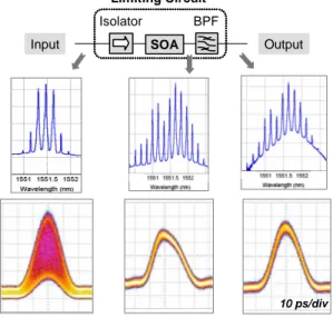
SOA BPF Isolator Limiting Circuit Input Output 10 ps/div
Fig. 2. Typical evolution of the optical spectrum and of the oscilloscope trace (in persistence mode) of an over-modulated 20 GHz pulse train inside the limiting circuit.
The bandwidth of such filter must be so large to select only part of the output spectrum. As it is reported in the following sections, this band-pass filtering process has a twofold action both on the output pulse shape and on the frequency response of the process. By selecting part of the chirped spectrum it determines the pulse shape and, at the same time, by removing part of the spectral components it speeds up the process [11]. To summarize those concepts we report in Fig. 2 an example of the evolution of the optical spectrum and of the corresponding pulse trace through the limiting circuit. In this case a 20 GHz input pulse sequence is affected by a certain amplitude modulation. After the SOA, the modulation is practically removed, but the pulses are distorted as a consequence of the spectral chirp. The output filter selects only part of the spectrum reformatting the pulses.
SOA Gain full recovery time
R2
R1
time G2
G1
Fig. 3. Behavior of the SOA gain recovery as a function of pulse repetition rate.
Following the simple physical description we introduced, the cut-off frequency in the response of the limiting function is related to the inverse of the SOA recovery time. Nevertheless, a significant limiting effect can be expected also in case of modulating frequencies exceeding the cut-off point. In this case the same effect with reduced strength is obtained thanks to the partial gain recovery due to ultra-fast carrier-carrier and carrier-phonon
scattering working at sub and picosecond time scale [12]. Moreover, considering the the SOA gain recovery due to the ultrafast effects, we expect the circuit still working even with pulse trains at repetition rates exceeding the cut-off frequency [12]. Indeed, because of pulse periodicity the present technique can work also in case of partial gain recovery. As it is depicted in Fig. 3, depending on the repetition rates (e.g. R1 < R2) the carrier density and the gain no longer fully recover before the arrival of the following pulses. Hence, the available gain depends on the repetition rate and decreases at increasing the rate (G2 < G1).
SOA PC 20-40 GHz Signal Generator IM EDFA (0.8 nm)BPF TL OI Limiting Circuit Test 100KHz-12GHz Waveform Generator IM BPF Att Pulse Generation Intensity Modulation
Fig. 4. Experimental set-up. TL: Tunable Laser, IM: Intensity Modulator, EDFA: Erbium Doped Fiber Amplifier, OI: Optical Isolator, SOA: Semiconductor Optical Amplifier, BPF: Band Pass Filter.
This suggests that pulse trains with repetition rate even exceeding 100 GHz could be managed although at the cost of a weaker limiting capability [12]. Finally, the last critical parameter of the scheme is the wavelength position of the output bandpass filter in respect to the input signal. Indeed, the combination of SOA and the filter provides a threshold-like input/output transfer function. We will see in the following how this transfer function depends on the offset of the filter with respect to the input wavelength. On the other hand, the filter position determines also the shape of the output pulses. We found that a good trade-off between the limiting effect and proper pulse shape can be obtained setting the filter maximum close to the input wavelength.
3. Experiment and discussion
The experimental set-up used for the power limiter characterization is reported in Fig. 4. An optical carrier at λ = 1551.5 nm was generated by a continuous wave tunable laser. The pulses were carved by means of an intensity modulator driven by an electrical waveform generator. We used a LiNbO3 Mach-Zehnder modulator to generate the 20 GHz pulse trains (having 20
ps duration), and an Electro Absorption Modulator for the 40 GHz case obtaining 6 ps-long pulses. The amplitude modulation was superimposed by means of an additional intensity modulator driven by a sinusoidal signal from a wide-band waveform generator. Both the modulation depth and the frequency of this over modulating signal were tuned by adjusting the modulator bias and changing the frequency of the electrical waveform generator. The two electrical waveform generators were free running (not synchronized each other) in order to have no fixed phase relation. This condition guarantees to have an effective over modulation also for the high frequencies (in the GHz range) that are comparable with the pulse repetition rate. The signal was then amplified by an erbium doped fiber amplifier and power controlled by means of a variable optical attenuator. The limiting circuit was composed by an optical isolator, an SOA and a 0.8 nm tunable band-pass filter.
Fig. 5. (a). Typical static transfer function of the limiting circuit at varying the output band-pass filter position. b) Detail of the transfer function.
The SOA was a polarization insensitive pigtailed device with 28 dB small signal gain, around 200 ps full gain recovery time and 6 dBm output saturation power at 200 mA driving current. The output signal was analyzed by usual test instruments. In order to characterize the circuit, we measured the input-output static transfer function for different filter positions, i.e., the output power of un-modulated pulses at various average input power values.
Fig. 6. AMR vs. SOA average input power for 20 GHz pulse trains overmodulated at 5 GHz at 50 and 80% modulation depths.
Those functions have been measured for 20 GHz pulses, but following from the physical description and the considerations given in section 2 (see Fig. 3) similar trends can be expected for the 40 GHz case. In Fig. 5(a) we report the normalized results. For all the filter positions it shows a threshold-like shape. The trend becomes sharper when moving the filter position from the red shifted part of the spectrum to the blue one. The same trend is apparent in the magnified detail of the diagram of Fig. 5(b). On the other hand, we observed significant pulse distortion for the blue shifted filter position. Hence, we found as optimal position (i.e. the one that yields the largest amplitude reduction with no significant pulse distortion) the one close to the input carrier wavelength. To quantify in an unambiguous way the amount of amplitude modulation reduction of the circuit, we introduce the amplitude-modulation-reduction (AMR) parameter. We defined it as the input/output attenuation (in dB) of the spectral component (on an electrical spectrum analyzer) at the modulating frequency. To study the circuit response as a function of the input power, we report in Fig. 6 the trend of the AMR parameter in case of 20 GHz pulses over-modulated using a 5 GHz sine-wave with 50 and 80% modulation depths. As expected, the AMR increases when increasing the SOA average input power and consequently the gain compression. The largest AMR value is obtained at 5 dBm average input power, which practically leads to a full gain compression (27 dB).
80% Mod. depth @ 200 MHz
20 ps/div
Input Output
b)
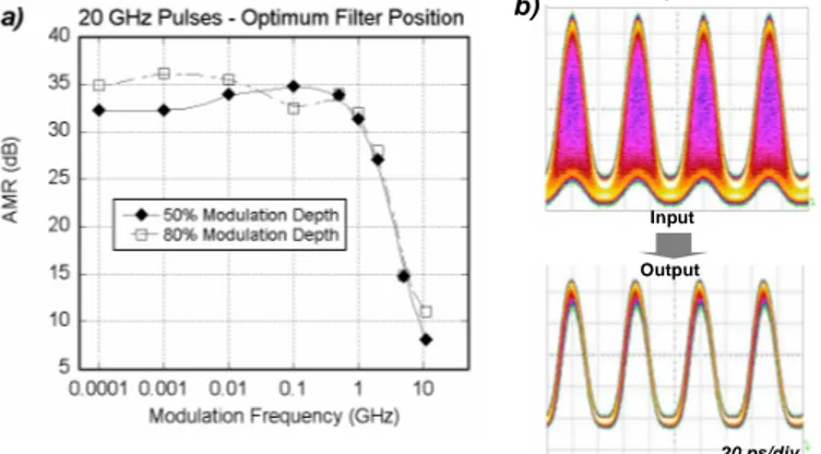
Fig. 7. (a). AMR vs. modulation frequency for 20 GHz pulse trains with 50 and 80% modulation depths. b) Input/output evolution of 80%-modulated pulse train (at 200 MHz modulation frequency).
The most important characterization in order to determine the field of application of the technique is the study of the frequency response of the circuit. We performed this characterization for the 20 and 40 GHz cases at sweeping the over-modulation frequency on very large intervals ranging from 100 kHz to 10 GHz and 25 GHz, respectively. Fig. 7(a) reports the results for the case of 20 GHz pulse trains. We measured the AMR of signals with 50 and 80% modulation depths for over modulating frequency swept from 100 kHz to 10 GHz while fixing 5 dBm average input power. We found in both cases a very large AMR in the range 32-36 dB from 100 kHz up to 1 GHz. The cut-off point in the response is around 3 GHz but, still 10 dB AMR is obtained up to 10 GHz. This is in good agreement with the qualitative physical description we draft in section 2. The cut-off frequency is clearly related to the inverse of the SOA recovery time (for this SOA we measured around 200 ps recovery time) and we found a residual limiting effect due to the ultrafast gain recovery. Moreover the cut-off frequency is lower than the pulse repetition rate and this agree with the statement that the technique works with partial gain recovery. We show the large effectiveness of the scheme in Fig. 7(b) reporting the input/output oscilloscope traces of a signal with 80% over modulation at 200 MHz (here and in the following figures we used a 53 GHz opto-electric converter and an ultra-stable time reference trigger). A correspondent value of 35 dB AMR completely removes any amplitude modulation without introducing any distortion on the pulse shape. After this characterization, we studied the way in which the filter affects the frequency response (sliding its position on the red-chirped part where we found no pulse distortion). In Fig. 8(a) we report the frequency dependence of the AMR in case of a signal with 80% modulation-depth and for various filter configurations: optimal, red-shifted and without filter condition.
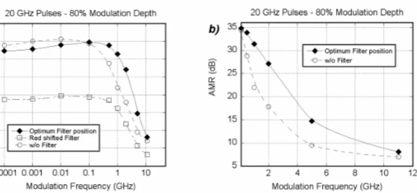
Fig. 8. (a). AMR vs. modulation frequency for 20 GHz pulse trains with 80% modulation depth with and without output filter. b) Detail in linear scale.
While the red-shifted filter configuration shows a quite lower AMR at all frequencies (in respect to the optimized filter condition), the filter benefit in respect of the no filter configuration is more pronounced at high frequencies. As can be observed in Fig. 8(b), the filter, besides preserving the pulse shape, significantly increases the cut-off frequency speeding up the limiting process for frequencies in the GHz range. This effect can be extremely useful in applications such clock recovery circuits for high bit rate signals, where significant pattern modulations related to long zero sequences may arise in the GHz range [6]. The frequency response of the circuit for 40 GHz pulse trains is reported in Fig. 9(a) for conditions similar to the 20 GHz case, i.e., 50 and 80% modulation depths and 5 dBm average input power. As expected from the considerations made in section 2, at increased repetition rate we find a reduction of the strength of the limiting effect. We found an AMR in the range 25-33 dB from 100 kHz up to 1 GHz, a similar cut-off point at a few GHz, and, still around a 10 dB AMR flat response for modulating frequencies up to 25 GHz.
80% Mod. depth @ 100 kHz
10 ps/div
Output Input
b)
Fig. 9. (a). AMR vs. modulation frequency for 40 GHz pulse trains with 50 and 80% modulation depths. b) Input/output evolution of 80%-modulated pulse train (at 100 kHz modulation frequency).
In Fig. 9(b) we report, as an example, the input/output traces of 40 GHz pulses that are 80% overmodulated at 100 kHz. In this case the AMR is around 27 dB and it has the effect to completely reshape the pulses.
Fig. 10. Comparison of the AMR response in the GHz range with and without output filter.
The comparison in linear scale of the high frequency response for 80% modulation depth in the optimum and without filter cases is reported in Fig. 10. Also here, clear improvement of the AMR can be addressed to the spectral selection of the output signal operated by the filter.
Fig. 11. AMR vs. modulation depth for 20 and 40 GHz pulse trains at 5 GHz overmodulation frequency.
We characterized the limiting effect also as a function of the modulation depth. The results for 20 and 40 GHz pulses are summarized in Fig. 11. We fixed the modulating frequency at 5 GHz and adjusted the modulation depth changing the bias of the second intensity modulator. We found that the AMR response trend is similar for both cases and, as expected, it is larger for the 20 GHz case. It is nearly flat and starts to decline once exceeded the 80%. According with the thresholding description, this indicates that the efficiency of the effect reduces when the modulation depth is so large that the lowest pulses in the sequence start to approach the threshold level. We report in Fig. 12 two examples at 40 GHz that clearly show the effectiveness of the scheme in extreme cases. In Fig. 12(a) we show the traces of a very deep modulation (86%) at 5 GHz, which exceeds the flat response part of Fig. 11.
86% Mod. depth @ 5 GHz 10 ps/div Output Input a) 40 GHz Output Input 10 ps/div 58% Mod. depth @ 25 GHz b)
Fig. 12. Input/output evolution of 40 GHz pulse trains modulated with a) 86% modulation depth at 5 GHz; b) 58% modulation depth at 25 GHz.
The output signal shows that a significant, yet not complete, limiting effect still occurs, reducing the modulation to around 52%. In Fig. 12(b) we report the case of a significant modulation (58%) at a very high frequency (25 GHz). We found a quite good output signal with around 20% residual modulation.
In order to further characterize the filtering effect both on the shape of the output pulses and on the efficiency of the effect, we performed a systematic study using 40 GHz pulse trains for a fixed over-modulation condition (80% depth at 100 MHz). The results are reported in Fig. 13. We recorded both the AMR and the pulse shape while sliding the position of the output filter. We observed that moving from the red to the blue-shifted side, the AMR significantly increases at the expenses of pulse shape degradation. When the filter selects the red-shifted part of the spectrum the output pulses are shorter and better shaped (so that pulse compression can potentially be obtained [13]), but with a lower limiting effect (note the residual amplitude modulation on the pulse in the inset).
5 ps/div 5 ps/div 5 ps/div Red Blue Center
Fig. 13. AMR vs. filter detuning for 40 GHz pulse trains 80%-modulated at 100 MHz. In the insets, examples of corresponding oscilloscope traces.
Symmetric pulses having larger AMR factors are obtained for filter positions closed to the center input wavelength, whilst the largest AMRs result for blue-shifted positions. In this last case distortions of the pulses and extinction ratio degradation are apparent. Following from those considerations, we see that we can balance in a very simple way (tuning the filter position) the strength of the limiting effect and the quality of the output pulses. This means that this limiting circuit can be flexibly adapted depending on the application.
Fig. 14. Comparison of the Single Side Band Noise Spectrum of 20 GHz pulse train without overmodulation at the input and output of the limiting circuit.
Finally, to analyze the ultimate limiting capability of the circuit, we performed an extremely sensitive characterization of the effect by studying the input/output phase noise evolution of an un-modulated 20 GHz pulse train. The results are reported in Fig. 14. We compare the Single Side Band (SSB) spectrum around the 20 GHz electrical spectrum clock line for input un-modulated and output pulses. This SSB spectrum contains the phase noise contributions due to amplitude and time jitter of the transmitter [14]. The plots clearly show an improvement of the signal phase noise also in this limit case. In detail, there is a slight reduction of the phase noise at any frequency with a significant effect (more than 10 dB) in the range 20 to 100 kHz.
4. Conclusion
In this work we experimentally characterized a very simple and flexible power limiting circuit made by a saturated SOA and a band-pass filter. We measured the amount of amplitude modulation reduction that the circuit produces working on 20 and 40 GHz over-modulated pulse trains (at varying the modulation frequencies and the modulation depths). We showed that this circuit definitely acts as a high pass filter with a cut-off frequency of around 3 GHz. Nevertheless, a modulation reduction factor of around 10 dB have been measured at much higher frequencies due to the fast recovery dynamics in the semiconductor material. This guarantees operation well beyond the cut-off frequency. Moreover, we believe that using novel quantum dot based SOAs [15] showing ultrafast recovery time (<5ps) it is possible to realize simple limiting circuits having ultra-large cut-off frequencies (> 100 GHz) and working with repetition rates exceeding 200 GHz [15].
Acknowledgment
This work was partially supported by the European Commission FP6 program (Integrated Project NOBEL II).