CONTENTS
PRELIMINARY REMARK ... 1
PART I
1 INTRODUCTION ... 31.1 BIOSENSOR DESIGN AND TEST ... 5
1.1.1 Biosensor architecture ... 6
1.1.1.1 Fluid carrier ... 8
1.1.1.2 Electrical interface ... 9
1.1.2 System architecture ... 9
1.2 CELL DELIVERY AND RECOVERY IN MICROWELLS ... 11
1.2.1 CellJet microdispenser ... 12
1.2.2 Commercial piezoelectric jetting device ... 12
1.2.3 Cell handling with a machined micropipette ... 13
1.3 BIOSENSOR TECHNOLOGY AND MANUFACTURING ... 15
1.3.1 Materials selection ... 16
1.3.2 Lab-On-Substrate manufacturing process flow ... 16
1.3.2.1 Lamination... 17
1.3.2.2 Microwell and via formation ... 18
1.3.2.3 Via metallization ... 18
1.3.2.4 Funnel ... 19
1.3.3 Hydrophobic / hydrophilic surface modifications ... 19
2 MATERIALS AND METHODS ... 21
2.1 MATERIALS ... 21
2.1.1 Tested materials for biosensor manufacturing ... 21
2.1.2 Cell lines and culture conditions ... 25
2.1.3 Compounds used to induce erythroid differentiation in K562 ... 25
2.2 METHODS ... 26
2.2.1 Analysis of in vitro cell growth ... 26
2.2.2 Erythroid differentiation of K562 cells ... 26
2.2.3 CTL-mediated LCL lysis: chromium release assay ... 27
2.2.4 Cytokine profiles ... 27
2.2.5 RNA isolation ... 28
2.2.6 Real-time quantitative RT-PCR ... 28
3 AIMS ... 30
4 RESULTS ... 32
4.1 IDENTIFICATION OF BIOCOMPATIBLE MATERIALS FOR BIOSENSOR MANUFACTURING ... 32
4.1.1 Effects of materials on cell growth ... 35
4.1.2 Effects of materials on erythroid differentiation ... 39
4.1.3 Effects of materials on cytokines release by IB3-1 cells ... 40
4.1.4 Effects of materials on CTL-mediated lysis of LCL cells ... 41
4.2 BIOSENSOR CHARACTERIZATION ... 42
4.2.1 Beads, cells and cells group levitation and trapping ... 42
4.2.2 Analysis of cell to cell interaction ... 43
4.2.2.1 Evaluation of CTL mediated lysis ... 45
4.3 BIOTECHNOLOGICAL SENSOR VALIDATION ... 48
4.3.1 Isolation and in vivo expansion of single cells ... 48
4.3.2 Biological characterization of isolated clone ... 49
4.3.3 Analysis of gene expression after single cell manipulation ... 51
4.3.4 Comparison between biosensor platform and BioStation ... 52
5 DISCUSSION ... 55
PART II
1 INTRODUCTION ... 601.1 IMMUNE SYSTEM ... 60
1.1.1 T lymphocytes ... 61
1.1.2 Proteasome and antigen processing ... 62
1.1.3 MHC class I molecules ... 64
1.1.4 Viral and tumor escape mechanisms ... 66
1.2 EPSTEIN BARR VIRUS ... 67
1.2.1 EBV infection ... 68
1.2.1.1 Latent infection ... 69
1.2.1.2 Lytic infection ... 69
1.2.2 EBNA1 protein ... 71
1.3 EBV ASSOCIATED MALIGNANCIES ... 73
1.3.1 Burkitt‟s lymphoma ... 74
1.3.2 Hodgkin's lymphoma and nasopharyngeal carcinoma ... 75
2 MATERIALS AND METHODS ... 76
2.1 MATERIALS ... 76 2.1.1 Cell lines ... 76 2.1.2 Synthetic peptides ... 76 2.2 METHODS ... 77 2.2.1 Proteasomes purification ... 77 2.2.2 Enzymatic assays ... 77 2.2.3 Peptide degradation ... 78
2.2.4 Western blot assay ... 78
2.2.5 Preparation of antigen-presenting cells ... 78
2.2.6 Generation of memory CTL cultures ... 78
2.2.7 Cytotoxicity assay ... 79
2.2.8 IFN- ELISPOT ... 79
2.2.9 Immunofluorescence detection of HLA-ABC molecules ... 80
3 AIMS ... 81
4 RESULTS ... 82
4.1 IMMUNE RECOGNITION AND EBNA1 DERIVED EPITOPE PRESENTATION IN LCL AND BL CELLS ... 82
4.1.1 Identification of a new EBNA1 epitope ... 82
4.1.2 Induction of EBNA1specific memory CTL responses directed to the HLAB35 and -B53-presented HPV CTL epitope ... 85
4.2 DIFFERENCE IN ANTIGEN PROCESSING MACHINERY BETWEEN LCLs AND
BLs ... 89
4.2.1 Expression of HLA class I and TAP molecules ... 89
4.2.2 Expression and activity of proteasomes in LCL and BL ... 91
4.3 MODULATION AND INDUCTION OF BLs RECOGNITION BY HPV-SPECIFIC CTL ... 94
4.3.1 Evaluation of the effect of the Gly-Ala repeat domain on HPV-mediated lysis in BL . 94 4.3.2 Modulation of antigen processing affects HPV epitope presentation in BL cells ... 95
4.3.3 In vitro generation of HPV epitope by proteasomes isolated from BLs ... 96
5 DISCUSSION ... 98
REFERENCES ... 102
ABBREVIATIONS ... 109
PUBLICATIONS ... 111
PRELIMINARY REMARK
PRELIMINARY REMARK
While conventional chemotherapy and radiation therapy have improved the survival of many cancer patients, there are still major disadvantages associated with these treatments such as high toxicity and drug-resistance. The possibility to manipulate the immune system to recognize and kill tumor cells is very attractive despite numerous obstacles remaining to be overcome, such as tolerance and tumor escape. In particular, the ability of the immune system to seek out and destroy disseminated micro-metastases in a specific way makes immunotherapy an attractive alternative or complement to conventional therapies. Nevertheless today other unconventional technologies have reached many progresses, in particular the analysis and monitoring of single cell-to-cell interactions and the capability of individually controlling single cells have become of interest in different areas of life sciences, ranging from immunotherapy and cancer research to rare cell identification and isolation. These new technologies in combination with progresses reached in anti-tumor vaccines could be useful to identify, understand and improve immune T cell responses against tumor antigen and the sensitization of tumors to T cell effector mechanisms for a more efficient immunotherapy.
In particular, this thesis focuses on two tumor immunotherapy issues:
1) design, realization and validation of innovative Lab-on-a-chip devices for immune system study, that allow single tumor cell and effector cells interaction, detection and isolation;
2) identification of molecular mechanisms that prevent Burkitt‟s lymphoma recognition by T cells and study of their potential correction by specific treatments. The main goal of this study remains indeed the evaluation of integrated strategies for immunotherapy development enhancing for malignancies treatment.
Part I INTRODUCTION
1 INTRODUCTION
A Lab-on-a-chip (LOC) is a device that integrates one or several laboratory functions on a single chip of only millimeters to a few square centimeters in size. LOCs deal with the handling of extremely small fluid volumes down to less than pico liters. These devices are a subset of MicroElectroMechanical systems devices (MEMS) and often indicated by "Micro Total Analysis Systems" (µTAS) as well. In particular often LOC integrates microfluidics and electronics on the same platform. Microfluidics is a broader term that describes also mechanical flow control devices like pumps and valves or sensors like flowmeters and viscometers. However, strictly regarded "Lab-on-a-Chip" indicates generally the scaling of single or multiple lab processes down to chip-format, whereas "µTAS" is dedicated to the integration of the total sequence of lab processes to perform chemical analysis. The term "Lab-on-a-Chip" was introduced later on when it turned out that µTAS technologies were more widely applicable than only for analysis purposes. Although the application of LOCs is still novel and modest, a growing interest of companies and applied research groups is observed in different fields such as analysis (e.g. chemical analysis, environmental monitoring and medical diagnostics) but also in synthetic chemistry (e.g. rapid screening and microreactors for pharmaceutics).
Besides further application developments, research in LOC systems is expected to extend towards downscaling of fluid handling structures as well, by using nanotechnology. Sub-micrometre and nano-sized channels, single cell detection and analysis, and nano-sensors, might become feasible, allowing new ways of interaction with biological species and molecules. The development of Lab-on-a-chip devices for biomedical applications, including manipulation of single cells, is
INTRODUCTION Part I
an exciting new research field requiring strict collaboration between electronic engineers and biologists1-10. In the past few years, printed circuit board (PCB) technology, that can be used for Lab-on-a-chip devices producing, has reached a resolution of tens of micrometers, which is enough for many microfluidics applications11-14. The main limitation of this approach in biomedical applications remains constituent materials biocompatibility. Recently the range of materials for PCB technologies has been extended. Most of them have already been developed for flex circuits and have rapidly become an industrial standard. Cost-effective technologies have also been proposed by introducing additional preparatory steps15-16 or by testing corrosion-resistant materials (like aluminum) in standard PCB processes17. The use of these „„board technologies‟‟ is particularly relevant to the development of microtiter plates with sensoring and actuating features that allow fast, parallel manipulation and analysis of biological samples18-20. The adaptation of standard PCB processes, which ensure low production costs and large-scale development, may here boost progress in the design of many disposable applications. Lab-on-a-chip technology may soon become an important part of efforts to improve global health particularly through the development of point-of-care testing devices21. Despite the first LOC analysis system was
developed in 1975 by S.C. Terry, Stanford University (it was a gas chromatograph), only at the end of the 1980s, and beginning of the 1990s, the LOC research started to seriously grow as a consequence of few research groups in Europe developing micropumps, flowsensors and concepts for integrated fluid treatments for analysis systems. A big boost in research and commercial interest came in the mid 1990‟s, when µTAS technologies turned out to provide interesting tooling for genomics applications, like capillary electrophoresis and DNA microarrays.
Part I INTRODUCTION
1.1 BIOSENSOR DESIGN AND TEST
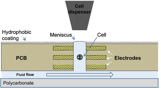
The idea of this project is to implement a microwell array using printed circuit board (PCB) technologies for the construction of the biosensor. Each microwell integrates actuation and sensing features by electrodes realized as structured conductor lines. The envisioned structure that is used for determining the cell-cell interaction by means of impedance change maintains the cells in equilibrium and traps them through dielectrophoresis forces (DEP). Figure 1 shows the sensor principle, but for the final device additional features will be added to the structure. Cells medium solution will flow from the bottom side into the microwells. Furthermore, a hydrophobic coating on PCB top will ease cell positioning into the microwells. Ultimately, the platform developed within the project, as shown in Figure 2, consists of an orderly matrix of up to thousands of microwells where living cells can be deposited and where microfluidics and electronics are integrated in a high-density circuit board.
Figure 1. Biosensor principle, schematic cross section. This biosensor represents a novel concept
of active microwells based on cylindrical wells able to vertically trap and control single particles by means of negative dielectrophoresis. The device is fabricated by drilling through holes on a solid substrate with metals layers, forming three annular electrodes within the well. A channel under the device provides a fluid flow filling the microwell by capillarity and cells or particles are delivered from the top by a microdispenser.
Polycarbonate Meniscus Electrodes Cell dispenser Hydrophobic coating PCB Fluidflow Cell Polycarbonate Meniscus Electrodes Cell dispenser Hydrophobic coating PCB Fluidflow Cell
INTRODUCTION Part I
The microwells are monitored by an external microscope, the electronics allow to control the biosensor electrodes, necessary to DEP forces induction, and to perform impedance measurements. The key point of this technology is that each microwell can force contact between individual cells, and detect consequences of these interactions.
Figure 2. Example of matrix with up to thousands of microwells and a small assembled biosensor
prototype with microfluidics and electronics integrated.
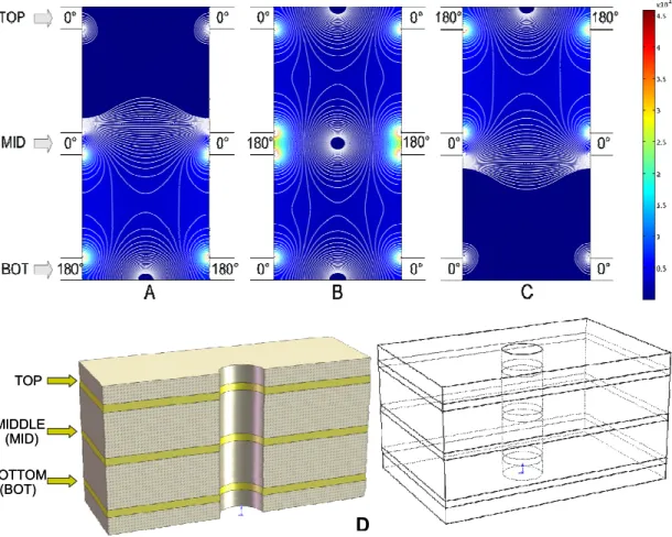
1.1.1 Biosensor architecture
Each microwell contains, as previously mentioned and as shown detail in Figure 3D, three annular electrodes at the top, middle and bottom levels (TOP, MID and BOT electrodes); by applying them a sinusoidal signals at frequencies ranging
from 100 kHz to 1.5MHz and amplitudes between 2V and 7V the microwell levitates the cells keeping them in the center of the structure. All possible configurations are obtained by applying the same sinusoidal signal on two electrodes and a counter-phase signal to the third one (Figure 3). The trap configuration is achieved by phase-shifting the MID electrode, thus creating an almost spherical cage at the level of the MID electrode and in the horizontal center
Part I INTRODUCTION
of the microwell. To guarantee this shape, the distance between TOP/MID and MID/BOT electrodes must be equal to the microwell diameter. Figure 3B shows a contour plot of the mean square electric field for a 2D structure representing a vertical cross section along one of the diameters of the hole. The reference particle for these simulations is a polystyrene bead. As it can be noticed in Figure 3B, the trap mode also creates a semi-spherical cage on the top side of the microwell, thus preventing a particle dispensed from the top from entering the well. A different electrode polarization scheme is then used to create a load configuration by applying the counter-phase signal on BOT electrode (Figure 3A), thus creating an electric field minimum, in the region above MID electrode.
Figure 3. 2D contour plot of mean square electric field on the vertical plane of a microwell. Load configuration (A) trap configuration (B) and eject configuration (C) are obtained by applying a 180° phase-shifted signal on Bottom (BOT), middle (MID) and TOP electrodes respectively and a 0° phase-shifted signal on the two remaining electrodes. (D) 3D views of the microwell; each microwell consists of a hole drilled on a flexible PCB substrate containing three annular electrodes (Top, Middle, Bottom).
TOP MIDDLE (MID) BOTTOM (BOT) TOP MIDDLE (MID) BOTTOM (BOT) D
INTRODUCTION Part I
Finally, the eject configuration (Figure 3C) opens the cage from the bottom, allowing particles to be removed from the microwell. When implementing microwell arrays, independent addressing of single microwells is possible by changing the phases of the applied signals. An important consideration for cells controllability is related to the electrodes thickness, with particular reference to the middle electrode. As shown in Figure 3B, the region close to middle electrode has two electric fields maxima corresponding to the electrode edges, while in the middle region the electric field becomes null. As a consequence, the effect of the middle electrode to repel a particle towards the central region in negative dielectrophoresis (nDEP) conditions is reduced for particles with a small size compared to the electrode thickness. These particles, in fact, will find a region corresponding to the level at the center of the middle electrode where the horizontal DEP force becomes null or small.
1.1.1.1 Fluid carrier
Regarding the biosensor microfluidic, to provide a fluid flow to fill microwells and change the supernatant, a fluid carrier was created by structuring polycarbonate sheets and sealing them with silicone gaskets (Figure 4A). The carrier includes a chamber with height of 2mm, a volume of 4ml and a fluid inlet and outlet on two sides, providing fluids to microwells. Spring-loaded connectors were integrated to provide the signals to microwells (Figure 4B).
A B
Figure 4. (A) Cross section of packaged system including the
microwell array and the fluid carrier. (B) Photograph of a prototype
A B
Figure 4. (A) Cross section of packaged system including the
Part I INTRODUCTION
1.1.1.2 Electrical interface
In order to send electrical signals to the biosensor, a PCB board (named “PCB Host”) was realized (Figure 5A). The board is equipped with different connectors arrays and when the fluid carrier is positioned on the board the electrical contact are allowed (Figure 5B). In particular electrical signals for electrode polarization were generated by a multifunction synthesizer (Hewlett-Packard 8904A, Palo Alto, CA). The two sinusoidal signals have a frequency of 600 kHz, an amplitude between 0.2V and 0.7V, a programmable phase shift and were amplified by 10 times on a custom circuit, thus providing a final amplitude between 2V and 7V.
Figure 5. (A) Picture of “PCB Host” board, a red arrow indicates where fluid carrier will be
positioned on the board (B) Picture of fluid carrier assembled on the “PCB Host” board.
1.1.2 System architecture
At the end, the biosensor considered in this thesis, is a fully automated system that integrates optical observation of microwells, alignment of target microwells beneath the microdispenser, automated motion, microfluidic handling and image/video capturing. Optical observation from the top of the microwell was performed by a fluorescence microscope (Nikon Eclipse 80i, Tokyo, Japan)
A B
INTRODUCTION Part I
equipped with a Nikon DXM1200 digital camera. Precise positioning within the micron-range of the biosensor under the microscope or under the microdispenser was made with an XYZ motorized microscope stage (Märzhäuser Wetzlar, Steindorf-Wetzlar, Germany). A fluid flow in the channel beneath the microwells was provided by a KDS-210 syringe pump (KD Scientific, Holliston, MA). All system parts were controlled by a set of modules implemented in LabView software (National Instruments, Austin, TX) to achieve complete automation of experimental procedures. The complete system architecture and its electrical and fluidic interfaces were specifically designed to maintain an easy way to disassemble the package, to remove the biosensor when necessary, replacing it with a new one and to perform the required cleaning procedures. A complete system scheme is reported in Figure 6, while Figure 7 shows its corresponding 3D view.
Figure 6. System diagram.
Microscope control Control electronics Fluidic (pumps) Dispencer control hardware Cameras PC (Labview) Fluidic cariers and electronics interface Biosensor Microscope Micro dispencer
Part I INTRODUCTION
1.2 CELL DELIVERY AND RECOVERY IN MICROWELLS
Equipments and procedures for depositing cells into biosensor microwells, as well as for recovering specific cells from selected microwells, were also developed inside this project. In particular to identify the best and most suitable dispensing technique three different dispenser system were investigated:
1.2.1) CellJet microdispenser. developed at Biochips Laboratory in CEA; 1.2.2) a commercial piezoelectric jetting device;
1.2.3) cell handling with a machined ceramic micropipette.
The instrumentation for cell handling includes some mechanical supporting structures, such as, motorized stages, pressure control, optical devices, software, and development of operational loading methods (Figure 8).
INTRODUCTION Part I
1.2.1 CellJet microdispenser
In CellJet microdispenser, the cells are introduced into a microfluidic chip, transported and lined up along a microchannel, and detected by microelectrodes. For achieving cell dispense, some ~1 µL droplets are generated by a miniaturized solenoid valve so that the cells are brought out through the orifice of the microchannels. The cell-containing droplets are finally collected and absorbed by the microwell of the biosensor placed underneath (Figure 9). Deposited cells were proved to enter and pass through the microwells within few minutes. A software program for the cell microdispenser was developed, it automatically drives the CellJet microdispenser. Moreover, electrical profiles of cells flowing through the microfluidic chips were investigated to parameterize cell dispense.
1.2.2 Commercial piezoelectric jetting device
In second analysis a commercial piezoelectric dispenser was also employed for cells depositing. As the diameter of human cells is about 20 µm, a dispenser with an orifice of 60 µm was chosen. The formed droplet has generally a diameter slightly larger than the orifice diameter, e.g. 65 µm in diameter which results in an
Microdispenser Jet
Figure 9. Spot dispensed onto a microwell by the CellJet microdispenser. The jet is narrow and
very straight, allowing the spot to be located in the near vicinity of the microwell. The spot is absorbed by the microwell within seconds or minutes according to the fluidic resistance of the underneath microwell.
Part I INTRODUCTION
individual ejected volume of ~140 pL. A droplet generation requiring no pressure controller was implemented, and drivers using LabView software were programmed for controlling the electronic triggering of droplet jetting. Two modes of dispense were developed: a „stop-on-spot‟ mode where the biosensor is moved and stopped under the microdispenser for dispense; and a „in-fly ejection‟ mode where dispense is very rapid so that the ejected droplets can reach the underneath microwell while the biosensor is still moving at a constant velocity. Heterogeneity of the number of deposited cells were generally observed, which is likely due to sedimentation of cells upstream of the dispenser orifice. A classical limit dilution strategy, in which a low concentration of cells is introduced so that the total volume of cells statistically contains one single cell, was successfully investigated to resolve this heterogeneity.
1.2.3 Cell handling with a machined micropipette
Finally, a micropipette was machined from a capillary made in alumina (Al2O3) and
toughened by zirconia (ZrO2), as shown in Figure 10. This material is very
resistant to mechanical shocks and thus is tolerant to abrupt contacts with the microwell walls. Moreover, the micropipette extremity was micromachined for providing inner and outer diameters of 56 µm and 150 µm respectively. As a result, the pipette can handle T, B lymphocytes and NK cells of ~8 µm in diameter, and tumor cells of epithelial origin and melanomas of ~16 µm in diameter, as well as penetrate into the conical entrance of the microwell (300-400 µm in diameter) and collect the upper fraction of the microwell liquid. The microwell is supplied with liquid from the bottom fluidic chamber, and thus a prolonged aspiration of liquid by the micropipette is possible by continuous replacement of liquid during pipetting. Eventually, the meniscus height in the
INTRODUCTION Part I
microwell can be increased beyond the microwell border by controlling the pressure inside the fluidic chamber. Meniscus upward movements can form a droplet above the microwell which facilitates the contact between the pipette and the liquid and this aids the aspiration process. The ultrathin micropipette can be used both for depositing cells and for aspirating cells from microwells. By reversing the flow direction in the micropipette, the volume of liquid previously aspirated by the pipette can then be deposited into another microwell.
Ceramic micropipette Microwell with a going-out meniscus Ceramic micropipette Microwell with a going-out meniscus
Figure 10. Handling of cell-containing liquid with a micromachined ceramic micropipette. The
micropipette inner channel can be seen by transparency. A meniscus is formed above the microwell by enhancing pressure inside the fluidic biosensor chamber.
Part I INTRODUCTION
1.3 BIOSENSOR TECHNOLOGY AND MANUFACTURING
A key point in this innovative device is the fabrication technology of the microwell array. Several technologies for microfluidic device fabrication and packaging have been proposed to integrate sensing capabilities and electrical interfaces into a single device. All these approaches require complex steps or expensive facilities, and mostly are useful for prototyping only. In opposition to existing technologies, the biosensor developed within this project needs to be low cost and disposable to be applicable for the intended purpose. Due to these requirements, standard printed circuit board (PCB) manufacturing processes were selected as base technology. In addition to be a low cost mass production tool, it allows the realization of fine structures and vias with feature widths below 100 µm. Drawback of this technology is the default use, as conductive substrate, of non-biocompatible materials as e.g. copper (Cu). Therefore, the first task was to identify a list of materials which could be processed with standard PCB technologies as substitutes of non-biocompatible materials. As a consequence with the hypothetic use of new materials and new material combinations also processes as lamination, conductor line structuring, microwell drilling, via formation and via metallization need to be developed or at least adapted. Additionally surface modifications have to be developed for the sensor manufacturing. The bottom side of the microwell sensor should have a hydrophilic surface for a bubble free wetting and flow of medium solution for the cells. On the other hand the top side of the sensor should have a hydrophobic surface for easier cell positioning into the microwell.
INTRODUCTION Part I
1.3.1 Materials selection
In standard PCB manufacturing process typically Resin Coated Copper (RCC) and glass fiber filled epoxy films are used. These materials are not applicable for the microwell array realization due to copper incompatibility and the poor processability of fiber filled epoxies by laser structuring. Standard copper technology in combination with biocompatible metallization on top does not work due to the proposed manufacturing technology of the device (smearing of Cu particles during via drilling is contaminating also dielectric surfaces) and the metallization growth of an additional layer. Thus, no safe biocompatible device could be achieved using such a process combination. Therefore, new dielectric materials have to be evaluated in combination with biocompatible metal layers. As possible metals for conductive layer formation palladium, aluminum and gold were taken into account. Pyralux (Py), a B-staged modified acrylic adhesive, in combination with Polyimide, printable epoxies and epoxy films with aramid fibers have been discussed as dielectric layers. For the realization of the final Lab-on-Substrate device also a hydrophobic / hydrophilic surface modification is needed, therefore, different coatings and modifications have to be evaluated.
1.3.2 Lab-On-Substrate manufacturing process flow
The starting process for PCB production, that will constitute biosensor heart/ physical support, is the lamination of the inner Aluminum–Pyralux–Polyimide layer. In sequential steps aluminum (Al) structuring is done by wet chemical etching followed by lamination of the next dielectric and metal layer. Final layer on top and bottom side is a Polyimide (PI) passivation. Microwells, through vias and blind vias are realized by laser drilling. The last process step would be the electroless metal
Part I INTRODUCTION
deposition for via metallization. Briefly, the general process sequence for Lab-On-Substrate manufacturing with standard technologies is shown in Figure 11.
Figure 11. PCB manufacturing process flow.
1.3.2.1 Lamination
A Lauffer vacuum laminating press was used for all lamination processes described. This press allows the lamination under vacuum with defined parameters as pressure, temperature and time. The lamination process starts with a drying step at 50 °C under vacuum without pressure. The following lamination steps under force, heating and vacuum are used to achieve homogeneous layer thicknesses and good adhesion between the different layers. In particular Figure 14 shows a cross section of a final laminated Al-Py-PI stack.
INTRODUCTION Part I
1.3.2.2 Microwell and via formation
Once obtaining laminated Al-Py-PI stack it is necessary to create via and microwell inside the support for the final device ideation (Figure 12A). In particular for this purpose an UV laser system is used and the drilling process is milling the material through the laser beam. A 60 µm via in a Al-Py-PI stack of 210 µm overall thickness is shown in Figure 12B as an example. Due to the different material properties of Pyralux and the PI layer, the resulting via diameter of these materials is often different. Vias in Pyralux are larger, possibly due to a combination of higher ablation rate and larger thermal shrinkage with this material. Another important and crucial aspect of this process is the protection of the substrate surface, since the material removed during the laser drilling process can be re-deposited and consequently contaminate the substrate surface.
Figure 12. (A) Schematic cross section of device where microwell, different material layer and vias
are shown (B) Picture of 60 µm via in Aluminum/Pyralux/Polyimide stack (Al/Py/PI).
1.3.2.3 Via metallization
An electroless Ni/Au process has been used to realize electrical connections between inner aluminum layers and solder able pads on top of the device. The basic process chain is a sequential treatment of the Al with different chemicals,
A B
A B
Part I INTRODUCTION
which are needed to apply the desired pretreatment to the pads, followed by the electroless Ni and immersion Au deposition.
1.3.2.4 Funnel
To get cell spotting into the microwells easier, a funnel has been projected above each microwell, therefore on top of the final metal layer two thick polyimide layers will be laminated. The polyimide will act as passivation on the metal structures and as a base for funnels. Funnels are mechanically drilled before the microwells are drilled by laser. An example of a microwell with funnel structure is shown in Figure 13.
Figure 13. (A) Picture of funnel realized by mechanical drilling in the final Polyimide top layer; (B)
Schematic microwell cross section where funnel is realized, different material layer assembled in final device are indicated in different colours.
1.3.3 Hydrophobic / hydrophilic surface modifications
Different hydrophobic/hydrophilic coatings on device have been investigated, for example, to ease cell positioning into the microwells or to ease flow inside biosensor microchannel. For these purposes, all materials used for device realization were characterized and classified according to their surface energy; in particular, contact angle measurement of different candidate materials were determined with test liquids bromonaphthalene (nonpolar), glycerol (slightly polar)
Polyimide 4 Semipermeable membrane PCB A B Polyimide 4 Semipermeable membrane PCB Polyimide 4 Semipermeable membrane PCB Polyimide 4 Semipermeable membrane PCB A B
INTRODUCTION Part I
and water (highly polar). It was found that the surfaces of both Polyimide and Aluminum must be treated to allow a designing of a hydrophilic/hydrophobic microfluidic network required for a successful operation of sensor devices. Other different surface modifications were considered e.g. fluoralkyl polymer, hydrocarbon polymer, octadecane thiol and SF6-plasma to increase hydrophobicity; and organic acids, O2-plasma and several polar silanes to
Part I MATERIALS AND METHODS
2 MATERIALS AND METHODS
2.1 MATERIALS
2.1.1 Tested materials for biosensor manufacturing
The materials under-test (Table 1) were embedded in standard multiwell plates for cell culture (Costar-Corning, USA) in which the biological experiments for biocompatibility were carried out.
Table 1. Complete list and abbreviation of tested materials.
Group Name Abbreviation
Me
tals
Copper Cu
Aluminum Al
Palladium Pd
Gold over Nickel Au over Ni
Gold over Palladium Au over Pd
Diele ctric s-adh es ive s Polyimide PI
Pyralux uncured Py uncured
Pyralux cured Py cured
Poly(dimethylsiloxane) PDMS
Polyurethane foil before lamination PF before lam
Polyurethane foil after lamination PF after lam
Polyurethane Powder PP
Epoxy cured Epoxy cured
Die Attach Film DAF
Aramid fiber cured Aramid fiber cured
Aramid fiber uncured Aramid fiber uncured
Tesa 4983 Tesa 4983 Tesa 4985 Tesa 4985 CMC 15581 CMC 15581 S u rf ac e tre atm ent
s Copper + Octadecanethiol Cu + ODT Palladium + Octadecanethiol Pd + ODT
Gold over Nickel + Octadecanethiol Au over Ni + ODT
Gold over Palladium + Octadecanethiol Au over Pd + ODT
Certonal FC-732 Certonal FC-732
Certonal FC-732 Tempered Certonal FC-732T
MATERIALS AND METHODS Part I
The materials, mostly foil, were cut by laser machining in round samples of 5.7 mm diameter for 96-well plates and 15 mm for 24-well plates. Blue film was used to cover the sample during the cutting preventing its surface contamination due to the melting materials produced by the laser process. The sample has been embedded in the well with a droplet of PDMS. It was dispensed in each well by an air pressured dispenser (EFD, USA) with a 0,020‟ tip (internal diameter; EFD Precision Tips, USA) applying a pressure of 1.5 bar for 2.3 s for a 96 well plates and 13.8 s for a 24 well plates. The dispensing parameters were defined by tuning dispensing time, fixed pressure and tip diameter. The covering of the sample edges was optically measured by a Wild H3Z microscope (Heerbrugg, Switzerland) equipped with a MFK II measuring system (Kappa, Germany) at different dispensing time for a 96-well. PDMS was partially dried for 5 minutes at 45°C after the dispensing. The round samples were deposited by a vacuum tip (EFD, USA) applying a light pressure. The protocol including dispensing, heating and sample deposition was repeat for each row of the multiwell plate. Finally PDMS was fully cured at 45°C for 24 h.
Aluminum (18 μm thickness, Al), Copper (136 μm thickness, Cu), Polyimide (100 μm thickness) were bought in foils and tested without any further process. In particular in this study materials will be referred as uncured (the material as delivered), b-stage (intermediate stage of the curing process) and cured (after complete processing).
In order to understand the possible effect of a non-complete curing of internal layers during lamination process, Pyralux LF0300 adhesive (DuPont, USA) and aramid fiber filled epoxy F161 (HEXCEL, California) were tested both as uncured and cured materials (Pyralux uncured or cured and aramid fiber uncured or cured). Similarly, Polyurethane films (TPU-4201, Epurex Films, Bayer MaterialScience, Germany) were tested either before and after the lamination process (PF before
Part I MATERIALS AND METHODS
lam and PF after lam), while a second type of Polyurethane (94AU925, Merkel Freudenberg Fluidtechnic, Hamburg, Germany) provided as powder (PP) was tested after lamination.
Aramid fiber filled epoxy was laminated following the curing cycle reported in its datasheet (Hexel, California).
Patternable Epoxy (SEMICOAT513E, Shin-Etsu Chemical Co. LTD., Japan) requires up to 150°C to be cured [60min, 100°C + 90 min, 150°C] (Epoxy cured). This temperature is not compatible with the multiwell plate made with Polystyrene, which glass transition temperature is 95°C. To overcome this limitation a film of epoxy, 100µm-thick, has been patterned on a support covered with cured Doubling silicone for dental copy (SUPERIUM Dubliersilikon, Weber Dental - Germany), cured, peeled out as a foil and cut by laser. The hydrophobicity of the Doubling silicone avoids the sticking of the epoxy film.
The Die Attach Film (DAF) is a polymer film (thickness 120 mm) consisting of a thermosetting and UV curable resin. This commercially available film could also be used for large-area lamination of different layers, as is needed in the case of a multilayer PCB.
Poly(dimethylsiloxane) (PDMS, Sylgard 184, DowCorning) was prepared mixing the two components of Sylgard 184 with a ratio of 1:10 for 5 minutes and degassed for 30 minutes at 0.1 bar (4 min were required to reach 0.1 bar), prepared according to previous study22, and cured in the well at 45°C overnight. Palladium (Pd) and Gold (Au) have been chemically deposited on copper substrates by electroless process. For Pd deposition, first Nickel (Ni) was deposited as adhesion layer (15 min, 90°C) followed by Pd activation (1 min, 55°C) and Pd deposition (30 min, 60°C). For Au deposition on Ni (Au over Ni), Ni was deposited as adhesion layer (15 min, 90°C) followed by Pd activation (1 min, 55°C) and Au deposition (30 min, 50°C). For Au deposition on Pd (Au over Pd), Ni
MATERIALS AND METHODS Part I
was deposited as adhesion layer (15 min, 90°C) followed by Pd activation (1 min, 55°C), Pd deposition (30 min, 60°C) and Au deposition (30 min, 50°C). The Cu substrates were cleaned in HCl 0.5% for 30 sec before the deposition, rinsing with DI-water and drying with nitrogen.
The acrylic adhesive transfer films Tesa 4985 and 4983 (Tesa tape, USA), with a thermal stability up to 200°C, and CMC 15581 (CMC technical tapes, Germany), with a thermal stability up to 130°C, have been prepared in multiwell plates. The tapes, protected on both sides by cover papers, have been cut in samples by laser. All the tapes are transparent and provide a permanent adhesion. The transfer tapes were stuck in the well and PDMS was manually dispensed to cover their edges and cured as for the other multiwell plates.
Certonal FC-732 was deposited filling the well for half of its volume for 5 min, rinsing with water and drying with a nitrogen flux at RT. Certonal was also deposited on an aluminum foil and tempered for 20 min at 150°C on a hotplate (Certonal FC-732T), after which it was cut by laser. A thin layer of Chemlease 41-90 (Chemlease) has been applied on an aluminum foil, tempered for 20 min at 150°C on hotplate and cut in samples.
The Au, Pd and Cu surfaces have been functionalized with 1-octadecanethiol (ODT) (Sigma-Aldrich) making it hydrophobic. Ethanol was deoxygenated with bubbling nitrogen for 1 h before using it as a solvent for thiols, but not purified further23 . The metal substrates, embedded in multiwell, have been cleaned with isopropanol for 2 h, rinsing with DI-water and ethanol before the thiol monolayer deposition (24 h at RT). ODT 1 mM has been prepared in ethanol. Any significant variation in the contact angle was recorded using piranha solution24 or plasma etching23 for the cleaning of the substrates. After the deposition, the samples were rinsed with ethanol and dried with a jet of high purity nitrogen.
Part I MATERIALS AND METHODS
Since all the surface treatments (Certonal, Chemlease and ODT) produce an hydrophobic behavior of the treated surface, the presence of these coatings was verified by measuring contact angle of the processed surfaces25. All materials
were UV-light sterilized before testing.
2.1.2 Cell lines and culture conditions
Lymphoblastoid cell lines (LCL) have been obtained after infection of human B-lymphocytes with B95.8 strain of Epstein-Barr Virus (EBV)26. LCL and the human erythroleukemia K562 cells27 were maintained in RPMI 1640 medium (Sigma-Aldrich, Milwaukee, Wisc., USA) at 37°C in a humidified 5% CO2 atmosphere,
supplemented with 10% fetal bovine serum (FBS; CELBIO, Milano, Italy), 100 units/ml penicillin and 100 g/ml streptomycin (Sigma-Aldrich, St.Louis, MO, USA). IB3-1 were cultured in LHC-8 (Gibco; Invitrogen, San Diego, CA) supplemented with 5% FBS. The other cell lines employed in this work such as 221 and 221-G1 lymphoblastoid cells, NKL and YTS natural killer-like cell line were provided by Regina Elena Cancer Institute, Rome.
2.1.3 Compounds used to induce erythroid differentiation in K562
Mithramycin (Sigma-Aldrich, St.Louis, MO, USA), cytosine arabinoside (AraC) (Sigma-Aldrich, St.Louis, MO, USA), and a C(5) modified uracil derivate30 (referred as AA55) kindly provided by Prof. R. Corradini (Department of Organic and Industrial Chemistry, University of Parma).
MATERIALS AND METHODS Part I
2.2 METHODS
2.2.1 Analysis of in vitro cell growth
For studying the effects on in vitro cell growth, with continuous incubation or after pulse incubation (60 minutes) with the materials, cells were seeded at the initial cell concentration of 30,000 cells/ml (K562 cells) or 50,000 cells/ml (LCL and IB3-1 cells), cultured in RPMI supplemented with IB3-10% FBS (or LHC-8 supplemented with 5% FBS for IB3-1) and the cell number/ml was determined using a model ZBI Coulter Counter (Coulter Electronics, Hialeah, FL, USA) after different days of cell culture.
2.2.2 Erythroid differentiation of K562 cells
The experimental protocols for analysis of the effects of the biomaterials on the erythroid differentiation were the following: (a) K562 cells were cultured to within biomaterial-treated 24-well plates for different days and treated with 25 nM mithramycin a powerful inducer of erythroid differentiation28 (continuous exposure); (b) K562 cells were exposed to the different biomaterials for 1 hour, then washed, sub-cultured in standard medium conditions and treated with 25 nM mithramycin for the following days (short exposure). The proportion of benzidine-positive cells was determined after 5 and 6 days of cell culture using a solution containing 0.2% benzidine in 5 M glacial acetic acid (10% H2O2)29.
Part I MATERIALS AND METHODS
2.2.3 CTL-mediated LCL lysis: chromium release assay
Monocyte-depleted PBLs from HLA-A2 positive blood donor were plated at 3,5x10⁶ cells per well in 24-well plates in RPMI 1640 containing 10% fetal bovine serum (FBS Hyclone; CELBIO, Milano, Italy) and stimulated with EBV nuclear antigen 3 (EBNA-3) SVR peptide (10 M). Cultures were restimulated after 7 and 14 days, and the medium was supplemented from day 8 with 10 U/ml rIL-2 (Chiron). On days 14 and 21, T cell cultures were tested for CTL activity using cytotoxicity assay. SVR-specific CTL cultures efficiently lysed SVR-pulsed human leukocyte antigen A2 (A2) positive LCLs, but did not lyse SVR-pulsed HLA-A2 negative LCLs (data not shown). Cytotoxic activity was tested by a standard 5h
51Cr-release assay31. Briefly, target cells were labeled with 0.1 µCi/106 cells of
Na251CrO4 for 90 minutes at 37°C and pulsed for 45 minutes with 10-5 M of peptide
at 37°C. Cells were then washed and used as targets at different effector : target (E:T) ratios. Percentage specific lysis was calculated as 100 x (cpm sample - cpm medium)/ (cpm Triton X-100 - cpm medium), where cpm is counts per minute.
2.2.4 Cytokine profiles
Cytokines in tissue culture supernatants released from IB3-1 under analysis, were measured by Bio-Plex cytokine assay (Bio-Rad Laboratories, Hercules, CA)32,33 as described by the manufacturer. The Bio-Plex cytokine assay is designed for the multiplexed quantitative measurement of multiple cytokines in a single well using as little as 50 µl of sample. In our experiments, we used the premixed multiplex beads of the Bio-Plex human cytokine 11-Plex Panel, which included eleven cytokines (IL-1alpha, IL-2ralpha, IL-3, IL-12, CTACK, GRO-alpha, ICA1, LIF, M-CSF, SDF-1alpha, TRAIL). Briefly, 50 μl of cytokine standards or samples (supernatants from treated cells) were incubated with 50 μl of anti-cytokine
MATERIALS AND METHODS Part I
conjugated beads in 96-well filter plates for 30 min at RT with shaking. Plates were then washed by vacuum filtration three times with 100 μl of Bio-Plex wash buffer, 25 μl of diluted detection antibody were added, and plates were incubated for 30 min at room temperature with shaking. After three filter washes, 50 μl of streptavidin-phycoerythrin was added, and the plates were incubated for 10 min at room temperature with shaking. Finally, plates were washed by vacuum filtration three times, beads were suspended in Bio-Plex assay buffer, and samples were analyzed on a Bio-Rad 96-well plate reader using the Bio-Plex Suspension Array System and Bio-Plex Manager software (Bio-Rad Laboratories, Hercules, CA).
2.2.5 RNA isolation
Total RNA was phenol–chloroform-extracted from cytoplasm of treated and untreated K562 cells28. All solutions were made in diethylpyrocarbonate (DEPC)-treated water. The extracted RNA was precipitated in two volumes of absolute ethanol and stored at −80 °C, washed once with cold 75% ethanol, dried and dissolved in DEPC-treated water before use.
2.2.6 Real-time quantitative RT-PCR
Quantitative real-time PCR assay of α-, β-, -, -, -, -globin mRNA and α-, β-, -, -, -, -globin transcripts have been carried out using gene-specific double fluorescently labelled probes in an ABI Prism 7700 Sequence Detection System version 1.7.3 (Applied Biosystems, Monza, Italy). The following primer and probe sequences were used: α-globin forward primer: 5‟-CAC GCG CAC AAG CTT CG-3‟, α-globin reverse primer: 5‟-AGG GTC ACC AGC AGG CAG T-CG-3‟, α-globin probe: 5‟-FAM-TGG ACC CGG TCA ACT TCA AGC TCC T-TAMRA-3‟; β -globin
Part I MATERIALS AND METHODS
forward primer: 5‟-CAA GAA AGT GCT CGG TGC CT-3‟, β -globin reverse primer: 5‟-GCA AAG GTG CCC TTG AGG T-3‟, β -globin probe: 5‟-FAM- TAG TGA TGG CCT GGC TCA CCT GGA C-TAMRA-3‟; -globin forward primer: 5‟-TGG CAA GAA GGT GCT GAC TTC-3‟, -globin reverse primer: 5‟-TCA CTC AGC TGG GCA AAG G -3‟, -globin probe: 5‟-FAM- TGG GAG ATG CCA TAA AGC ACC TGG-TAMRA-3‟; -globin (Applied Biosystems, Hs00426283_m1); -globin (Applied Biosystems, Hs00362216_m1) and -globin (Applied Biosystems, Hs00923579_m1). For real-time PCR, the reference gene was 18S; this probe was fluorescent-labeled with VIC (Applied Biosystems, Monza, Italy)34.
AIMS Part I
3 AIMS
The Cell-On-CHIp biosensor (COCHISE) for detection of cell-to-cell interactions is a specific targeted research project which addresses integrated systems for point-of-care diagnosis, monitoring, and drug delivery. This project is the first step of an activity aimed at the development of enabling micro-technologies to monitor physiological cellular interactions at single cell level with a high throughput. One of the primary applications of this technology is the immunological monitoring of anti-tumor vaccinations, singling out the rare effector cells (in the order of 1 cell among 1000 cells) that are actually active against tumor cells.
The first aim within the project was to develop an appropriate platform that combines microfluidics and electronics together and that consists in an orderly matrix of up to thousand microwells where living cells can be deposited. Secondly the aim of this thesis was to identify a correct protocol for biocompatibility analysis of materials that should be subsequently chosen for biosensor manufacturing. After biosensor assembling, with the most biocompatible materials, it has been necessary to test the platform from a functional point of view, in particular the third intention was the development of experimental cellular systems useful to validate the COCHISE platform. For this purpose several proofs were performed to trap before beads, cluster cells and single cells from different cell lines. After demonstrating that the biosensor was functional and allowed to trap and recover single cells we have set ourselves the objective to understand whether single cells manipulation was a not toxic procedure, determine if the manipulated cells maintained their biological activity and finally if gene expression remained unaltered. Since the main purpose of this research is the definition of new
Part I AIMS
therapeutic and diagnostic protocols for tumor immunotherapy, our next step was to apply our technology to the analysis of anti-tumor lytic effector cells.
In particular our aim was to demonstrate that this platform is suitable for detection and isolation of specific immune cells, that have shown, into the biosensor, ability to recognize and lyse tumor cells. On the other hand our purpose was also to identify and recover tumor cells that resist to CTL or NK lysis for further more detailed analysis and characterization from a biomolecular point of view, or to isolate rare steam cells. Ultimately the final goal was to develop a specific tool able to improve immune system response analysis in order to advance tumor immunotherapy.
RESULTS Part I
4 RESULTS
4.1 IDENTIFICATION OF BIOCOMPATIBLE MATERIALS FOR
BIOSENSOR MANUFACTURING
The first aim of this study was to determine the biocompatibility of materials employed for the COCHISE platforms fabrication. This objective is related to the concept that the manipulation of single cells requires that the employed materials are non-toxic and defined as biocompatible. For this purpose the foils of materials under testing were cut in round samples (see Figure 1A) by laser: 5.7mm of diameter for 96-well plate and 15mm for 24-well plate. A blue-foil were used to cover the material during the cutting, in order to prevent surface contamination caused by melted material particles. Then the sample were embedded in well bottom of a standard multiwell culture plate with a droplet of PDMS as reported in Figure 1B. The PDMS was dispensed in each well by an air pressured dispenser (EFD, USA) with a 0,020‟ tip applying a pressure of 1.5 bar for 2.3 sec for a 96-well plate and 13.8 sec for a 24-96-well plate.
Figure 1. Materials embedding in standard multiwell plate for biocompatibility tests. (A) Materials
are cut by laser in round samples and then (B) embedded with a PDMS droplet; PDMS was also used for covering the cut edges to prevent any contamination coming from the support material.
B A
Part I RESULTS
The dispensing parameters were defined tuning the dispensing time keeping fixed pressure and tip diameter. Subsequently, after the dispensing and the round samples deposition by a vacuum tip and applying a light pressure, PDMS was partially dried for 5 min at 45ºC. Finally the PDMS was fully cured at 45°C for 24h. An example of a 96-well plate and 24-well plate with embedded materials are shown in Figure 2. After obtaining the appropriate plates, biocompatibility tests were performed to identify suitable materials for biosensor construction. In particular we studied a significant number of materials, commonly used for the implementation of Lab-on-a-chip platforms, all materials tested are shown in Table 1. Biological tests were performed on several cell lines (e.g. as model of cells growing in suspension were chosen LCLs and K562 cells, while as model of attached cell cultures were chosen IB3-1 and rat hippocampal primary cells) and on different biological functions (e.g. cell growth, erythroid differentiation of K562 cells, CTL-mediated cell lysis and cytokine release by IB3-1 cells).
Figure 2. Materials embedding in standard
96- and 24-multiwell plates for biocompatibility tests.The materials, cut in round sample, were embedded in bottom well of a standard 96-and 24-multiwell culture plate with a PDMS droplet. Pictures of representative multiwell plates were assay have been performed are shown.
RESULTS Part I
TABLE 1. Complete list of tested materials.
Group Materials Comments and possible drawbacks Ref.
M
ETALS
Copper (Cu) Standard metal in a PCB; due to high chemical instability in wet environment is not used in bio-devices. 12
Palladium (Pd), Nickel (Ni), Gold (Au)
Applied with an electroless process to a copper substrate. 1735
Aluminum (Al)
Widely and cheaply available as a foil; potential substitute of copper in PCB process flows; few nanometers of its oxide self-passivate the aluminum surface making it stable in wet environments. This thin protective layer can be overcome in electrical measurements by increasing the signal frequency.
1925 35
DIELECTRICS
Polyimide
Used in the electronics industry for flexible PCBs or as a high-temperature adhesive; used as a substitute of the FR4 substrate material, typically used for rigid PCB devices.
1225 35
Pyralux
A B-stage acrylic adhesive, where B-stage means an intermediate stage in the cure reaction of a thermosetting resins. Used as an adhesive to create stacks of multiple dielectric and metal layers. Available in a wide range of thicknesses and in different forms: adhesive sheet itself, or coupled with polyimide.
2535
Polyurethane
Widely used as flexible and rigid foams, durable elastomers and high performance adhesives and sealants. Available either as powder and as films which can be applied during the lamination process.
36
Epoxy films filled with aramid fibers
Applied as an alternative to standard glass filled epoxies used for rigid substrates as hole and microwell drilling by laser ablation is not possible for glass fiber filled materials. Patternable epoxy resins are liquid polymers used as adhesives or encapsulant in microelectronics. They can be applied by screen or stencil printing over large areas and can be also used during the lamination process.
37
Die Attach Film (DAF)
Polymer film consisting of a thermosetting and UV curable resin. This commercially available film could also be used to spaciously laminate different layers together.
38
Poly(dimethylsilo xane) (PDMS)
Extensively used for fabrication of microfluidic devices. Low cost. Transparent down to a UV wavelength of 240 nm. Chemically inert towards most reagents and manufactured in multiple viscosities, thus allowing to achieve thicknesses in the range of microns to millimeters. Reversible sealing by electrostatic interaction and irreversible sealing by chemical bond formation is possible. The basic material is hydrophobic, but surface treatments by plasma etching or corona activation are very well known to create irreversible sealing or hydrophilic surfaces. Used as a dielectric or for surface treatments in PCB microfluidics devices.
3940 AD HESIV E FOILS Tesa 4985, Tesa 4983, CMC 15581
Transfer double-sided tapes used for cold bonding. Available with several
thicknesses and adhesives. 41
SUR
FACE TREATM
ENTS
Octadecanethiol (ODT)
It is a well known self-assembled monolayer (SAM) allowing to tune the hydrophobicity of Au, Pl and Cu. Moreover it passivates the metal with a protective mono-atomic layer which, in most of the cases, is thin enough for not requiring an increase of the electrical signal frequency. Hydrophilic coating with SAM are also available, but here not tested. The ODT SAM presents a good thermal stability up to 50°C.
22 23 25
Certonal FC-732
Molding release agent and hydrophobic coating for metals and dielectrics. High performance corrosion surface modifier; used also as an anti-migration barrier or anti-wetting mask. Its low surface energy repels liquids and oils. Widely used in electronics for protection of circuit boards from airborne contamination and humidity, which can lead to corrosion. The dried film is approximately 1micron thick and thermal stable at 175°C.
2535
Chemlease 41-90 (Chemlease)
Semi-permanent, multiple release system and is also used for molded applications where high chemical aggression is common, providing a chemical stable layer and a hydrophobic coating.
Part I RESULTS
4.1.1 Effects of materials on cell growth
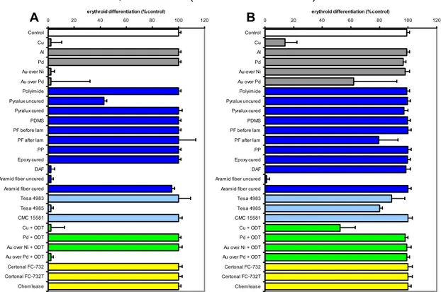
The experimental protocol for analysis of biomaterials effects on cell growth was the following: (a) cells (K562 or LCL) were cultured within biomaterial-treated 24 well plates for different days (continuous exposure); (b) cells were exposed to the different biomaterials for 1 hour, then washed and sub-cultured in standard medium conditions for different days (short-term exposure). The 1 hour short-term exposure was chosen, since this length of time is compatible with most of the protocols available in literature for cellular manipulations using Lab-on-a-chip platforms20,34,35,42-46.
In both continuous and short-term exposures, cell concentrations (cell number/ml) were determined after 3, 4, 5 and 6 days of cell growth for K562 and LCL cell lines. In Figures 3 and 4 the value determined after three days was reported; at this time, indeed, both control K562 and LCL cells are in the log-phase of cell growth, allowing the best comparison to detect cell growth inhibition in experiments aimed at studying possible inhibitors of cellular proliferation47. However similar results were obtained also at day 4, 5 and 6 (data not shown). The effects of the employed materials were considered as inhibitory effects in the case of 75% inhibition of cell proliferation, in consideration of the fact that inhibition around 50% of cell growth might be associated in K562 cells, instead to cytotoxic effects, to activation of terminal erythroid differentiation27. Results of these experiments are shown in Figures 3 and 4. In particular, in Figure 3, the data obtained, allow to conclude that continuous exposure to materials is not compatible with efficient cell growth, for the following materials: Cu, Au over Ni, Au over Pd (metals), Cu + ODT, Au over Pd + ODT (surface treatments), Pyralux uncured, DAF, aramid fiber uncured, Tesa 4985 (dielectrics/adhesives). In fact these materials inhibited cell growth of both K562 and LCL cells. Epoxy cured,
RESULTS Part I
instead, was inhibitory only on LCL cell growth. Therefore, very consistent effects were obtained on these two cellular systems when continuous exposure to the tested materials was undertaken.
When exposure was limited to 1 hour (Figure 4), most of the materials displayed no inhibitory activity, with the exception of aramid fiber uncured (which maintained the inhibitory activity on both cell lines) and DAF, Cu and Cu+ODT (which maintained the inhibitory activity only on LCL cells). Interestingly, Pyralux cured renders Pyralux compatible with cell growth (see Figures 3 and 4B). In addition, aramid fiber cured was found to be not active in inhibiting cells growth with the exception of long-time treated LCL cells. These data indicate that caution should be taken when using uncured Pyralux and aramid fibers for the construction of Lab-on-a-chip platforms.
Similar results, as shown in Figure 5, were obtained in another cell line: IB3-1. Ultimately the achieved results firmly demonstrate that some materials exhibited strong inhibitory effects on most of the cell lines and biological functions assessed. When long-term exposure was carried out uncured Pyralux, printable epoxy fully-cured, Au over Ni, Au over Pd, Au over Pd+ODT, Cu and Cu+ODT inhibited biological functions. Aluminum and palladium were found to be not cytotoxic in most of the assays employed. Preparation of the materials appears to be a critical point. In this sense, both uncured preparation of Pyralux and aramid displayed inhibitory activities in several assays, while cured Pyralux and cured epoxy films with aramid fibers did not. Ultimately with these assays has been demonstrated that most of the selected materials can be used for a short exposure of the cells, with the exception of Cu, Cu+ODT and aramid uncured.
A complete list of the tested materials and their effects on cell growth are summarized in detail in Table 2.
Part I RESULTS
Figure 3. Effects of the materials on cell proliferation of K562 and LCL cells after continuous exposure. K562 cells (A) or LCL cells (B) were cultured in RPMI, 10% FBS for different days in
24 well plates containing the indicated materials. The cell number/ml was determined and compared with control untreated cells cultured in standard conditions. The data reported in the Figure represent cell proliferation in respect to control cells (average SD from three different experiments). The cell number/ml was evaluated after 3 days, when both K562 and LCL cells are in the logarithmic phase of cell growth.
Figure 4. Effects of the materials on cell proliferation of K562 and LCL cells after short-term (1 hour) exposure. K562 cells (A) or LCL cells (B) were exposed in RPMI 10% FBS for 1 hour in 24
well plates containing the materials. After two washing steps with RPMI, cells were sub-cultured in standard conditions. The cell number/ml was determined and compared with control cells after three days of cell culture. The data represent the average SD from three different experiments.
0 20 40 60 80 100 120 140 160 Control Cu Al Pd Au over Ni Au over Pd Polyimide Pyralux uncured Pyralux cured PDMS PF before lam PF after lam PP Epoxy cured DAF Aramid fiber uncured Aramid fiber cured Tesa 4983 Tesa 4985 CMC 15581 Cu + ODT Pd + ODT Au over Ni + ODT Au over Pd + ODT Certonal FC-732 Certonal FC-732T Chemlease
cell proliferation (% control)
B 0 20 40 60 80 100 120 140 160 Control Cu Al Pd Au over Ni Au over Pd Polyimide Pyralux uncured Pyralux cured PDMS PF before lam PF after lam PP Epoxy cured DAF Aramid fiber uncured Aramid fiber cured Tesa 4983 Tesa 4985 CMC 15581 Cu + ODT Pd + ODT Au over Ni + ODT Au over Pd + ODT Certonal FC-732 Certonal FC-732T Chemlease
cell proliferation (% control)
A 0 20 40 60 80 100 120 140 160 B Control Cu Al Pd Au over Ni Au over Pd Polyimide Pyralux uncured Pyralux cured PDMS PF before lam PF after lam PP Epoxy cured DAF Aramid fiber uncured Aramid fiber cured Tesa 4983 Tesa 4985 CMC 15581 Cu + ODT Pd + ODT Au over Ni + ODT Au over Pd + ODT Certonal FC-732 Certonal FC-732T Chemlease
cell proliferation (% control)
B 0 20 40 60 80 100 120 140 160 Control Cu Al Pd Au over Ni Au over Pd Polyimide Pyralux uncured Pyralux cured PDMS PF before lam PF after lam PP Epoxy cured DAF Aramid fiber uncured Aramid fiber cured Tesa 4983 Tesa 4985 CMC 15581 Cu + ODT Pd + ODT Au over Ni + ODT Au over Pd + ODT Certonal FC-732 Certonal FC-732T Chemlease
cell proliferation (% control)
A B 0 20 40 60 80 100 120 140 160 Control Cu Al Pd Au over Ni Au over Pd Polyimide Pyralux uncured Pyralux cured PDMS PF before lam PF after lam PP Epoxy cured DAF Aramid fiber uncured Aramid fiber cured Tesa 4983 Tesa 4985 CMC 15581 Cu + ODT Pd + ODT Au over Ni + ODT Au over Pd + ODT Certonal FC-732 Certonal FC-732T Chemlease
cell proliferation (% control)
0 20 40 60 80 100 120 140 160 Control Cu Al Pd Au over Ni Au over Pd Polyimide Pyralux uncured Pyralux cured PDMS PF before lam PF after lam PP Epoxy cured DAF Aramid fiber uncured Aramid fiber cured Tesa 4983 Tesa 4985 CMC 15581 Cu + ODT Pd + ODT Au over Ni + ODT Au over Pd + ODT Certonal FC-732 Certonal FC-732T Chemlease 41-90
cell proliferation (% control)
A 0 20 40 60 80 100 120 140 160 B Control Cu Al Pd Au over Ni Au over Pd Polyimide Pyralux uncured Pyralux cured PDMS PF before lam PF after lam PP Epoxy cured DAF Aramid fiber uncured Aramid fiber cured Tesa 4983 Tesa 4985 CMC 15581 Cu + ODT Pd + ODT Au over Ni + ODT Au over Pd + ODT Certonal FC-732 Certonal FC-732T Chemlease
cell proliferation (% control)
0 20 40 60 80 100 120 140 160 Control Cu Al Pd Au over Ni Au over Pd Polyimide Pyralux uncured Pyralux cured PDMS PF before lam PF after lam PP Epoxy cured DAF Aramid fiber uncured Aramid fiber cured Tesa 4983 Tesa 4985 CMC 15581 Cu + ODT Pd + ODT Au over Ni + ODT Au over Pd + ODT Certonal FC-732 Certonal FC-732T Chemlease 41-90
cell proliferation (% control)