UNIVERSITÀ DEGLI STUDI DI CATANIA
DIPARTIMENTO DI FISICA E ASTRONOMIA
DOTTORATO IN FISICA XXIX CICLO
__________________________
Development and characterization of
nanocarbon-based devices for sensing
applications
PhD student:Salvatore Baldo
Tutors:
Prof. Giuseppe Falci (UNICT)
Dr. Silvia Scalese (CNR-IMM)
Coordinator:
Prof. Vincenzo Bellini
1.1. Introduction .……….
11.2. Graphene………...…………..
41.2.1. Introduction……….……….
41.2.2. Graphene synthesis………...
71.2.3. Graphene properties.……….…..…...
151.3. Graphene oxide……….…....
171.3.1. Introduction……….……….
171.3.2. Graphene oxide synthesis……...………...
191.3.3. Graphene oxide properties.………...
211.4. Graphene oxide reduction………...
261.5. Carbon nanotubes ………...
361.5.1. Introduction………..
361.5.2. Carbon nanotubes synthesis……….
412. Carbon-based devices
2.1. Introduction ………...
682.2. Carbon interconnects………...
702.3. Carbon nanotubes-based devices……….
732.3.1.
CNTFET and state of the art in electronics
applications………..
732.3.1.1. CNTFET in CMOS technology...
852.3.1.2.
CNTFET – TFT (Thin-Film
Transistors)………..
872.3.2.
CNT-based devices and state of the art in
sensing applications……….
912.3.2.1. CNT-based resistor………..
932.3.2.2. CNT-based SAW resonators……
952.3.2.3. CNT-based QCM devices………
972.3.2.4.
CNTFET
ChemFET……….
as
gas
sensor:
992.3.2.5.
CNT-based devices in biosensing
applications...
1042.3.2.6. CNT-based immunosensors…….
1092.4. Graphene-based devices………...
1162.4.1.
Graphene-FET and state of the art in
electronics applications………
1172.4.2.
Graphene-FET and state of the art in
sensing applications……….
121collaboration with STMicroelectronics……
3.1.4.
The issue of the parasitic capacitances in
the dielectrophoresis process………...
146
3.1.5. Repeatability of the deposition process…...
1493.2. Graphene oxide-based devices development………
1523.3.
Development of the CNT-based immunosensor for
Human Arginase-1 detection………....
154
3.3.1. Immunosensors development...
1563.3.2. Human Arginase-1 detection...
1613.3.3.
Arduino microcontroller-based system for
protein detection………...
1673.4. Graphene oxide-based sensors………...
1703.4.1.
Electrical behavior for GO and rGO based
devices in air and nitrogen environment…..
1723.4.2. AC analysis: Impedance characterization....
1763.4.3. Gas detection test: the case of the ethanol...
179Conclusions….………...
181Appendix………
183A1.
Moore's Law………..…..
183A2.
Scanning electron microscopy (SEM)……….
185A3.
Optical lithography………..
187A4.
Immunoassay in biosensing field
………
194A5.
Code developed in “C” language for the Arduino
microcontroller………
200References………..
210List of publications………
237I
nanomaterials are emerging as a powerful and general class of ultrasensitive electrical sensors for the direct detection of biological/chemical species and physical quantities.
Nanostructure science and technology is a broad and interdisciplinary area of research and development activity that has been growing explosively worldwide in the past ten years. It has the potential for revolutionizing the ways in which materials and products are created and the range and nature of functionalities that can be accessed.
Nanotechnology-based devices, due to their very peculiar properties, have advantages in high sensitivity, low energy consumption and potentially highly miniaturized integration.
Already in 1961 Feynman enunciated his famous byword “there's plenty of
room at the bottom”, which somehow let us guess the potential of
nano-science. But when is it possible to talk about “nano”? Nanostructure is a kind of structure whose size is certainly less than 100 nm while a nanostructured material contains substructures with that dimensionality.
Nanotechnologies include not just the techniques necessary to realize the nanostructures, but also all the investigation methods which allow the characterization.
II
Nanomaterials are very attractive because at nano scale unique optical, magnetic, electrical, and other properties emerge. These emergent properties have the potential for great impacts in electronics, medicine, and other fields. The Carbon nanotubes (CNTs) are a typical example of nanomaterials. They are made by graphite planes (carbon atoms arranged in a hexagonal structure) rolled up to outline a cylindrical system. A single plane of graphite is called graphene, another very interesting nanomaterials studied today in different science fields. Due to their interesting properties, currently these materials are used in various technological applications, such as the automotive area, telecommunications, aerospace industry, biomedical field and even in the production of materials for sport. Moreover, in the last decade, microelectronics industries have shown a growing interest for CNTs and graphene because they could be a possible remedy for Moore's Law (in appendix more information about this law).
Thanks to the peculiar characteristics of the nanostructures in general, such as the high surface over volume ratio, they can be used as sensitive layers in gas or biomedical sensors by exploiting the changes of their electrical characteristics induced by surface chemical modifications. In fact, the development of methods for identification of specific bio-markers is one of the major challenges in the biosensor field and CNTs are a possible way to produce very attractive sensors. For example, the detection of proteins by immunoassays usually includes methods such as ELISA (enzyme-linked immunosorbent assay) and RIA (radioimmunoassay). However, most of these techniques require sophisticated instrumentation and time-consuming procedures and most of the reagents employed in immunoassays such as antibodies, enzymes, and fluorescence labels are very expensive. Therefore, there is an increasing interest for the development of new, simple, sensitive, reliable, and cheaper diagnostic methods.
III
GO is used as a precursor to obtain graphene but, recently, it has received increasing attention in optoelectronic [5,6] and sensing [7] applications, due to its peculiar properties. GO can be viewed as a single sheet of graphene with many oxygen-containing groups, including hydroxyl, epoxy and carboxylic acid, bonded on the surface. The presence of these oxygen groups gives the possibility to tune the conductivity and enhances the hydrophilic property of GO. In particular, the hydrophilicity makes GO as an interesting material to produce humidity sensors. These last are in demand in the industrial, environmental, and structural monitoring fields. A lot of research has been conducted to fabricate high efficiency humidity sensors, based on either change in resistance [8,9] or mass [10,11], due to the presence of water molecules. In recent years, research has been conducted to achieve a high level of sensitivity and selectivity in sensors. In particular, carbon-based materials like graphene have raised great interest for the development of humidity and temperature sensors. However, pristine graphene is not useful in the sensors field, because the surface of pristine graphene is basically inert. Instead, in graphene oxide, the presence of several oxygen groups gives the possibility to making the graphene surface sensitive to the environment. Moreover, due to the oxygen groups, the electrical conductivity of GO depends also on the temperature. However, a limited amount of work has been done with regards to humidity detection using graphene and graphene
IV
oxide. Massera et al. reported using a graphene sheet as a humidity sensor, in which the graphene samples were prepared by the scotch-tape method [12]. Guo et al. used laser-reduced graphene-oxide films for humidity sensing [13], whereas a graphene oxide-silicon bilayer was used for humidity sensing by Yao et al. [14]. In these works a change in electrical resistance is reported as the mechanism for sensing humidity. Yao et al. demonstrated the sensitivity of graphene oxide to humidity by using it as a coating on quartz crystal microbalances, which is based on the concept of change in frequency due to a change in mass [15].
The subject of this PhD thesis has been the development and characterization of nanocarbon-based sensors, with particular attention to the use of easy and cheap methodologies and processes that are required for future large scale production. In the first part of the thesis the development of CNT-based devices for biosensing applications is reported and the tests on protein detection are shown. In the second part the development of GO-based devices is shown and the electrical behavior of the devices is investigated in different ambient conditions and for different oxygen functionalization (GO and reduced GO).
The thesis work is divided as follows:
In the first chapter the Carbon-like materials basics are recalled. In particular the types, the properties, and the main synthesis methods are described.
The second chapter introduces the FET/Resistor devices and then describes the most common CNTs/GO structures in literature.
V
Finally, in the conclusions the main results, work in progress, developments and future applications are discussed.
1
CHAPTER 1
Carbon Nanomaterials
1.1. Introduction
Nanotechnologies are a science branch which has as its main objective the achievement, the study and application of systems with dimensions below 100 nm. It is interesting underline that a nanometer is equivalent to 10 times the size of the hydrogen atom.
Nanomaterials can be defined as systems composed by nanometric or nanostructured units smaller than 100 nm, which are characterized by particular electrical, chemical, optical, mechanical and magnetic properties. In the case of carbon, until 1985 there were known only two forms of crystalline carbon: the diamond three-dimensional form (sp3) and the planar graphite form (sp2),called allotropic forms.
Some studies performed by the American scientist Richard E. Smalley lead to the discovery (whereby he won the Nobel award) of a third form of regular arrangement of carbon atoms (another allotropic form): the fullerenes. They are “cages” roughly spherical formed by an ordered arrangement of hexagonals and pentagonals structures of carbon atoms.
The amount of polygons and their relative proportions defines the fullerene shape and size. The first fullerene discovered was the C60 (Fig. 1.1.1), which
2
Fig. 1.1.1 - Fullerene C60 "buckyball" [wikipedia.org] (left) and the Montreal Biosphere by Buckminster Fuller [http://www.spatialagency.net/] (right)
In 1991, the Japanese researcher Sumio Iijima discovered accidentally another allotropic form among the secondary products of fullerenes: the Carbon Nanotubes (CNTs).
The latter can be seen as a single graphite plane rolled up on itself to form a tubular shape.
A carbon atom has four free electrons, which are free to bind each other. In the diamond case, four electrons are regularly coupled with the electrons of other carbon atoms, forming a tetrahedral structure (i.e. in the shape of an equilateral triangular pyramid), with a carbon at the centre and other four at the corners, with the electrons in the middle. This bond is very strong and for
3
this reason the diamond is very hard. In the graphite, however, bind stably only three electrons, and the fourth remains free. In this way, each atom is bonded to three others, to form a triangular star. Many atoms all together give rise to a planar structure formed by hexagons whose vertices are carbon atoms. This planar structure is called graphene. Therefore, graphene is a material made of a monoatomic layer of carbon atoms (i.e., having a thickness equivalent to the size of a single atom).
Another example of Carbon-like materials is the graphene oxide (GO), a single sheet of graphite oxide that can be viewed as a two-dimension network of sp2 and sp3-bonded hybridized carbon atoms arranged in a dense honeycomb crystal structure. Many oxygen-containing groups, including hydroxyl, epoxy and carboxylic acid, are bonded to the two-dimensional network.
Therefore, today we know several allotropic form of the carbon, from the most famous bulk structures such as diamond and graphite to the nanostructured ones such as fullerenes, nanotubes and graphene (Fig. 1.1.2).
4
Among various intriguing properties, its extraordinary high carrier mobility [17] makes graphene a promising material for future electronic devices. Application to conductive composite materials [18] and ultra-high sensitive sensors [19] is also expected.
Fig. 1.2.1.1 - A graphene layer [www.wikipedia.org]
As the suggestion of the ending name -ene, the atoms are hybridized in the form sp², and will therefore have to form hexagons with angles of 120° (Fig. 1.2.1.2).
5
The Nobel Prize in Physics for 2010 was awarded to Andre Geim and Konstantin Novoselov at the University of Manchester “for groundbreaking experiments regarding the two-dimensional material graphene”. In fact, in 2004, physicists at the University of Manchester and the Institute for Microelectronics Technology, Chernogolovka, Russia, first isolated individual graphene planes by using the scotch tape technique. They used adhesive tape to repeatedly split graphite crystals into increasingly thinner pieces until obtaining the graphene (see graphene synthesis paragraph). Due to its free electrons, graphene shows excellent conduction characteristics and in the last years it has become one of the most studied materials for several technological applications.
Each carbon atom in graphene is covalently bonded to other three atoms with which it shares one electron forming 𝑠𝑝2 “σ-bonds”. The fourth valence electron of a carbon atom occupies a 𝑝𝑧 orbital. The 𝑝𝑧 states mix together (π-bonds) forming delocalized electron states that are responsible for the electrical conductivity of graphene. In figure 1.2.1.2 primitive vectors of the hexagonal lattice of graphene and those of the reciprocal lattice are shown.
Fig. 1.2.1.2 - Direct lattice (a) and reciprocal lattice (b) of graphene. The grey hexagon represents the first Brillouin zone.
6
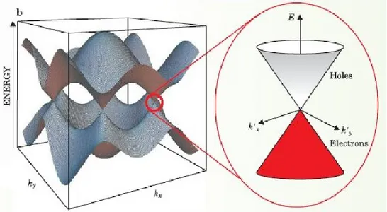
Fig. 1.2.1.3. - Valence and conduction bands of graphene. The conical shape of energy dispersion at the K-points is highlighted [M.Wilson et al., Phys. Today, 59, 2006, pp 21-23)]
Due to its particular band structure, graphene can be considered halfway between a metal and a semiconductor material, and therefore it is classified as a semi-metal or “zero-gap” semiconductor. For this reason, graphene is also used to produce transparent electrodes [20,21].
7
1.2.2. Graphene synthesis
Graphene can be produced by exfoliation of highly ordered pyrolytic graphite (HOPG), epitaxial growth, chemical vapour deposition (CVD) and the reduction of graphene oxide. The first three methods produce graphene with a relatively perfect structure and excellent properties, while in comparison, GO can be produced using inexpensive graphite as raw material by cost-effective chemical methods with high yield.
Micromechanical Exfoliation – The “Scotch Tape Method”
As already mentioned, the first reported preparation of graphene was by Novoselov and Gaim in 2004 [22] by exfoliation of graphite using a simple adhesive tape.
After peeling it off the graphite, multiple-layer graphene remains on the tape. By repeated peeling the multiple-layer graphene is cleaved into various flakes of few-layer graphene. Afterwards the tape is attached on a substrate and the glue solved, e.g. by acetone, in order to detach the tape. Finally one last peeling with an unused tape is performed (Fig. 1.2.2.1).
Fig. 1.2.2.1 – Schematization of the scotch tape method [http://www.graphene.ac.rs] (left), a real photo of the exfoliation process [https://www.sknust.de/wp-content/uploads/2014/03/graphene-exfoliation.png] (right)
8
Fig. 1.2.2.2 - Optical image of the exfoliated graphene layers on 290 nm thick oxidized silicon wafers [http://dx.doi.org/10.5772/56640]
However, it is difficult to obtain larger amounts of graphene by this method, not even taking into account the lack of controllability. The complexity of this method is basically low, nevertheless the graphene flakes need to be found on the substrate surface, which is labour intensive. The quality of the prepared graphene is very high with almost no defects and nearly ideal mechanical and electrical properties.
9
Liquid – phase exfoliation
Graphene can be prepared in liquid-phase. This allows upscaling the production, in order to obtain a much higher amount of graphene. The easiest method would be to disperse the graphite in an organic solvent with nearly the same surface energy as graphite. Thereby, the energy barrier is reduced, which has to be overcome in order to detach a graphene layer from the crystal. The solution is then sonicated in an ultrasound bath for several hours and centrifuged in order to dispose of the thicker flakes [24]. In another way, a DC voltage is applied between two electrode immersed in liquid to enhanced the exfoliation process (Electrochemical Exfoliation) [25] (Fig. 1.2.2.3).
The deposition of obtained graphene on a substrate can be performed by simple drop-casting. After the solvent evaporation, the graphene flakes remain on the surface. In order to achieve a more homogeneous coating, the sample can be rotated using the spin-coating method.
10
A totally different approach to obtaining graphene is to grow it directly on a surface. Consequently the size of the obtained layers are not dependent on the initial graphite crystal. The growth can occur in two different ways. Either the carbon already exists in the substrate (epitaxial growth) or it has to be added by chemical vapour deposition.
Epitaxial growth is a commonly used technique for creating high quality monolayer graphene. In this case, isolated monolayer of graphene is grown typically on a single-crystal of silicon carbide (SiC) by graphitization under UHV (Ultra High Vacuum) [26]. SiC is a wide-bandgap semiconductor which exists in various polytypes. For the production of epitaxial graphene, 3C- (cubic), 4H- and 6H-SiC (hexagonal) are the most commonly used polytypes. The graphitization of SiC was discovered in 1955, but it was regarded as unwelcome side effect instead of a method of preparing graphene [27].
Typically, in this growth process, under UHV annealing conditions (1200°C) the top layers of SiC crystals undergo thermal decomposition, Si atoms desorb and the carbon atoms remaining on the surface rearrange and re-bond to form epitaxial graphene layers [28-30] (Fig. 1.2.2.4.).
11
Fig. 1.2.2.4. – Epitaxial growth of graphene on SiC [Hiroki Hibino et al, Graphene growth on silicon carbide, NTT technical review, 2010] (left), TEM image of growth results [Wataru Norimatsu et al., 2014,DOI: 10.1039/C3CP54523G] (right)
The results are highly dependent on the parameters used, like temperature, heating rate, or pressure. Growth on the Si-face of hexagonal SiC wafers, under appropriate conditions exhibits manageable growth kinetics (contrary to the C-face growth) allowing better control over the number of graphene layers.
Usually, graphene is grown directly on SiC crystal but, in the last years, several modification on the epitaxy process were performed. For example, a thin Ni layer (111) can be evaporated onto a SiC crystal before of the epitaxial process. The Ni surface has a lattice structure very similar to the one of graphene, with a mismatch of the lattice constant at about 1.3% [27]. Upon heating the carbon diffuses through the Ni layer and forms a graphene or graphite layer on the surface, depending on the heating rate. The produced
12
were able to grow epitaxial graphene layers, where a very sparse graphene nucleated at high temperatures. The first graphene layer coupled strongly to the Ru substrate and the second layer was free of the substrate interaction, which had an electronic structure similar to freestanding graphene. However, several hurdles must be overcome before real applications are found.
The possibility to produce large amounts of graphene by epitaxial growth is not as good as by liquid-phase exfoliation, but the controllability of the growth and graphene size in the epitaxial technique is better. In addition, depending on the applications, graphene grown on substrate can be used in situ without transfer to another substrate. However, in order to make graphene technologically viable, the transfer of graphene films to substrates appropriate for specific applications is required. For example, using a thermal release tape, dry transfer of epitaxial graphene from the C-face of 4H-SiC onto SiO2, GaN and Al2O3 substrates was performed [32].
Growth on Surfaces - Chemical Vapour Deposition
Chemical vapour deposition (CVD) is a process in which a substrate is exposed to gaseous compounds (see appendix for more information about CVD technique). These compounds decompose on the surface in order to grow a thin film, whereas the by-products evaporate. There are different
13
ways to achieve this. Graphene can be grown by exposing of a Ni substrate to a gas mixture of H2, CH4 and Ar at about 1000°C under low vacuum [33]. The methane decomposes on the surface, so that the hydrogene evaporates. The carbon diffuses into the Ni and, after cooling down in an Ar atomosphere, a graphene layer grows on the surface (Fig. 1.2.2.5).
Fig. 1.2.2.5 - CVD graphene growth mechanism on nickel [https://www.comsol.com/paper/download/194707/alshurman_poster.pdf]
The average number of layers depends on the Ni thickness and can be controlled in this way. Furthermore, the shape of the graphene can also be controlled by patterning of the Ni layer.
Using copper instead of nickel as growing substrate results in single-layer graphene with less than 5% of few-layer graphene, which do not grow larger with time [34]. This behavior is supposed to be due to the low solubility of carbon in Cu.
CVD graphene is more likely to carry impurities due to the various materials required. However, research has shown that such impurities can be sufficiently minimized to create graphene as pure as exfoliated flakes [35].
14
polymer support, which can be attached onto the top of the graphene. After etching of the Ni or Cu, the graphene can be stamped onto the required substrate and the polymer support gets peeled off or etched away (Fig. 1.2.2.6).
Fig. 1.2.2.6 - Schematic diagram of the transfer process to an arbitrary substrate [Dissertation of Benjamin Pollard, Department of Physics, Pomona College, 2011].
Using this method several layers of graphene can be stamped onto each other in order to decrease the resistance.
15
1.2.3. Graphene properties
The following properties of graphene are extracted from a “Scientific Background on the Nobel Prize in Physics 2010 – GRAPHENE, compiled by the Class for Physics of the Royal Swedish Academy of Sciences, 5 October 2010”
Density
The unit hexagonal cell of graphene contains two carbon atoms and has an area of 0.052 nm2. We can calculate its density as being 0.77 mg/m2. A
hypothetical hammock measuring 1m2 made from graphene would thus weigh
0.77 mg.
Optical transparency
Graphene is almost transparent; it absorbs only 2.3% of the light intensity, independent of the wavelength in the optical domain. This number is given by πα, where α is the fine structure constant. Thus suspended graphene does not have any colour.
Strength
Graphene has a breaking strength of 42N/m. Steel has a breaking strength in the range of 250-1200 MPa= 0.25-1.2x10⁹ N/m2. For a hypothetical steel
film of the same thickness as graphene (which can be taken to be 3.35Å, i.e. the layer thickness in graphite), this would give a 2D breaking strength of
16
theoretically limited to μ=200,000 cm2V−1s−1 by acoustic phonons at a
carrier density of n=1012 cm−2. The 2D sheet resistivity, also called the
resistance per square, is then 31 Ω. The fictional hammock measuring 1m2
would thus have a resistance of 31 Ω.
Using the layer thickness we get a bulk conductivity of 0.96x10⁶ Ω-1cm-1 for
graphene. This is somewhat higher than the conductivity of copper which is 0.60x10⁶ Ω-1cm-1.
Thermal conductivity
The thermal conductivity of graphene is dominated by phonons and has been measured to be approximately 5000 Wm−1K−1. Copper at room temperature
has a thermal conductivity of 401 Wm−1K−1. Thus graphene conducts heat 10
17
1.3. Graphene oxide
1.3.1. Introduction
Graphite oxide has a similar layered structure to graphite, but the plane of carbon atoms in graphite oxide is heavily decorated by oxygen-containing groups, which not only expand the interlayer distance but also make the atomic-thick layers hydrophilic. As a result, these oxidized layers can be exfoliated in water under moderate ultrasonication. If the exfoliated sheets contain only one or few layers of carbon atoms like graphene, these sheets are named graphene oxide (GO). This material can be viewed as a two-dimensional network of sp2 and sp3-bonded hybridized carbon atoms arranged in a dense honeycomb crystal structure. Many oxygen-containing groups, including hydroxyl, epoxy and carboxylic acid, were bonded to the two-dimensional network. The precise chemical structure of GO is still not quite clear, which contributes to the complexity of GO due to its partial amorphous character. Several early investigations have proposed structural models of GO and the widely accepted GO model was proposed by Lerf and Klinowski (Fig. 1.3.1.1)
Fig. 1.3.1.1 – Graphene oxide structure [Mahmoud Nasrollahzadeh et al., 2015, DOI: 10.1039/C4RA12552E]
18
[37,38] and mechanical [39,40] properties of GO. It is well known that the electrical properties of GO would be influenced by some external stimulations, including reducibility reagent [41], electric field [42-44], temperature [45,46], light [47], etc. Due to the tunable electrical property, GO is considered as a potential electrical material candidate for graphene-based electronic devices.
19
1.3.2. Graphene oxide synthesis
The history of the evolution of synthesis methods and chemical structure of GO has been extensively reviewed by Dreyer et al. [48] and Compton and Nguyen [49]. The route to prepare GO involves two main steps (Fig. 1.3.2.1). Firstly, graphite powder is oxidized to produce graphite oxide, which can be readily dispersed in water or another polar solvent due to the presence of hydroxyl and epoxide groups across the basal planes of graphite oxide and carbonyl and carboxyl groups located at the edges [50–52]. Secondly, the bulk graphite oxide can be exfoliated by sonication to form colloidal suspensions of monolayer, bilayer or few-layer GO sheets in different solvents [53].
Fig. 1.3.2.1 – Synthesis of graphene oxide [Lubricants 2014, 2, 137-161, DOI:10.3390/lubricants2030137]
The critical point of preparing GO is the selection of suitable oxidizing agents to oxidize graphite. Reviewing the origin of the preparation of graphite oxide, it has had more than 150 years of history since the first report from Brodie [54] in 1859. The oxidation process was performed by adding KClO3 in a single addition to a slurry of graphite in fuming HNO3. The C/H/O ratio of the oxidation product was determined to be 2.19/1.00/0.80, which is the typical composition of graphite oxide [55]. About 40 years later, Staudenmaier [56] modified the Brodie method by using concentrated
20
Compared to the Brodie-Staudenmaier methods, the Hummers method requires less than 2 h for completion at temperatures below 45° and can be carried out safely. These three methods are the primary routes to prepare graphite oxide from graphite and have been reviewed extensively by Ruoff and co-workers [60,61]. However, all three reactions involve the liberation of toxic gas NOx and/or ClO2. Some modifications based on the Hummers method have been proposed. Kovtyukhova [62] added a pre-oxidized procedure using H2SO4, K2S2O8, and P2O5. The C/O ratio of the oxidation product was 4.0/3.1, illustrating that this was richer in oxygen than the graphite oxide prepared by the Hummers method. The method proposed by Kovtyukhova is defined as a typical modified Hummers method and has been cited by many researchers in recent years [63–65].
21
1.3.3. Graphene oxide properties
Electrical properties
The properties of GO are different than pristine graphene due to the presence of the oxygen-containing groups. In particular, the quantity, the type of these groups and the environment play an important role in the electrical conductivity.
Intrinsic properties, such as the oxygen sites in GO and the dependence between conductivity (ϭ) and oxygen concentration have been investigated [66–77]. Several conduction mechanisms, such as Mott variable range hopping (VRH) [70–73], Efros–Shklovskii (ES) VRH (the modified VRH model that considers the Coulomb gap) [74], Arrhenius behavior [75,76], and fluctuation-induced tunneling (FIT) [77] conduction have been suggested. Kazuto Hatakeyama et al. studied the GO conduction finding that, in GO with high amount of functional groups, the electrical transport is basically an H+ proton transport. They show that, in air environment, the conductivities (σ) of multilayer graphene oxide films (assembled by the drop-cast method) are larger than those of single-layer GO (prepared in the same way). In particular, at 60 % relative humidity (RH), the σ value increases from 1x10⁻⁶ S cm-1 in single-layer GO to 1x10⁻⁴ and 4 x10⁻⁴ S cm-1 for 60 and 200 nm thick multilayer films, respectively [78]. As described by Anderson's proton conductivity model [79], at a low RH, only a small amount of water molecules is adsorbed onto the surface active hydrophilic groups (i.e., hydroxyl) of GO sheets through hydrogen bonding, and hence, the GO surface is not completely water-covered. With the increasing adsorption of water molecules, hopping proton mechanism plays an important role. Protons
22
Fig. 1.3.3.1 – The electrical interaction mechanism between GO films and water molecules [80]
A proposed mechanism for proton conductivity in GO is shown in Fig. 1.3.3.2. In multilayer GO, mobilized protons can change path from one layer to the surrounding layers through nanopores, which results in increased conductivity. Proton mobility and hydrogen bond reformation in single and multilayer GO films is supported by single and double GO walls, respectively [78].
P t
23
Fig. 1.3.3.2 – Proposed mechanism for proton conductivity. a) In multilayer GO, protons can change from the conduction path in one layer to another through nanopores. The sp3 - and sp2 -hybridized areas are denoted in dark grey and light grey, respectively. Proton transfer supported by single (b) and double (c) GO walls, respectively [78].
As GO bears various hydrophilic functional groups, it is necessary to identify the main factors that influence proton conductivity in GO. It was observed strong electrostatic attractions between the negatively charged epoxy groups of GO and transition metal ions [81].
Based on this observation, Kazuto Hatakeyama et al. described how the epoxy sites could be successfully blocked with ethylenediamine, obtaining a functionalized GO also called enGO. A decrease in the enGO conductivity was observed confirmed that the epoxy sites act as the major vehicle for proton transport in GO [78].
24
semiconducting behaviour [82]. These results showed that in the case of GO with lower amount of functional groups (typical case of reduced GO, see below) the electrical transport is not a proton transport.
AC analysis – Impedance Spectroscopy
An evaluation of the electrical transport properties in AC voltage could provide useful information about the material. A typical electrical characterization in AC is the impedance spectroscopy. In this technique the impedance of the material is measured over a range of frequencies typically from 20Hz to 1MHz using an LCR meter. The results are shown in a Nyquist plot, where the imaginary part of the impedance is in the y axis and the real part is in the x axis. Yao et al. found that GO exhibit two types of impedance: semicircle-type impedance and straight line-type impedance.
The semicircle-type impedance is associated with the bulk impedance of GO films, and it can be electrically equivalent to a parallel circuit of a resistor RGO and a capacitor CGO, as shown in Fig. 1.3.3.3., where RGO and CGO represent the bulk resistor and geometric capacitance of the GO films, respectively. Instead, the straight line-type impedance is due to the Warburg impedance, caused by the diffusion of ions across the interface between the GO films and the electrodes. Warburg impedance can be modelled as
25
additional impedance Zw, as shown in Fig. 1.3.3.3. [80]. Typically, the straight line-type impedance is present in GO with high amount of oxygen-containing groups (in which is present a proton transport) while the semicircle-type impedance is present in GO with low quantities of oxygen-containing groups.
Fig. 1.3.3.3. – Impedance analysis of GO film in the case of semicircle-type impedance (up) and in the case of straight line-type impedance (down) [80]
26
graphene. However, reduction approach produces disordered graphene-like materials and not all sp3 carbon atoms are converted to sp2. This is mainly because the decomposition of oxygen-containing groups also removes carbon atoms from the carbon plane, which splits the graphene sheets into small pieces and results in the distortion of the carbon plane. Defects inevitably affect the electronic properties of the material by decreasing the transport path and introducing scattering centres. Therefore, rGO has much lower mobility than the exfoliated graphene, mainly because plenty of defect remain in rGO. The conductivity of monolayer graphene mainly relies on carrier transport within the carbon plane, as a result, functional groups attached to the plane are the main influencing factor on its conductivity, while functional groups attached to the edge have less influence. Consequently, the reduction of GO can be obtained removing epoxy and hydroxyl groups on the plane, while other groups, e.g. carboxyl, carbonyl and ester groups, present at the edges or defective areas only have a limited influence on the conductivity of an rGO sheet.
There are many approaches available to achieve reduction of GO, such as thermal, chemical and optical method.
27
Thermal annealing
GO can be reduced to graphene-like sheets by heat treatment and the process is named thermal annealing reduction. There are several ways to obtain a heating, for example through a furnace, a hot plate or also by optical or electromagnetic irradiation.
The heating temperature significantly affects the reduction on GO.
Schniepp et al. [83] found that if the temperature was less than 500 °C, the C/O ratio was no more than 7, while if the temperature reached 750 °C, the C/O ratio could be higher than 13.
Wang et al. [84] annealed GO thin films at different temperatures, showed that the electrical conductivity of the reduced GO film obtained at 500 °C was only 50 S/cm, while at 700 °C and 1100 °C it could be 100 S/cm and 550 S/cm, respectively (Fig. 1.4.1).
Fig. 1.4.1. - Increase of the average conductivity of graphene films from 49, 93, 383 to 550 S/cm, along with the temperature increasing from 550 °C, 700 °C, 900 °C to 1100 °C, respectively [84].
28
recovery of GO, otherwise the films can be quickly lost through reaction with residual oxygen in the system. The same consideration can be done in inert atmospheres.
For the third case, a reducing gas such as H2 is added to consume the residual oxygen in the atmosphere. Moreover, because of the high reducing ability of hydrogen at elevated temperatures, the reduction of GO can be performed at low temperature in a H2 atmosphere. For example, Wu et al. reported that GO can be reduced at 450 °C for 2 h in an Ar/H2 (1:1) mixture with a resulting C/O ratio of 14.9 and conductivity of ~1 · 103 S/cm.
Based on the above results, in general the reduction of GO by high temperature annealing is desired but, high temperature means large energy consumption and critical treatment conditions. For example, some applications need to have GO on substrates, but high reduction temperature cannot be used for GO films on substrates with a low melting-point, such as glass or plastic.
The binding energy between graphene and different oxygen-containing functional groups can be an important index to evaluate the reducibility of each group attached to the carbon sheet. Using density functional theory (DFT) calculation, Kim et al. [89] obtained the binding energy of an epoxy group (62 kcal/mol) and a hydroxyl group (15.4 kcal/mol) to a 32-carbon- atom graphene unit, which indicates that epoxy groups are much more stable
29
than hydroxyl groups in GO. In a calculation by Gao et al. [90] (Fig. 1.4.2.), the epoxy and hydroxyl groups in GO are divided into two types for their different locations at the interior of an aromatic domain of GO (A, B) and at the edge of an aromatic domain (A’, B’).
Fig. 1.4.2 – Schematic of oxygen-containing groups in GO: A, epoxy groups located at the interior of an aromatic domain of GO; A’, epoxy groups located at the edge of an aromatic domain; B, hydroxyl located at the interior of an aromatic domain; B’, hydroxyl at the edge of an aromatic domain; C, carbonyl at the edge of an aromatic domain; and D, carboxyl at the edge of an aromatic domain [90].
Due to the low binding energy, a single hydroxyl group attached to the interior aromatic domain is not stable and is subject to dissociation at room temperature, while a hydroxyl group attached to the edge is stable at room temperature. As a result, hydroxyl groups attached to the inner aromatic domains of GO are expected to dissociate or migrate to the edges of aromatic domains.
Jeong et al. [92] has investigated the thermal stability of graphite oxide. According to their results, most of the oxygen- containing groups can be removed by annealing at 200 °C in low-pressure argon (550 mTorr). After annealing for 6 h, according to the results of Fourier-transformed infrared
30
rather difficult even at temperatures as high as 1200 °C.
Microwave and photo reduction
There are several alternative to perform thermal reduction, including microwave irradiation (MWI) [93,94] and photo-irradiation [95,96]. The main advantage of MWI over conventional heating methods is heating substances uniformly and rapidly. By treating graphite oxide powders in a commercial microwave oven, rGO can be readily obtained within 1min in ambient conditions [93].
Flash reduction [95] of GO films can be performed with a single flash from a xenon lamp. The photo energy emitted by the flash lamp at a close distance (<2mm: ~1 J/cm2) can provide 9 times the thermal energy needed for heating GO (thickness ~1 µm) over 100°C, which should be more than enough to induce deoxygenating reactions, and suggests that flash irradiation could lead to a much higher degree of reduction of GO. The GO films typically expand tens of times after flash reduction because of rapid degassing, and the electrical conductivity of the expanded film is around 10 S/cm using its maximum expanded thickness in the calculation. Because the light can be easily shielded, rGO patterns can be easily fabricated with photomasks,
31
which facilitates the direct fabrication of electronic devices based on rGO films, as shown in Fig. 1.4.3.a.
A further improvement of the photo-reduction and patterned film fabrication was carried out with femtosecond laser irradiation as proposed by Zhang et al. [96]. The focused laser beam (laser pulse of 790 nm central wavelength, 120 fs pulse width, 80 MHz repetition rate, focused by a 100x objective lens) has even higher power density than a xenon lamp flash and the heated area in a GO film is very localized with a line width in the range of 10-1–10 µm. As a result, the laser reduction can produce rGO films with a much higher conductivity of 256 S/cm, and the rGO film patterns can be drawn directly by a pre-programmed laser on the GO film to form more complicated and delicate circuits as shown in Fig. 1.4.3. b,c,d,e.
Fig. 1.4.3. – Patterned rGO film obtained by (a) flash reduction [95] and (b-e) femtosecond laser reduction [96]. The black parts in the films are the reduced GO patterns.
The reduction of GO by visible laser irradiation depends on many experimental parameters. Maria A Buccheri et al. show that the laser irradiation of GO samples mainly caused a variation in the type of oxygen functional groups and a decreasing of GO planes dimension respect to the
32
in the Raman spectra. In agreement with the Raman results, XPS analysis shows that the irradiation reduces the sp2 component while the signals related to the oxygen configurations that are stable on defects (C=O, COOH and C– OH) increase, suggesting the creation of more holes or edges. DLS analysis on irradiated and initial samples confirmed that the average size of the irradiated samples is about half the value of initial GO, confirming a reduction in the size after laser irradiation. The SEM image of the irradiated sample shows a series of much smaller objects, with irregular edges. Summarizing, the pulsed visible laser irradiation of the GO solution in water produces more defects in the GO structures with the creation of a population of GO flakes with reduced dimensions and irregular shape. These results are different from other literature data [98] that report the reduction of the oxygen content in GO flakes irradiated by pulsed visible laser. The main differences are the GO concentration and the irradiated volume of GO as well as the frequency and energy of the pulsed laser, suggesting a dependence on these parameters for the modification of the content and type of oxygen functionalities of GO.
33
Chemical reduction
Reduction by chemical reagents is based on their chemical reactions with GO. Usually, the reduction can be performed at room temperature or by moderate heating. As a result, the requirement for equipment and environment is not as critical as that of thermal annealing treatment, which makes chemical reduction a cheaper and easily available way for the mass production of graphene compared with thermal reduction.
The reduction of graphite oxide by hydrazine was used before the discovery of graphene [99], while the use of hydrazine to prepare chemically derived graphene was first reported by Stankovich et al. [100,101]. These reports an easy way for the mass-production of graphene. The reduction by hydrazine and its derivatives, e.g. hydrazine hydrate and dimethylhydrazine [102], can be achieved by adding the liquid reagents to a GO aqueous dispersion, which results in agglomerated graphene-based nanosheets due to the increase of hydrophobility. When dried, an electrically conductive black powder with C/O ratio around 10 [101] can be obtained. The highest conductivity of rGO films produced solely by hydrazine reduction is 99.6 S/cm combined with a C/O ratio of around 12.5 [103].
In another way, GO can be reduced keeping it in colloidal state in water by adding soluble polymers [100] as surfactant, in order to change the charge state of rGO sheets. The graphene sheets suspended in colloidal solutions can be used to assemble macroscopic structures by simple solution processes like filtration [104].
Metal hydrides, such as sodium borohydride (NaBH4) has been also used as strong reducing reagents, resulting more effective than hydrazine as a reductant of GO [105]. However, NaBH4 reacts with water, which is the main solvent for the exfoliation and dispersion of GO. In alternative way, Ascorbic
34
(HI), for GO. The investigations report C/O ratio around 15 and the conductivity of the rGO films around 300 S/cm, both better than obtained by other chemical reduction methods. The reduction by HI can be perdormed using GO in colloid form, powder or film in a gas or solution environment, even at room temperature [107].
Photocatalyst reduction
GO can be reduced also by photo-chemical reactions with the assistance of a photocatalyst like TiO2. Recently, Williams et al. reported the reduction of GO in a colloid state with the assistance of TiO2 particles under ultraviolet (UV) irradiation. As shown in Fig. 1.4.4, a change in color from light brown to dark brown can be seen as the reduction of GO proceeds [108]. This color change suggested as partial restoration of the conjugated network in the carbon plane like that in chemical reduction processes. According to the formula shown in Fig. 1.4.4, upon UV-irradiation, charge separation occurs on the surface of TiO2 particles. In the presence of ethanol the holes produce ethoxy radicals, thus leaving the electrons to accumulate within the TiO2 particles. The accumulated electrons interact with GO sheets to reduce functional groups.
35
Fig. 1.4.4 – Color change of a 10mM solution of TiO2 nanoparticles with 0.5 mg/mL GO before and after UV irradiation for 2 h in ethanol. A suspension of 10 mM TiO2 nanoparticles is also shown for comparison [108].
Electrochemical reduction
Another method for the GO reduction is based on the electrochemical removal of oxygen functionalities [109–112]. Electrochemical reduction of GO sheets can be carried out in a normal electrochemical cell using an aqueous buffer solution at room temperature. The reduction is due to the electron exchange between GO and electrodes. In particular, after depositing GO on a substrate, an electrode is placed opposite the GO film in an electrochemical cell and reducing occurs during charging of the cell.
Zhou et al. [109] reported the best reduction effect using an electrochemical method. Elemental analysis of the resultant rGO revealed a C/O ratio of 23.9, and the conductivity of the rGO film produced was measured to be approximately 85 S/cm. They found also that the reduction can be controlled by the pH of the buffer solution.
Finally, An et al. [111] used electrophoretic deposition (EPD) to make GO films. They found that GO sheets can be reduced also on the anode surface during EPD.
36
CNTs can be divided in two large families: single-walled CNTs, or SWCNT and multi-walled CNTs, or MWCNT.
The SWCNT can be regarded, for conformation and structure, belonging to the fullerene family, while MWCNTs to the nanowires family, which represent a particular case.
SWCNT
The first SWCNTs were produced in 1993 through an arc discharge system (which we will discuss later) with electrodes composed by a coal-cobalt mixture.
An ideal SWCNT can be described as a carbon tube formed by a layer of graphene rolled up on itself to form a cylinder, closed at both ends by two hemispherical caps (Fig. 1.5.1.1 a). The nanotubes body is formed just by hexagons, while the closing structures (its hemispheres) are formed by hexagons and pentagons, as regular fullerenes. For this reason the SWCNT can be considered as a sort of “giant fullerenes”, and for this reason are also called “buckytubes”.
37
In the reality, the CNTs have got often structural defects or imperfections in the geometric structure (e.g. the presence of pentagonal or heptagonal defects on the tube walls) which deform the cylinder.
Fig. 1.5.1.1 – (a) An Ideal SWCNT closed by two semi-fullerenes [http://www.phys.ttu.edu/], (b) SWCNT TEM image [Iijima et al.,1993, doi:10.1038/363603a0]
The SWCNT diameter is included between a minimum of 0.7 nm (consistent to twice of the graphite interplanar distance) and a maximum of 10 nm, but in most cases, the diameter is less than 2 nm.
The high ratio (104 - 105) between length and diameter of the SWCNT allows to consider them virtually as one-dimensional nanostructures, and gives to these molecules some specifics properties, which we will see later.
The graphene sheet "rolled up" can be described by a “chiral vector” C (or helicity), which connects two crystallographically equivalent sites and it is
38 SWCNT Armchair;
0°<θ<30° if n≠m≠0, then I have a SWCNT Chiral.
Fig. 1.5.1.3 – SWCNT schematic models: CNT “armchair” (5,5) (high), CNT “zigzag” (9,0) (center), CNT chirale (10,5) (down) [http://ipn2.epfl.ch]
The angle changes according to the law:
𝜃 = 𝑎𝑟𝑐𝑡𝑎𝑛 [
√3𝑚
2𝑛 + 𝑚
]
Fig. 1.5.1.2 – Chiral vector representation [http://ykkato.t.utokyo.ac.jp/nanotubechiral
39
The diameter d is proportional to n and m according to the law:
𝑑 =
𝑎
𝜋
√𝑚
2+ 𝑛
2+ 𝑚𝑛
where ais the graphite lattice constant (a = 0.25 nm).
Therefore we can conclude that the geometrical properties of SWCNT are completely determined by the chiral vector (i.e. from the numbers n and m).
MWCNT
Multi-wall carbon nanotubes (MWCNTs) are formed by several coaxial SWCNTs, and the distance between two neighbor walls is equal to the distance between two graphitic planes in graphite. Their outer diameter usually ranges between 10 and 20 nm, depending on the number of walls. Each “tube” contained in a MWCNT can have different diameter and chirality and therefore different properties, and most importantly interacts with the adjacent tubes (Fig. 1.5.1.4). The border between a multi-walled nanotube and a nanowire is not well defined, and a large size MWCNT can be considered as a specific case of tubular fiber.
The MWCNTs often present a large number of structural imperfections, and show an extreme variety of configuration in their terminal zones.
40
(a) (b)
Fig. 1.5.1.4 - (a) different types of MWCNT [www.maranza.com], (b) TEM images of double-wall CNT (DWCNT) and a MWCNT [www.intechopen.com]
41
1.5.2. Carbon nanotubes synthesis
One of the CNTs synthesis techniques is the arc discharge technique which allowed Iijima to observe for the first time the CNTs. The Japanese scientist observed tubular fullerenic structures by using a transmission electron microscope (TEM) in the soot produced in an arc discharge between two graphite electrodes. Since 1991, the CNTs discovery year, several other synthesis techniques were introduced, such as laser ablation and chemical vapor deposition (CVD).
Along with the CNTs other species can form in a synthesis process, from catalytic metal particles to amorphous carbon and non-tubular fullerenes, which require a later purification.
CNTs by Arc Discharge
The schematic diagram of the arc discharge system is shown in figure 1.5.2.1. Two graphite rods are used as electrodes within a vacuum chamber in the presence of inert gas.
When the pressure inside the chamber is stabilized, a voltage is applied between the graphite rods and the two rods are approached until the discharge turns on. In order to maintain the discharge on, the positive electrode is gradually approached to the negative one such a way that the gap between the anode and cathode is constant, while the anode is consuming. The energy is sufficient to vaporize the anode and a plasma is formed between the electrodes. The temperature in the plasma region can reach thousands degrees and C atoms and small agglomerates, called cluster, condense in CNT and other structures, depositing on the negative electrode and on the chamber walls.
42
Fig. 1.5.2.1 – Schematic diagram of Arc discharge
[http://lem.ch.unito.it/didattica/infochimica/2006_Nanotubi/frame-sintesi.html]
The two most important parameters in the arc discharge synthesis are the arc current control and the inert gas pressure, which determine the deposition speed.
The growth temperatures are higher than all other CNTs synthesis methods, which guarantees the best crystallinity and perfection of the tubes. Moreover, this technique allows a high CNT production yield, but it has poor process control, and it does not permits the direct the growth on substrates.
If both electrodes are produced in graphite, the main arc discharge products are MWCNTs. The catalytic particles absence avoids purification processes using heavy acid, so the MWCNT are free of defects.
To obtain SWCNT, the electrodes are doped with a small amount of catalytic metal particles which thus, are found in the deposited material together with other impurities.
Using a gaseous mixture of methane at 10 torr and argon at 40 torr, a current of 200A and a voltage of 20V, Iijima and Ichihashi have synthesized for the
43
first time SWCNTs, with diameter of about 1 nm [113]. Subsequently using carbon electrodes and catalytic particles of Co, Ni, and Fe, with a current of 95-105A and helium at 100-500 torr, SWCNT with diameter of about 1.2 nm have been synthesized by using catalytic particles of Co [114]. The quantity and quality of the nanotubes obtained depends on various parameters, such as the metal concentration, the gas type, the discharge current and the geometry of the system.
The catalytic metal particles concentration affects the CNTs quality, because the presence of these particles in the reaction product requires a purification process which alter the tubes structure.
The high particles concentration, especially if these are Co and Mo, also affects the tubes diameter, which is reduced between 0.6 and 1.2 nm [115]. The inert gas choice allows to control lightly the SWCNT diameter because the thermal conductivity and the gas diffusion coefficient affect the carbon atoms and metal condensation near to the cathode.
For example, it has been observed that the CNTs diameter decreases about 0.2 nm if the argon-helium ratio increases of the 10%, compared to the only argon presence which contributes to the SWCNT formation with a diameter of 1.2 nm [116].
Over the years various type of arc discharge techniques have been introduced allowing to obtain MWCNTs with a high purity degree, low cost and in large scale.
The arc discharge in liquid nitrogen (LN2 Arc discharge) (Fig. 1.5.2.2),
for example, allows to synthesize MWCNT highly crystalline with the possibility of mass production without the necessity to use inert gas and vacuum systems.
44
Fig. 1.5.2.2 - Arc discharge in liquid nitrogen
CNTs by Chemical Vapor Deposition (CVD)
The CNTs large scale production is often more convenient with Chemical Vapor Deposition (CVD) technique. The CNTs are formed by the hydrocarbon decomposition at the vapor state in the catalyst presence, using an energy source which is typically an electron beam, a plasma or a resistive coil heated for Joule effect. It is a continuous process in which the carbon source is continuously replaced by the flowing gas.
The energy source shatters the molecules in reactive radical species, at temperatures between 500 and 1200 °C. The reactive species diffuse to a substrate, heated and covered with catalyst particles, to which remain linked forming carbon nanotubes. The technique was used in 1959 for the production of fibers and filaments of carbon, and after CNTs discovery by
45
Iijima, it was used for the CNTs synthesis using benzene, acetylene, ethylene, methane as hydrocarbons, and nanoparticles of Ni, Fe, Co and Mo as catalysts. The catalytic particles size and type, the hydrocarbon used and the temperature, are the main parameters of the CNTs growth.
The experiments show that the MWCNT growth is favored by most of the hydrocarbons used, at temperatures between 600 and 900 °C, while the SWCNT formation requires the use of stable hydrocarbons (including CO and CH4) at temperatures between 900 and 1200 °C, presumably because their diameter is smaller and leads to a greater curvature and formation energy. Increasing temperatures also increase the CNTs density and the growth speed.
The catalytic particles are generally of Fe, Ni or Co or organometallic solids as ferracene, cobaltocene and nichelocene. Their sizes are found to affect the CNTs diameter. Compared to the arc discharge, the growth on substrates is possible, but for both MWCNTs and SWCNTs catalytic particles are required. Moreover, because of the chemical process nature and low temperatures (compared to the arc discharge), the CNTs grow with many defects.
CNTs Growth mechanism in CVD synthesis
The CNT growth mechanism is still not very clear and in the literature there are many different opinions.
In general, the catalyst-based growth process (as the CVD) can be of two types: root growth and tip growth.
46
Fig. 1.5.2.3 - CNT root growth [http://students.chem.tue.nl]
Tip growth
In this case, the carbon gas is deposited on the catalyst forming a solid solution. After solution saturation, the carbon precipitates on the catalyst surface, binds to the substrate and begins to grow in a tubular shape, dragging up the catalyst.
Fig. 1.5.2.4 - CNT tip growth [http://students.chem.tue.nl]
47
Fig. 1.5.2.5 – A TEM image were a MWCNT with a catalytic particle inside is shown [Ivanov V., et al., 33, 1727-1738 (1995)].
CNTs by Plasma Enhancement CVD (PE-CVD)
The CNTs synthesis with CVD stimulated by plasma (Plasma Enhancement CVD) consists in glow discharge producing inside a chamber or into a reaction furnace, through a high-frequency alternate voltage applied between two electrodes (Fig. 1.5.2.6).
The CNT growth happens through the glow discharge (caused by high-frequency generator) on the nanometric catalytic particles (prepared by the catalyst sputtering on the substrate).
48
CNTs by Thermal CVD
In this case, a metal catalyst (Fe, Ni, Co, or their alloy) is deposited on a substrate and subsequently etched in a HF solution (in distilled water) in order to obtain a discontinuous layer. Then it is inserted into a quartz tube inside a furnace. Heating the metal film catalyst at a temperature between 750 and 1050 °C, there is the formation on the substrate of nanometric catalytic particles on which occurs the MWCNT growth.
Using Fe as a catalyst, the CNTs diameter depends on the film thickness, and it changes between 30 and 40 nm or between 100 and 200 nm, respectively, for a thickness of 13 nm and 27 nm [119].
CNTs by Laser Ablation
The laser ablation technique (or laser vaporization technique) for the CNTs synthesis was used for the first time in 1996 by Smalley et al. [120]. Etching a carbon target with intense laser pulses, mass spectroscopy put previously in evidence the fullerenes presence.
Smalley's group was able to produce large quantities of fullerenes C60 only in a high temperature furnace, leading subsequently to the SWCNT
49
production. In figure 1.5.2.7. a schematics of a laser ablation system is reported.
A laser beam, usually a YAG or a CO2 laser, is introduced through a window inside a quartz tube, and focused towards a graphite target (eventually doped with Co, Ni, Fe or Y catalytic particles) located in the tube at the center of the furnace. The target is vaporized in the presence of an inert gas at high temperature (500-1200 °C). Pressure and gas flow are kept constant by a control system, typically at 1cm/s and 500 torr.
The CNTs produced during the graphite vaporization, together with the catalytic particles and other impurities, are conveyed and collected on a water cooled trap, while the vaporization surface is kept as cool as possible moving the laser focus or moving the target.
Fig. 1.5.2.7 – A laser ablation system diagram [http://students.chem.tue.nl]
When the graphite steam cools, the molecules and the carbon atoms condense quickly forming clusters containing fullerenes. The catalytic particles condense less rapidly and attack the cluster impeding their closure in closed structures and opening even those which are already formed. From these
50
catalytic particles nature and the gas flow in the tube. The laser ablation is an expensive technique, which makes it rarely used especially in the MWCNT synthesis.
CNTs Purification
It is predicted theoretically and observed experimentally that CNTs possess excellent physical and chemical properties and have wide-range potential applications. However, only some of these properties and applications have been verified. To a great extent, this situation can be ascribed to the difficulties in getting high-purity CNTs. Because as-prepared CNTs are usually accompanied by carbonaceous or metallic impurities, purification is an essential issue to be addressed.
Considerable progress in the purification of CNTs has been made and a number of purification methods including chemical oxidation, physical separation, and combinations of chemical and physical techniques have been developed for obtaining CNTs with desired purity.
Carbonaceous impurities typically include amorphous carbon, fullerenes, and carbon nanoparticles (CNPs) (as shown in Fig. 1.5.2.8). Because the carbon source in arc discharge and laser ablation comes from the vaporization of graphite rods, some un-vaporized graphitic particles that have fallen from the
51
graphite rods often exist as impurity in the final product. In addition, graphitic polyhedrons with enclosed metal particles also coexist with CNTs synthesized by arc discharge and laser ablation as well as high temperature (>1000 °C) CVD. Fullerenes can be easily removed owing to their solubility in certain organic solvents. Amorphous carbon is also relatively easy to eliminate because of its high density of defects, which allows it to be oxidized under gentle conditions. The most knotty problem is how to remove polyhedral carbons and graphitic particles that have a similar oxidation rate to CNTs, especially SWCNT.
Metal impurities are usually residues from the transition metal catalysts. These metal particles are sometimes encapsulated by carbon layers (varying from disordered carbon layers to graphitic shells, as shown in Fig. 1.5.2.8 b and c making them impervious and unable to dissolve in acids.
Another problem that needs to be overcome is that carbonaceous and metal impurities have very wide particle size distributions and different amounts of defects or curvature depending on synthesis conditions, which makes it rather difficult to develop a unified purification method to obtain reproducibly high-purity CNT materials.
Fig. 1.5.2.8 - TEM images of (a) amorphous carbon and fullerene molecules on the surface of CNTs, (b) metal nanoparticles covered by amorphous carbon layer, (c) metal nanoparticles covered by graphitic carbon multi-layer [Fang HT et al., Chem Mater 2004;16(26):5744–50]
![Fig. 1.2.2.2 - Optical image of the exfoliated graphene layers on 290 nm thick oxidized silicon wafers [http://dx.doi.org/10.5772/56640]](https://thumb-eu.123doks.com/thumbv2/123dokorg/4480618.32316/18.774.117.662.323.606/optical-image-exfoliated-graphene-layers-oxidized-silicon-wafers.webp)
![Fig. 1.2.2.6 - Schematic diagram of the transfer process to an arbitrary substrate [Dissertation of Benjamin Pollard, Department of Physics, Pomona College, 2011]](https://thumb-eu.123doks.com/thumbv2/123dokorg/4480618.32316/24.774.124.649.465.685/schematic-transfer-arbitrary-substrate-dissertation-benjamin-pollard-department.webp)
![Fig. 1.3.3.1 – The electrical interaction mechanism between GO films and water molecules [80]](https://thumb-eu.123doks.com/thumbv2/123dokorg/4480618.32316/32.774.181.592.355.633/fig-electrical-interaction-mechanism-films-water-molecules.webp)
![Fig. 1.3.3.3. – Impedance analysis of GO film in the case of semicircle-type impedance (up) and in the case of straight line-type impedance (down) [80]](https://thumb-eu.123doks.com/thumbv2/123dokorg/4480618.32316/35.774.117.639.277.547/fig-impedance-analysis-film-semicircle-impedance-straight-impedance.webp)
![Fig. 1.4.1. - Increase of the average conductivity of graphene films from 49, 93, 383 to 550 S/cm, along with the temperature increasing from 550 °C, 700 °C, 900 °C to 1100 °C, respectively [84]](https://thumb-eu.123doks.com/thumbv2/123dokorg/4480618.32316/37.774.202.573.569.844/increase-average-conductivity-graphene-films-temperature-increasing-respectively.webp)
![Fig. 1.4.3. – Patterned rGO film obtained by (a) flash reduction [95] and (b-e) femtosecond laser reduction [96]](https://thumb-eu.123doks.com/thumbv2/123dokorg/4480618.32316/41.774.112.672.512.788/fig-patterned-obtained-flash-reduction-femtosecond-laser-reduction.webp)

![Fig. 2.3.2.5.1 – a) Typical design of an enzyme-based electrochemical biosensor. b) SWCNT electrically-contacted glucose oxidase electrode [Carmen-Mihaela Tîlmaciu 2015, doi: 10.3389/fchem.2015.00059]](https://thumb-eu.123doks.com/thumbv2/123dokorg/4480618.32316/117.774.146.641.479.683/typical-electrochemical-biosensor-electrically-contacted-electrode-mihaela-tîlmaciu.webp)
![Fig. 2.3.2.5.2 - Schematic illustration of an amperometric biosensor for PSA detection [Carmen-Mihaela Tîlmaciu 2015, doi: 10.3389/fchem.2015.00059]](https://thumb-eu.123doks.com/thumbv2/123dokorg/4480618.32316/118.774.169.604.179.512/schematic-illustration-amperometric-biosensor-detection-carmen-mihaela-tîlmaciu.webp)
