Faculty of Sciences
PhD in Chemistry
Modeling transport
properties of molecular
devices by a novel
computational approach
Candidate
Supervisors
Michele Visciarelli
Prof. Vincenzo Barone
Prof. Ivo Cacelli
Dott. Alessandro Ferretti
Contents
1 Introduction 1
2 Molecular Electronics 7
2.1 Molecular requirements for electronic conduction . . 12
2.2 Computational strategies for molecular devices . . . 14
3 Electron Transport in Nanostructures 21 3.1 Landauer-B¨uttiker model . . . 24
3.2 Transmission function evaluation . . . 29
3.3 Implementation of the method: the FOXY code . . . 38
3.3.1 Implementation in the Gaussian package . . . 45
4 Application of the method to molecules of interest 51 4.1 Calibration of the method . . . 53
4.2 Molecular Rectifiers . . . 57
4.3 Binuclear transition metal complexes . . . 69
4.4 Diarylethene-based molecular switch . . . 81
5 Conclusions 89 5.1 Future perspectives . . . 92
Appendices 97
iii
A Green’s Function 99
B Lippman-Schwinger Equation 103
Chapter 1
Introduction
It might be just a drop in the ocean, but tomorrow it could flavour someone’s salad.
Caterina Buscaglione Gordon Moore, in 1965, predicted that the number of transis-tors per square centimetre of Silicon should have doubled every 18 months. Such prediction has been proved accurate until now, and it has become a sort of a “law” in integrated circuit miniaturiza-tion (the famous Moore’s Law1), with academical and industrial efforts directed in making the “law” valid as long as possible. This requires that the size of transistors and the interconnecting wires between them decrease at the same rate, which, until now, has been possible with the introduction of more and more precise photolito-graphic techniques (capable of defining smaller and smaller patterns in which fabricate Silicon transistors, with dimensions in the or-der of tens of nanometers each), and the use of innovative materials both for the devices themselves and for the interconnections (such as high-K dielectrics for the transistors or Copper for the
2 tions). However, in the near future, the fundamental limits rooted in the technology currently used to build transistors (Complemen-tary Metal-Oxide-Semiconductor technology, or CMOS technology) will be reached, and new technological solution should be sought in order to try to maintain the validity of the Moore’s Law as long as possible. For 50 years, the idea of using fundamental nanoscale component to build computers has been investigated. The first hint in the future direction of nanoscale science for electronics was given by Richard Feynman in his 1959 lecture entitled “There’s plenty of room at the bottom”,2 which is considered by some people as one of the “starting point” in the field of nanotechnology:
I dont know how to do this on a small scale in a practical way, but I do know that computing machines are very large, they fill rooms. Why can’t we make them very small, make them of little wires, little elements and by little I mean little. For instance, the wires should be 10 or 100 atoms in diameter, and the circuits should be a few thousand angstroms across. [...] There is plenty of room to make them smaller. There is nothing that I can see in the laws of physics that says the computer elements cannot be made enormously smaller than they are now.
Molecules have been investigated as possible candidates to the build-ing blocks of the post-CMOS era. The smaller dimensions and the electronic properties that characterize these systems (in particular, the possibility to withstand high current densities) have attracted much interest in the scientific community.
The idea of molecules as electronic component is more than 35 years old, with the seminal work of Ari Aviram and Mark Rat-ner3 that described the possibility of use a molecule as one of the most fundamental electronic circuit device, the rectifier (or diode). Over the years, the design and development of electronic devices exploiting molecular functionalities (field known as Molecular
3 and engineers. In particular, the realization of molecule-based de-vices has faced the problem of the reliability and reproducibility, which are not yet completely resolved. The introduction of Scan-ning Tunneling Microscope (STM) and Mechanically Controllable Break Junction (MCBJ) techniques have made enormous advances, towards the realizations of devices with reproducible current/voltage characteristics and room temperature operation. The first measure of current/voltage characteristics of molecules sandwiched between metal electrodes has been reported by Reed et al.,4 using benzene-1,4-dithiolate connected between stable metallic Gold contacts and the MCBJ technique for the realization of the metal/molecule junc-tion. Current-voltage I(V) and conductance G(V) measurements showed reproducible characteristic features of stepped conductance and an I/V characteristics which had a ∼ 0.7 V gap before the cur-rent started to flow in the molecular junction. An interpretation of the observed gap is due to the mismatch between the contact Fermi level and the benzene-benzene-1,4-dithiolate LUMO.
Parallel to the experimental advancing in measuring conduc-tance and I/V characteristics of single molecules, great effort was devoted in understanding the laws behind transport at the meso-and nanoscale. This effort has lead to the formulation of theories describing more and more accurately the fundamental processes at the heart of nanoscale transport. These are investigated from first principles by using numerical simulations, which are often quite ex-pensive in terms of computational time and resources. Consequently, such computational approaches depend on efficient numerical algo-rithms in order to be successful. To calculate conduction prop-erties of molecules (or, more in general, nanoscale junctions), one approach is based on Density Functional Theory (DFT) (which is used to calculate electronic properties of the system) coupled with Non-Equilibrium Green’s Function Method (NEGF) and Landauer-B¨uttiker theory. This particular approach is by far the most widely used method, and, with some appropriate approximations and op-timized algorithms, NEGF-DFT has become a cost-effective first-principles method and has been used to reproduce particular
molec-4 ular transport features and also to understand the physics behind the transport process, even if sometimes discrepancies between com-puted and experimental data arises. There is, then, still much work to do in the field of computational molecular electronics, in the direc-tion of a better descripdirec-tion of the interacdirec-tion between molecules and electrodes, a better description of the physics behind electron trans-port mechanism and therefore better experimental/computational data agreement, and also in view of cutting the computational costs relating to the evaluation of quantity involved in the current/voltage characteristics of molecules and nanojunctions in general.
The main work done in this Thesis concerns electronic trans-port through molecules, aiming at the definition of a simple, and computationally low-cost procedure to calculate transmission func-tions and current/voltage characteristics of systems at the molecu-lar scale sandwiched between two semi-infinite electrodes, a setup usually present in molecular electronics experiments. The action of an external bias voltage is done without the need of the standard self-consistent procedure employed in most of the commercial codes dealing with quantum transport. Application of the procedure to the calculation of electronic transport properties for molecular species with a potential technological interest in integrated circuit design will be discussed, beginning with those that show a diode-like be-haviour, trying to explain the underlying mechanism of molecular rectification.
The second Chapter will present a brief introduction of the sub-ject, and how quantum transport is becoming more and more im-portant since the main electronic devices found in integrated circuits (for example, transistors) are becoming smaller and smaller, up to the length scales where quantum phenomena are directly affecting transport properties and the overall behaviour of the devices.
The third Chapter will outline one of the possible theoretical frameworks used to tackle the problem, that is the Landauer-B¨uttiker model coupled with Non-Equilibrium Green’s Function (NEGF) me-thod. This method requires a complex self-consistent procedure, which involves the calculation of the Green’s function and the
elec-5 tric field in the central region. On top of that, the entire procedure should be repeated for every voltage applied. We therefore developed a new simplified method, implemented in the domestic code called FOXY, whose aim is to reduce the computational cost of calcula-tions, avoiding self-consistent schemes, and focusing on the response of the contacted molecule to the voltage bias rather than to the de-tails of the contact.
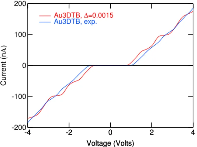
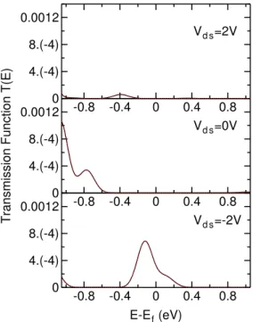
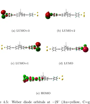
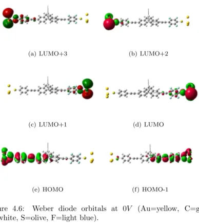
The fourth Chapter is about the calibration and application of the FOXY code to molecular species of interest. After the calibra-tion, we were able to study in detail molecular rectifiers and switches proposed in the literature. The first example is a device which has been experimentally measured by Weber et al.5 We have been able to reproduce the experimental I/V curves and to explain the under-lying rectification mechanism. We then studied binuclear transition metal complexes of the VIII group, where the metallic moieties are bridged by aromatic ligands, and we found that they do not present particularly pronounced rectifying behaviour, with rectification ra-tios in the order of ∼ 2 in the best cases. However, the introduc-tion of electron-withdrawing substituents increased and stabilized the rectification ratios over a broader range of voltages, still being far from values which can be useful in real electronic applications. The third class of devices consist in two molecular switches based on a slightly modified diarylethene moiety, which changes from an high conductive state to a low one by the means of an external opti-cal stimulus. We were able to reproduce experimental ON and OFF currents for both switches, and we were able to explain the switching effect by means of transmission function and orbital analysis.
The fifth Chapter concludes this Thesis, summarizing the key findings.
The entire work was done under the supervision of Prof. Vin-cenzo Barone, Prof. Ivo Cacelli and Dr. Alessandr Ferretti, at the
Istituto di Chimica dei Composti Organo-Metallici (ICCOM), of the Consiglio Nazionale delle Ricerche (CNR), in Pisa.
Chapter 2
Molecular Electronics
Historians tell us that in ancient times musicians, actors and painters went from court to court following the most interesting jobs by the powerful Lords. From here the common and famous expression: what is the state of the art now?
Matteo Piccardo In present-day electronic circuits, data processing, storage and transmission are obtained using a specific class of devices based on MOSFET (Metal-Oxide -Semiconductor Field-Effect Transistor) technology, exploiting the interplay of metal/oxide/semiconductor interfaces. The most important device in modern integrated circuits (IC), designed with this technology, is the transistor.
Between the different types of semiconductor devices proposed in the past, only the MOSFET emerged as a viable solution to the many requirements that a semiconductor device needs to have, and they were the only class of devices capable of an increase of the
8 formances with a constant dimension reduction, following a strict scaling law.
Fig. 2.1 shows the basic structure of a MOSFET. There are two P-N junctions that are called source and drain respectively. The drain supplies the device with electrons, while the source drags them away from the central channel region (an initially non-conducting re-gion between the source and drain very close to the silicon surface). The name Field-Effect Transistor (or FET) refers to the fact that the gate (the third contact, above the central channel) turns the transistor “on” and “off” with an electric field through the oxide: when a positive voltage is applied to the gate, electrons from the silicon bulk are attracted to the transistor channel. When the gate voltage becomes sufficiently positively charged, enough electrons are pulled into the channel from the bulk to establish a charged path be-tween the source and the drain. Electrons flow across the transistor channel, and the voltage-controlled switch is conducting. If a 0 or a very small voltage is placed on the gate, no electrons (or at least very few) are attracted to the channel. The source and drain are disconnected, no current flows across the channel, and the switch is not conducting.
A transistor is a device that presents a high input resistance to the signal source, drawing little input power, and a low resistance to the output circuit, capable of supplying a large current to drive the circuit load. Fig. 2.1 also shows the MOSFET IV characteristics. Depending on the gate voltage, the MOSFET can be “of” (con-ducting only a very small off-state leakage current, Iof f) or “on” (conducting a large on-state current, Ion).
Transistors are traditionally been made from bulk materials. This means that in order to increase performance gains and com-plexity, as the famous Moore’s Law1(the historical integrated circuit scaling cadence and reduction of cost/function law) predicts, their size should shrink following the rules of device scaling. As the struc-ture of the device decreases, the transistor building process must be controlled to a precision of a few atoms for the devices to work properly. This “bulk approach” (also called “top-down” approach),
9
Source
Gate
Drain
Metal Oxide P-type semiconductor N+ N+ Idrain Vdrain Ion Vg=0V Ioff Vg=1.8V(a)
(b)
Figure 2.1: (a): basic field-effect transistor (MOSFET) structure; (b): ideal MOSFET I/V characteristics
in which devices are usually built from lithographic methods, is be-coming more and more demanding and expensive, other than slowly approaching the inherent limitations on the control level of the build-ing process. In order to circumvent the problem, one can think of new paradigms for systems architecture that are capable of meeting the same requirements that the MOSFET device are capable now (and will be capable up to the near future) still with a scaling of the dimension of the device itself and a reduction of the power usage, sticking with the “top-down” approach outlined above.
It is then possible to think of radically change the approach in building nanodevices: instead of creating structures by removing or applying material after a pattern scaffold, the device is ideally built in a chemistry lab, atom by atom. In this way a large number of copies are made simultaneously while the composition of the sys-tems are controlled down to the last atom. This approach is called “bottom-up”.
It is clear that molecules are well suited to become focal element of a new class of devices built by employing “bottom-up approaches”.
10 The smaller dimensions and the electronic properties that character-ize these systems make molecules good candidates to become basic blocks for future electronics. “Molecular Electronics” is, therefore, the discipline that aims to reproduce conventional electronic circuit elements with molecules, hoping to reach performances comparable to the present-day Silicon-based devices. Molecular electronics is conceptually different from conventional solid state semiconductor electronics. It allows chemical engineering of organic molecules with their physical and electronic properties tailored by synthetic meth-ods, bringing a new dimension in design flexibility that does not exist in typical inorganic electronic materials. In contrast with the typical “top-dow” approach in the fabrication of solid-state devices, molecules are synthesized from the bottom (bottom-up approach), which means that small structures can be fabricated, starting from the bottom, from the molecular or single device level. It in principle allows a very precise positioning of collections of atoms or molecules with specific functionalities. Also, chemical synthesis can, in prin-ciple, make large quantities of molecular devices with relative low cost (lesser than the one for modern micro- or nano-lithography currently used for semiconductor devices fabrication) and prepare molecules with structures possessing desired electronic configura-tions and attach/interconnect them into an electronic circuit using surface attachment techniques like self-assembly.6 Self-assembly is a phenomenon in which atoms and molecules or group of molecules arrange themselves in ordered patterns without external interven-tion.
The design and development of electronic devices exploiting molec-ular functionalities has been a challenging task for chemists, physi-cists and engineers for the last few decades.7–10 Although several conceptual and technological problems still make the realization of working molecular-based devices a far off goal, the fascinating diver-sity of molecules, and thus the possibility of designing and synthe-sizing molecular species purposely tailored for specific functions, is sufficient to justify the intense effort spent in the field. For example, negative differential resistance devices4and rectifiers11have already
11 been demonstrated at the molecular level, as well as fully functional transistors12, memories and logic gates.13, 14
Transport through molecule presents peculiar features in general different from the one seen in standard metals or semiconductors. The main reason is that with molecules we don’t work with Fermi surfaces but with a defined number of discrete energy levels. The na-ture and lineup of the molecular levels with the Fermi energy of the electrodes determine most of the transport properties. In absence of any coupling between the molecule and the continuum of states pro-vided by the electrodes, both the energy levels of the molecule and the Fermi level of the electrodes will align with a common vacuum level. In this case the system is characterised by the work func-tion (W F ) of the electrodes and both the ionisafunc-tion potential (IP ) and the electron affinity (EA) of the molecule. The only way the molecule and the electrode can exchange electrons is to provide an external energy comparable to either IP − W F or W F − EA.
In contrast, the interaction between the molecular levels and the metallic contacts has the effect of broadening and shifting the molec-ular levels. In the extreme limit of large coupling, extended states spanning through the entire system (electrode plus molecule) can oc-cur and the molecular device will behave as a good conductor. The effect of an external bias is to shift the electrochemical potentials of the electrodes relative to each other by eV , with V the external volt-age and e the electron charge. Roughly speaking, a current starts to flow if some broadened occupied or virtual levels are inside the formed bias window.
There are several techniques available to date for manipulating and contacting single molecules to macroscopic electrodes in order to investigate their functionalities. However, the computational mod-elling and theoretical understanding of the various processes still suffers from several difficulties which often do not allow a compari-son between experimental and computational data, due to discrep-ancies of one or two orders of magnitude.15, 16 Charge transport in single molecules is indeed a very complex problem and results from the interplay of several basic physical effects. Any simplification of
2.1 Molecular requirements for electronic conduction 12 the problem without loosing essential physical content is therefore a very hard task.
2.1
Molecular requirements for
electronic conduction
The two basic requirements for electronic conduction in a generic material are:
• a continuous system of a large number of strongly interacting
atomic orbitals leading to the formation of electronic band structures;
• the presence of an insufficient number of electrons to fill these
bands.
In inorganic semiconductors and metals, the atomic orbitals of each atom in the crystalline structure of the material overlap, creating a number of continuous energy bands, and the electrons, initially per-tained to each atom, are delocalized across the entire structure. The strength of interaction between the overlapping orbitals determines the extent of delocalization, giving rise to the bandwidth. Likewise, in a molecule, a set of overlapping delocalized electronic states across the entire molecule is necessary for electronic conduction.
Conjugation, in molecular electronics, is an important property that is usually sought, in order to have molecules capable of pro-viding a substantial current (at least in the order of nA) in output.
π-conjugated molecules contain systems of alternating single and
double bonds. sp2or sp3 hybridisation of parallel p atomic orbitals leads to the formation of diffuse bonding orbitals in the plane of the sigma bond (a double bond). Multiple equivalent structures exist de-pending on which permutation of alternating bonds are considered. These contributing structures can mix together forming a hybrid structure at a lower energy due to the increased delocalization of
2.1 Molecular requirements for electronic conduction 13 the electrons. Conjugation within aromatic structures leads to high stability and planarity, the ring of connected p-orbitals from the sp2 hybrid carbons forming a shared volume of electron density above and below the plane of the ring.
In conjugated molecular electronic materials, the charge carriers occupy these extended molecular orbitals. The diffuse nature of the conjugated π orbitals results in sufficient overlap for charge transfer. Also, these extended orbitals easily overlap with electrodes’ states, resulting in orbitals delocalized over all the extended structure (elec-trodes plus molecule). Large regions of delocalized charge carrying orbitals mean that electrons can cross a large region of space in fewer hops. These hops are the rate limiting step that decide macro-scopic electron mobilities. Larger regions of charge delocalisation, and greater electronic wavefunction overlap between systems would be expected to lead to larger mobilities.
The performance of molecular electronic materials is highly de-pendent on the purity of the material produced. Defects and con-tamination tends to form charge traps which severely degrades per-formance. The performance is also highly dependent on processing conditions used by the device fabricator. It can take many years of effort working on improving a chemical synthesis, and simultane-ously optimising devices to know whether a material is intrinsically better than the state of the art.
Apart from consideration about conjugation, for a molecule to be useful for electronic applications, it must be addressable. This mean that it must remain in the physical location in space where it is placed. There are two important concerns in this regard. First, it is presently somewhat difficult to position molecules exactly where they are desired. Certainly there are examples of both atomic and single molecular positioning, however, these examples have not been focused at limiting the long-term propensity of the molecule to dif-fuse. Also, a primary consideration of any molecular electronic can-didate must be that of chemical stability. It is important to under-stand the long-term stability of any molecular electronics component under a wide variety of conditions. If a molecule tends to
decom-2.2 Computational strategies for molecular devices 14 pose when exposed to elevated temperatures, then it is not a good candidate for use in a molecular electronic device. Similarly, the species must be inert with regards to other molecules of the same type, a requirement that is particularly important in devices involv-ing charge-storage or redox-active molecules. Species that show poor insulation from each other would tend to exchange stored electrons, scrambling any data represented by the storage of those electrons. Conversely, a molecule which shows an irreversible electron transfer would not be a good candidate for any sort of molecular electronic device as the point of electronics is to utilize reversible charge trans-fer from one element to the next. Finally, describing a molecule doing some useful function does not automatically make it a molec-ular electronic device. There must be a way to interact with the component, both on a microscopic level and through input from the macroscopic world. Thus it is important to consider how a molecular electronic device can be “wired up”. It must be able to exchange in-formation, or transfer states to other molecular electronic devices, or it must be able to interface with the components in the system that are not nanoscopic. These requirements present challenges which are just beginning to be addressed.
2.2
Computational strategies for
molecular devices
From the molecular electronics point of view, the goal is to determine the I/V characteristic of a device that mainly consists in a central molecular region coupled with two semi-infinite metallic electrodes which are under the influence of an external bias. This is made with the aim of understanding and optimizing its characteristics and features. Before describing in detail the quantum-mechanical techniques used for this task, it is necessary to find a simple model that describes the underlying physics of a metal/molecule junction.
2.2 Computational strategies for molecular devices 15 Electronic transport through molecular devices significantly dif-fers from the one through macroscopic heterostructures. In the lat-ter, the effective mass approximation is, in general, satisfactory, due to the periodicity of the overall structure and the great mean free path length (which is the average distance travelled by a moving elec-trons without experiencing scattering events) for the electron that travel across the system. On the contrary, in a molecular device the electrons interact with a relatively small set of atoms, whose spatial position is important. Therefore, the effective mass approach fails to describe correctly the system, and the electronic structure of the molecular device should be explicitly taken into account. Frequently, Density Functional Theory (DFT) is used in order to calculate elec-tronic properties for these kind of systems.17, 18 DFT theory states that the entire problem of finding the many-body wavefunction is re-duced to that of calculating the equilibrium charge density ρ(r), via the Hohenberg-Kohn theorems, that state that, given the solution of the Schr¨odinger equation, and given the ground state (assumed non-degenerate), the external potential, and hence the total energy, is a unique functional of the electron density ρ, and the density that min-imises the total energy is the exact ground state density. Also, the Kohn-Sham method maps the entire problem onto a non-interacting one, introducing a system of non-interacting electrons that gener-ates the same electron density as the interacting one. So, thanks to the Kohn-Sham method, the entire DFT problem can be formu-lated as a ground-state, single-particle problem, and energies and eigenvalues can be calculated. However, conventional DFT methods are best suited for systems in which the total number of particles is conserved. Also, DFT presents some well known problems that could lead to discrepancies between computed and measured data. For instance, one of the most used theories for electronic transport through molecules (described in detail in the next chapter), after reducing the overall open, infinite and out of equilibrium problem to a closed and finite one, requires an accurate estimate of the energy levels, both occupied and virtual. The choice of DFT for electronic structure calculation might then introduce uncertainties or even lead
2.2 Computational strategies for molecular devices 16 to fake results.
Lang et al.19, 20 proposed a method for which, using a jellium model for the metallic electrodes in a electrode/molecule/electrode system, it is possible to map the Kohn-Sham equation of the system onto the Lippman-Schwinger scattering equation, and then solve the equations in a self-consistent way for the scattering states. Then the current will be calculated summing up each scattering state contri-bution to electron flow, with an approach similar to the one used in the Landauer-B¨uttiker theory (described in the next chapter). This model is simple, but limited: for example, it cannot correctly anal-yse strongly directional bonds as it occurs in semiconductors and in transition metal compounds. This results in a lack of evaluation of charge transfer between electrodes and the central molecule, which is a very important quantity in transport problems.
Another possibility is to implement Landauer-B¨uttiker transport theory directly.7, 8, 21 In this model, electrons transmit from one electrode to the other through the central scattering region by a series of scattering events which limit the transmission probability of each electron (described by the transmission function). The net current is then obtained integrating over the energy range defined by the Fermi level of the system and the applied bias, the trans-mission function. This theory poses its foundations on a series of approximations, one of which is that electron interactions have been included only at the mean-field level. In fact, DFT is usually em-ployed for the calculations of the electronic properties of the system. This is quite a strong approximation, especially in nanojunctions, where large current densities are common. In order to calculate the transmission function, a Non-Equilibrium Green’s Function (NEGF) specific formulation that regards steady-state transport is used. In general, this technique allows the calculation of coherent transport properties in a complete self-consistent way. In order to properly treat charge transfer phenomena, electrodes and central region are treated on the same footing, and some part of the electrodes (few atoms to some layers of atoms) should be included in the central scattering region, forming an “extended molecule”.
2.2 Computational strategies for molecular devices 17 It is also possible to implement a full Non Equilibrium Green’s Function (NEGF) method, also known as the Keldysh formalism,22, 23 which allows us, at least in principle, to solve the time-dependent Schr¨odinger equation for an interacting many-body system exactly, from which one can, in principle, calculate the time-dependent cur-rent. This is done by solving equations of motion for specific time-dependent Greens functions, from which the physical properties of interest, such as the charge and current densities, can be obtained. Even this methodology is based on some assumptions: it applies only to closed systems (so it is necessary to find a way to effectively close an open problem such as the transport one), and it needs that the total Hamiltonian is described by an unperturbed Hamiltonian plus a perturbation switched on adiabatically at a certain time (the per-turbation can be, for instance, an external field). Other than that, as in the Landauer-B¨uttiker method, in order to get the steady-state total current, it is necessary to introduce other approximations: for example we have to assume non-interacting electrons, but this time only in the leads. So, in essence, the Non Equilibrium Green’s Func-tion formalism for steady-state transport problems helps to deal with many-body interaction in the central region, not treating such inter-action at the mean-field level, in order to get more information on the transport process. The method makes large use of the contour-ordered Keldysh Green’s function:
G(r, t, r′, t′) =−i ℏ⟨Tc [ ψH(r, t)ψ†H(r′, t′) ] ⟩ (2.1)
where ψH(r, t) is the field operators written in Heisemberg repre-sentation (with respect to the total perturbed Hamiltonian bH) and Tc is the time-ordering operator. The theory also makes use of the lesser Green’s functions bG< (that stem from the general Keldysh Green’s function definition) and of the Keldysh equation, which is just a way to express the equation of motion of the lesser Green’s function in terms of self-energies (effective potential that represent the interaction of a single electron with all the other particles in the system). From that, it gives us a formula for calculating the total
2.2 Computational strategies for molecular devices 18 current by means of bG<and broadening (quantities that are related to self-energies, which in some way represent the broadening of the discrete central region levels):
I = ie ℏ ∫
Tr {
[ΓL(E)− ΓR(E)] G<(E)+
+ [fL(E)ΓL(E)− fR(E)ΓR(E)] [G+(E)− G−(E)] }dE
2π (2.2) Attempts have also been made to work directly with many-body wave-functions,24 and the Green’s function formalism, combined with the GW approximation25, 26(where the self-energy is calculated to lowest order in the screened interaction W ) is leaning towards overcoming the known problems related to the use of a mean-field theory for transport calculations.
As stated earlier, Landauer-NEGF method is based on the idea that the description of the electronic ground state at the DFT level is sufficient for describing the current flow through a channel, even if the system is not at equilibrium. This could lead to discrepancies between the computed data and the measured ones,27, 28 because it does not allow the inclusion of dynamical multi-state effects. Also, the most important quantities that define the transport properties of the system under study are computed with non-interacting Kohn-Sham excitation energies, which in general do not coincide with the true excitation energies. Standard NEGF-DFT theories also neglect the role of vibrational degrees of freedom, whose coupling to the electronic motion may indeed be relevant (e.g. molecular resistance) and is now also under active study. Excitation energies of inter-acting systems are accessible via time-dependent (TD) DFT.29, 30 In this theory, the time-dependent density of an interacting system moving in an external, time-dependent local potential can be cal-culated via a fictitious system of non-interacting electrons moving in a local, effective time-dependent potential. Therefore, this the-ory is in principle well suited for the treatment of non-equilibrium transport problems.31–34 Time-dependent simulations of current-carrying molecular devices are required to describe the transient
re-2.2 Computational strategies for molecular devices 19 sponse to an external perturbation. There is an increasing interest in time-dependent (TD) simulations of current-carrying molecular devices, from a variety of points of view.32–42 In general, time-dependent approaches can address the problems related to the use of a ground-state steady-state theories (and, in particular, aim at a better quantitatively agreement with experiment), as well as un-derline the transient response of nanoscale junctions and better de-scribe excited states (particularly useful if interested in the analysis of optical switches, where an external light pulse can variate the transmission properties of selected molecules). Usually, the whole treatment starts from the Liouville equation for the system:
∂bρ ∂t = 1 ıℏ [ b H [bρ] , bρ ] (2.3) where bρ = bρ(t) is the reduced one-electron density matrix and bH[bρ]
is a generic one-electron Hamiltonian (such as the one produced by time-dependent density functional theory). In a TD-DFT picture, we are sure that, if the system is partitioned, then the total parti-cle current between the regions computed from one-electron density matrix is formally exact.36, 43 Without something that guarantees a continual supply of electrons that have flown across the junction back into the starting electrode, the system would rapidly return in equilibrium. This is avoided by maintaining the charge imbalance, and hence the current, in the system by a driving term operating at the density matrix level:
∂bρ ∂t = 1 ıℏ [ b H [bρ] , bρ ] − Γ (bρ− bρ0) (2.4) where Γ here just represents the driving term which maintains the charge imbalance at the boundary of the transport region. Other approaches are based on the direct time propagation of the wave-function. This approaches can be interesting because one can exploit the advanced computational methods that have been developed to solve the time-dependent Kohn-Sham equations. Even here, one
2.2 Computational strategies for molecular devices 20 of the main challenges is the proper treatment of boundary condi-tions: one way to address this problem is to employ specific bound-ary potentials.32, 44, 45 These potentials are typically local in space, purely imaginary, with negative imaginary part, they vanish inside the transport region and grow rapidly away from that region. The negative imaginary part will cause asymptotic damping of resonant eigenfunctions, preventing them to extend to infinity. Because these potential effectively absorb particles that would otherwise escape to infinity, they are known as complex absorbing potentials (CAP). An-other basic issue with time-dependent DFT approaches is that most exchange-correlation functionals have been derived under equilib-rium conditions and their application to non-equilibequilib-rium problems should be analysed in more detail.
Chapter 3
Electron Transport in
Nanostructures
One single advice should be given to those who want to leave their footprints, in Science or in Arts: if you are giving birth to a new theory or movement, make sure its name will sound good in German.
Nicola De Mitri In order to address the transport problem at the nanoscale level, a full quantum-mechanical approach is needed. At the atomic level, classical description of physical systems gives way to quantum me-chanics, and in some cases, special relativity, and when modelling atomic scale circuits, one must introduce a treatment in terms of wave functions and transmission probabilities, an aspect usually ig-nored in conventional electronic engineering. In classical theory, the
22 resistance of a material is defined by Ohm’s Law:
V = RI (3.1)
where V is the external voltage, R the resistance and I the current flowing in the system. Leaving the geometrical details of the sample in consideration apart, Eq.3.1 may also be written as:
E = ρj (3.2)
in which the resistivity ρ is defined as the proportionality constant between the field E applied to our system and the current density
j. Inverting Eq.3.1, we get:
I = GV (3.3)
where G is the conductance. We can easily see that, in this classical picture of the electrical properties of a system, there is a linear rela-tion between the applied field and the generated current density: a variation of the field produce a variation in the current density which is proportional to the applied voltage by means of the resistivity.
Assuming an uniform conductor, with resistivity ρ, length l and cross-section S, we can calculate the constant voltage drop across the conductor as V = El, the total current then is I = Sj and we can calculate the resistance of the system as:
R = ρl
S (3.4)
This classical relation states that, for Ohmic conductors, the re-sistance is proportional to the length of the conductor, and inversely proportional to the cross-section. So, in the classical model, it seems that, “playing” with the parameters, it is possible to indefinitely lower the value of the resistance.
As the precision of measuring instrument rose in time, and new techniques were exploited in order to fabricate smaller and smaller conductors, new experiments on conductance of mesoscopic and
23 nanoscopic conductors were performed. What emerged from the ex-periment was a different picture with respect to what was foreseeable from the classical description of conduction. The work of van Wees
et al.46 is the first example of experimental study on conductance of mesoscopic systems (in this case, conductance of quantum point contacts in the two-electron gas of high-mobility GaAs-AlGaAs het-erostructures). The results showed clearly that the conductance was quantized in multiples of the fundamental quantity e2/πℏ. There-fore, the classical theory of conduction needed to be revisited in order to explain this novel quantum effect.
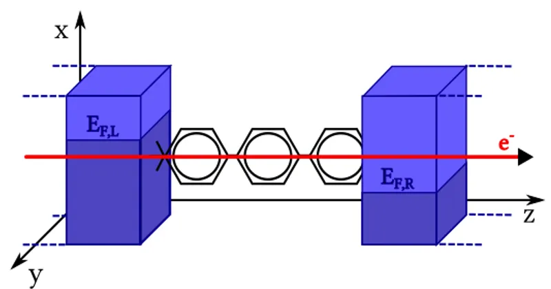
The typical setup, when dealing with nanoscopic electron trans-port problems, consists in a channel region (either a nanostructure, a solid state device, a monolayer of molecules or a single molecule) sandwiched between two metallic regions (electrodes, considered as semi-infinite due to the fact that their dimension is much bigger than the one of the channel). An external voltage is applied to the elec-trodes, and a current starts to flow in the channel region. It is clear that the system is intrinsically open (due to the external voltages), semi-infinite (due to the presence of the electrodes), and out of equi-librium (in order to ensure a current flow, the voltages applied to the electrodes must be different). It is then clear that approximations are needed in order to treat the problem from a computational point of view. The main idea is, therefore, to calculate the transmission probability that an electron can tunnel across the junction, from one electrode to the other, under the influence of an external bias that maintains the entire (open, semi-infinite) system out of equilibrium. One of the possible way to address this problem is to start with a good description of the central channel region (by a suitable Hamil-tonian) and then use the Green’s function method, coupled with the Landauer-B¨uttiker model for quantum transport in mesoscopic or nanoscopic systems.47–50
3.1 Landauer-B¨uttiker model 24
3.1
Landauer-B¨
uttiker model
The Landauer formalism21is a simple phenomenological one-electron model which dose not take into account the inelastic processes or the electron-electron interaction, but still it has been very powerful to explain several mesoscopic phenomena, and it also helps to under-stand the nature of conductance at atomic level.
The whole method poses its foundation on a number of approxi-mations regarding the overall problem. The first assumption here is that a unique steady-state solution for the current is reached. Here, in fact, we do not work with time-dependent densities, but with time-independent ρ(r), as if we have effectively reached a stationary solution (if it exists, which is, in theory, not assured) after enough time. Once the problem has been made ideally stationary, the role of the electrodes (or reservoirs) is to continually prepare electrons that move across the junction, without changing in time. They also have to be “reflectionless”, that is, the electrons can enter them from the conductor without suffering reflections. We then assume to switch from an open problem to a closed one via a set of boundary con-ditions that are usually called scattering boundary concon-ditions, with electrons that arrive without scattering from the electrodes, scatter through the junction and then move away from the junction, with-out further scattering. It is also required by the Landauer-B¨uttiker method to treat the many-body problem with a ground-state mean-field theory, even if the system is not in its ground state and there are, usually, complicated many-body interactions. Other than that, the theory assumes that every transmission channel is independent, or better assumes that the system has somehow evolved in a totally incoherent (independent) set of (single-particle) channels, populated with a Fermi-Dirac statistics. All of these are rather strict approxi-mation that we have to introduce in order to solve the problem, and neither of them are guaranteed to be satisfied in a nanojunction. So the whole theory, soon to be outlined, should be used with particular care.
3.1 Landauer-B¨uttiker model 25 As a first step, let us consider the left and right reservoirs, each at a specific electrochemical potential µL and µR, respectively, and defined by Hamiltonians HL and HR. They can be viewed as ideal blocks of conducting material with a constant transversal confining potential along its axis. The quantum mechanical solution for the wavefunction of such systems gives electron states, which are plane waves along the wire axis and standing waves in the transversal di-rection. Let us also suppose that the current flows in the z didi-rection. The energy dispersion relation for the electrodes is (see for example Fig. 3.1):
Eα(k) = ϵα+ℏ 2k2
2m (3.5)
where k is the wave vector in the axis direction and ϵαis the energy of the α-th transverse wave function. Also, given an energy E, the number of transverse modes at that energy is:
NC(E) = ∑
α
Θ(E− ϵα) (3.6)
with Θ the Heaviside step function. Now that we have defined the solution at the boundaries, we need to find the general solution for the whole system, which is defined by single-particle Hamiltonian
HS. This Hamiltonian satisfies the asymptotic conditions: lim
z→−∞HS = HL (3.7)
lim
z→+∞HS = HR (3.8)
So, the eigensolutions of HS should asymptotically merge with the ones obtained for the electrodes (plane waves along the wire axis and standing waves in the transversal direction). We can now, as an example, take an electron coming from the left lead, with energy Ei and eigenstate|ψi,ki⟩ (with ℏki its momentum). This electron then
experiences certain scattering events (whose nature is not important) due to the contact. Starting from a single wave, after the scattering process, in the right electrode this state will be a linear combination
3.1 Landauer-B¨uttiker model 26
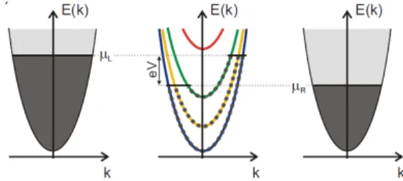
Figure 3.1: Energy dispersion and occupation of the states in the system. In the leads the quasi-continuous transversal modes are filled up to their chemical potential. Due to the small transversal dimension in the ballistic conductor only a few modes are occupied, and the +k/− k states have different fillings (dark grey dotted line) depending on which electrode they arrive from.
of transmitted waves|ψf,kf⟩ (N
R
C represents the channels at energy
Ei in the right lead):
|Ψi,ki⟩ −→ NR C ∑ f =1 Tif|ψf,kf⟩ (3.9)
In the same way, after the scattering event we expect the solution in the left lead to be a combination of the incident wave and a sum of the reflected waves at the same energy Ei of the incoming wave:
|Ψi,ki⟩ −→ |ψi,ki⟩ + NL C ∑ f =1 Rif|ψf,kf⟩ (3.10)
Since we have assumed that we have reached a steady state, the current carried by the state |Ψi,ki⟩ cannot depend on the position,
on our system, of the surface at which we evaluate it. We can then observe the current deep in the left lead or deep in the right lead.
3.1 Landauer-B¨uttiker model 27 For the left and right lead we have, respectively:
IL(Ei) = Ii(Ei) 1 − NL c ∑ f =1 Rif(Ei) (3.11) IR(Ei) = Ii(Ei) NR c ∑ f =1 Tif(Ei) (3.12)
where IL(Ei) and IR(Ei) are calculated from the general quantum-mechanical definition of the current density:
j = ℏ 2mi ( Ψ∗dΨ dz − dΨ∗ dz Ψ ) (3.13) using |Ψi,ki⟩ as the current-carrying state. In the same way, we
defined Ii(Ei) and If(Ei) as the current densities from single eigen-states |ψi,ki⟩ and |ψf,kf⟩ in coordinate representation which, after
some algebraic steps, become:
Ii(Ei) = ℏk i mLz = vi(ki) Lz (3.14) If(Ei) = ℏk f mLz =vf(kf) Lz (3.15) with Lz the length of the central region. Rif and Tif represent the reflection and transmission probability for a wave (with momentum ℏki) incident to the central region to be reflected back in the left lead (with momentum ℏkf and same energy) and to be transmitted to the right lead (again, with momentumℏkf and same energy). They are defined by:
Rif(Ei)≡ |Rif|2|I f(Ei)| |Ii(Ei)| (3.16) Tif(Ei)≡ |Tif|2 |If(Ei)| |Ii(Ei)| (3.17)
3.1 Landauer-B¨uttiker model 28 which, due to the fact that we are postulating the existence of a steady state, have the property:
NcR ∑ f =1 Tif(Ei) + NcL ∑ f =1 Rif(Ei) = 1 (3.18)
Note that the entire theory described up to now can be rewritten starting from a wave coming from the right lead, and the results do not change. Also, due to time-reversal symmetry, the indexes in Tif and Rif are interchangeable.
To calculate the total current, we must sum over all the trans-mitted and reflected waves. The density of states per spin for a momentum ℏki is:
Di(Ei) ==
Lz 2πℏvi(ki)
(3.19) the voltage V applied to the system causes, due to the assumptions initially made, a shift in the Fermi levels of the electrode by the relation eV = µL−µR, the electrons in the electrodes follow a Fermi-Dirac distribution at the electrochemical potentials µL,R. The total current is then: I = 2e ∫ { fL(E) NL c ∑ i=1 NR c ∑ f =1 Di(Ei)Ii(Ei)Tif(Ei) −fR(E) NR c ∑ i=1 Di(Ei)Ii(Ei) 1 − NR c ∑ f =1 Rif(Ei) } dE (3.20)
Defining TLR and TRL as:
TLR= NcL ∑ i=1 NcR ∑ f =1 Tif(Ei) (3.21) TRL= NcR ∑ i=1 NcL ∑ f =1 Tif(Ei) (3.22)
3.2 Transmission function evaluation 29 and, considering that the particle flux must be conserved:
TRL(E) = TLR(E) = T (E) (3.23) we finally get the expression for the total current in the Landauer B¨uttiker picture:
I(V ) = 2e h
∫ +∞ −∞
[fL(E)− fR(E)] T (E)dE (3.24)
3.2
Transmission function evaluation
According to the Landauer-B¨uttiker model, described in the pre-vious Section, the net current flowing across a junction sandwiched between two metallic, semi-infinite contacts with electrochemical po-tentials µL(R) (L=left, R=right), as pictured in Fig. 3.2 can be expressed as:
I(V ) = 2e h
∫ +∞ −∞
T (E, V ) [fL(E)− fR(E)] dE (3.25) where fL, fR are the Fermi distribution for the left and right elec-trodes∗, V is the external bias and T (E, V ) is the transmission func-tion.
Eq.3.25 is usually written in a simplified formula, in which the Fermi statistic is taken just as a step function:
I(V ) = 2e h ∫ µR µL T (E, V )dE (3.26) where µL = εf − V/2, µR = εf+ V /2, eV = (µL− µR) and εF is the Fermi energy of the entire system.
∗Fermi-Dirac statistics for the left and right electrodes: f L(R) =
1
3.2 Transmission function evaluation 30
y
z
E
F,RFigure 3.2: Schematic representation of the transport problem: two reservoirs at thermal equilibrium with a Fermi level εF are coupled to a central (confined) region. Upon an external bias applied to the electrodes, electrons start to flow.
To define a proper expression for the transmission function, it is necessary to start from the whole open system and divide it into three regions: L and R represent the two semi-infinite contacts, and
C represents the channel region, sandwiched between the contacts. If
we call ˆHS the Hamiltonian of the whole system, we could partition it in the three regions defined above, and assume that L and C are coupled by some potential ( bVLC+ bVLC† ), while regions C and R, by a potential ( bVCR+ bVCR† ), with bVLC and bVCR interaction operators. It is also assumed that L and R are decoupled†, which means V LR =
V RL = 0.
The isolated leads are described by the Hamiltonians bHL and b
HR, and it is possible to associate them with a Green’s function ( bGL
3.2 Transmission function evaluation 31 and bGR), according to
b
G(z) = bI
(z− bH) (3.27)
where z is a complex variable, bI is the identity and bH represents a
generic Hamiltonian.
With these partitions in mind, it is possible to rewrite the total Hamiltonian as: b HL VbLC 0 b VLC† HbC VbCR† 0 VbCR HbR |φ|φCL⟩⟩ |φR⟩ = E |φ|φCL⟩⟩ |φR⟩ (3.28)
where the φs are the single-particle wave functions associated to the three regions. Solving Eq.3.28 gives:
b HL|φL⟩ + bVLC|φC⟩ = E|φL⟩ (3.29) b VLC† |φL⟩ + bHC|φC⟩ + bVCR† |φR⟩ = E|φC⟩ (3.30) b VCR|φC⟩ + bHR|φR⟩ = E|φR⟩ (3.31) Rearranging the equations, it is possible to define φL and φRin terms of the Green’s function of the left and the right contact:
|φL⟩ = bGL(z) bVLC|φC⟩ (3.32)
|φR⟩ = bGR(z) bVCR|φC⟩ (3.33) Now, simply substituting Eq.3.32 and Eq.3.33 in Eq.3.30, we can express the new eigenstates of the channel region in the presence of the contacts:
[
E− bHC− bVLC† GbLVbLC− bVCR† GbRVbCR ]
|φC⟩ = 0 (3.34) We define the self-energy operators for the left and right elec-trodes as:
3.2 Transmission function evaluation 32
Figure 3.3: Regions in which the system is divided, as in 3.28. The proper central region (Channel) is the nanojunction plus part of the electrode. “Left” and “Right” are the parts which describe the true semi-infinite electrodes.
bΣR(z) = bVCR† GbRVbCR (3.36) These terms (that depend also on the external bias V through the terms bVLCand bVCR) represent an “effective” potential added to the Hamiltonian of the central region to take account of the interac-tions between semi-infinite contacts and the channel, and to switch between an open problem (due to the presence of the semi-infinite leads) to a closed one. Note that these terms are not Hermitian, so the eigenvalues |φC⟩ are not real any more: since the eigenvalue spectrum of bHL and bHR is continuous, the discrete states εk of the channel broaden into resonances peaked around their corresponding eigenvalue, their starting energy is therefore shifted (or renormal-ized) by the presence of the electrodes, and the electrons acquire a finite lifetime to scatter from the channel into one of the electrodes, due to the broadening effect mentioned before. We can, in fact, consider an “effective” Hamiltonian bHef f = bHC+ bΣL+ bΣR, whose
3.2 Transmission function evaluation 33 eigenstates can be written as:
[ b
HC+ bΣL+ bΣR ]
|Ψi⟩ = ϵi|Ψi⟩ (3.37) whose eigenvalues are, as said before, complex:
ϵi= ϵi,0− ∆i− i (γ i 2 ) (3.38) Here, ϵi,0 is the eigenenergy of the isolated conductor described by
b
HC. The time dependence of an eigenstate of bHef f has the form:
exp [ −iϵit ℏ ] −→ exp [ −i(ϵi,0− ∆i) t ℏ ] exp [ −γit ℏ ] (3.39) ∆i represents the shift in energy due to the modification of the dynamics of an electron inside the conductor by the interaction with the leads. On the other hand, the imaginary part of the energy, γi, reflects the fact that an electron injected anywhere in the conductor will eventually disappear through one of the leads stretching out to infinity. Taking the squared magnitude of the wavefunction we obtain the probability:
|Ψi|2exp [ −2γit ℏ ] (3.40) The quantity 2ℏ/γi this represents the lifetime, or the average time an electron remains in the state i before it escapes out into the leads. If the Hamiltonian would have been Hermitian, the lifetime would have been infinite.
Both Eq.3.35 and Eq.3.36 depend on the complex variable z =
E ± iδ (with δ as a positive infinitesimal constant). These
equa-tions, in fact, define two self-energy operators. We are interested only in the one depending on z = E + iδ, or the retarded self-energy operator since, roughly speaking, the retarded solution (and the re-tarded Green’s function to it related) is associated to the idea of an excitation which gives rise to “outgoing” travelling waves from the
3.2 Transmission function evaluation 34 excitation itself (the excitation being the interaction potential and the wave travelling in the positive z direction the “outgoing” wave from this excitation):
bΣL(R)(z) = bΣL(R)(E + iε) (3.41) Now it is possible to recast Eq.3.34 as:
[
E− bHC− bΣL(E)− bΣR(E) ]
|φC⟩ = 0 (3.42) and it is also possible to associate a retarded Green’s function to this differential matrix equation:
b
G(E) = bI
E− bHC− bΣL(E)− bΣR(E)
(3.43)
Given the self-energy operators, it is easy to define also the
broad-ening matrices as the imaginary part of the self-energy operators,
which are related to the broadening of the eigenstates: bΓL(R)(E) = i
[
bΣL(R)(E)− bΣ†L(R)(E) ]
(3.44) In order to calculate the current, the only thing missing is an expression for the transmission function. This problem can be re-solved relating all the theory explained above to scattering theory. The straightforward relation is to express scattered wave functions by means of the Lippman-Schwinger equation:
|Ψ+ i,ki⟩ = |ψi,ki⟩ + bG + 0Vb|Ψ + i,ki⟩ (3.45) |Ψ− i,ki⟩ = |ψi,ki⟩ + bG − 0Vb|Ψ−i,ki⟩ (3.46) with |Ψ+i,k
i⟩ representing a combination of an incident wave plus
a linear combination of outgoing waves, and |Ψ−i,k
3.2 Transmission function evaluation 35 combination of an outgoing wave plus a linear combination of in-coming waves. The scattering potential bV is simply (with bVC the potential of the central region):
b
V = bVC+ bVLC+ bVLC† + bVCR+ bVCR† (3.47) Given these equation, it is possible to rewrite the transmission and reflection probabilities, and in general, rewrite outgoing and incoming flux amplitudes. The relation between these flux amplitude is defined by the so-calledS (scattering) matrix:
S = [ r t′ t r′ ] (3.48) which connects the amplitudes of the outgoing and incoming waves in the nanojunction by the transmission and reflection matrices t and
r. It is then possible to rewrite the total transmission coefficients in
terms of the element of the S matrix:
TLR(E) = TRL(E) = Tr{tt
′
} = Tr{t′t} (3.49) Knowing the form of the Green’s function, it is then possible to rewrite the transmission function (explicitly considering the depen-dence on the external bias) with known quantities as:
T (E, V ) = Trace
[
bΓL(E, V ) bG(E, V )bΓR(E, V ) bG†(E, V ) ]
(3.50) Now, simply integrating Eq.3.50 as in Eq.3.26 we obtain the de-sired current.
It is clear that the picture here described focuses on the idea that the electrons, with a series of scattering events, cross the cen-tral region with a probability T (E, V ), by the means of transmis-sion channels provided by available energy level in the central region that, due to the interaction with the electrodes continuum and the presence of an external bias, that shifts the Fermi level of the afore-mentioned electrodes, move and broaden, as long as they interact
3.2 Transmission function evaluation 36
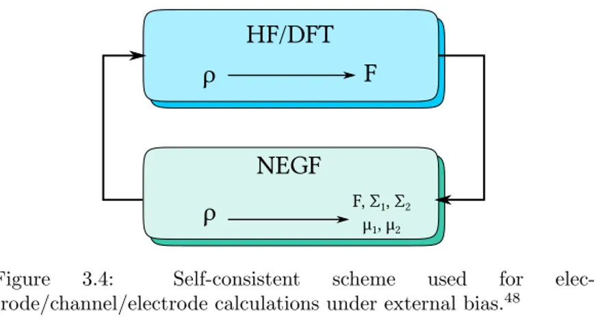
NEGF
Figure 3.4: Self-consistent scheme used for elec-trode/channel/electrode calculations under external bias.48
with the leads. Energy levels that do not couple with lead states do not broaden into resonances, and are not “available” channels for the electrons to tunnel.
It is also important to remember that the whole method here described poses its foundation on a series of pretty strict approx-imations, which are not guaranteed to be satisfied for nanoscopic systems. In particular, all these approximations lead to a descrip-tion of a system in which a steady state for the current is guaranteed to exist, condition which we don’t know a priori. Also, they can only capture mean-field properties of electron dynamics, which is plausi-ble in the case of non-interacting electrons, but not very accurate in case of interacting electrons.
The usual computational procedure involves a self-consistent scheme, implemented as follows:
1. Calculate the coupling terms V and the Surface Green’s func-tion for the electrode in order to obtain self-energies and Fermi levels, with a separate, periodic calculation on bulk material; 2. After calculating the self-energies for the electrodes, calculate
3.2 Transmission function evaluation 37 b
Hef f = bHC− bΣL(E)− bΣR(E);
3. Using the eigenvalues and eigenvectors obtained at the previ-ous step, calculate Green’s function using:
b G(r, r′, E) =∑ n Φn(r)Φ∗n(r) E− εn (3.51) with Φn given by bHef fΦn= εnΦn
4. With the Green’s Function, it is possible to find the electron density using: D =−1 πℑ ∫ +∞ −∞ [ b G(E)f (E− µ) ] dE (3.52)
5. Given the density matrix, it is possible to calculate the elec-tric field ε(r) across the junction by the means of the Poisson equation:
∇ · (ε(r)E(r)) = −4πρ(r) (3.53)
with the Fermi levels (shifted by the external bias) as the boundary conditions for the differential equation;
6. Given the density matrix and the electric field across the junc-tion, the starting Hamiltonian can be updated. The cycle starts again from Point 1, until convergence is reached; 7. When convergence is reached, with the Green’s function and
the self-energy operators, the broadening matrices ΓL(R) and the transmission function T (E, V ) are ready to be calculated. After that, the transmission functions needs to be integrated between the proper bias window in order to obtain the final current.
3.3 Implementation of the method: the FOXY code 38
3.3
Implementation of the method: the
FOXY code
The previous chapter has described the Landauer-B¨uttiker theory, and the usual computational route followed in many standard elec-tron transport codes. The implementation of the Landauer theory requires a self-consistent scheme in which, after a full periodic calcu-lation on both electrodes to obtain self-energies, the effective Hamil-tonian, with the inclusion of the field term, is diagonalised at each step. The field is the result of a separate numerical solution of the Poisson equation in which the charge density is known and provided by a diagonalization of the Hamiltonian matrix obtained in the pre-vious diagonalization step.
Since the Landauer-B¨uttiker theory is, essentially, a single-parti-cle theory, it couples nicely with Density Functional Theory, which is a single-particle, mean-field and ground-state theory. But there is no clear answer to the question of how accurate is a ground state DFT calculation for our purposes, even if we make the assumption that all the approximation in the Landauer approach are satisfied (and can, in principle, provide an acceptable description of the dy-namics of the true many-body system in an ideal steady-state), and even if we could have the exact ground state DFT functional for our case. This is because we are effectively using a ground state theory for a non-equilibrium problem (electron flow from reservoirs at dif-ferent electrochemical potential).
There are many other subtle technical problems to which is best to keep an eye on. One of the main issues is the geometrical de-tails of the contact. While in mesoscopic systems a difference of few atoms does not affect the total current in a significant way, in nanoscopic system even a single-atom change in the configuration of the junction can lead to very large differences in the current,51 mainly due to partial electronic screening, that can cause large vari-ations in the electrostatic potential at the contact region. This is why a good geometry optimization step is always required before
3.3 Implementation of the method: the FOXY code 39 a transport calculation. And, even in the case of a good geometry optimization step available, there are not experimental informations which can help in determining the exact local geometry between the single molecule and the electrodes.
Moreover, there are problems related to the calculation of the electrostatic potential in the central region. Solving the Poisson equation requires boundary conditions: due to the partitioning of the system, as defined in the previous Section, the potential at the interface between electrodes and central region is the required condi-tion. Since the Landauer approach assumes that the electrodes are, in fact, reservoirs, they have well defined electrochemical potentials,
µL and µR, eventually shifted by an external bias. In order to use
µL and µR as boundary conditions for the Poisson equation, many layers of electrode atoms are needed to be included in the calcu-lation of the central region, so to move far away from the contact region, “screen” the effects introduced by the contact itself, and, in the outermost part of the central region (the one directly connected to the reservoirs), reach a “bulk-like” behaviour.
It is then clear that modified self-consistent DFT calculations on such complex structures (such as the one described in the pre-vious Section), with hundreds of atoms, are cumbersome and time consuming, both for the calculation of the optimal geometry of the junction, and for the ground-state calculations. Most of the time, these type of calculations give also overestimated results,52, 53due to the geometrical reasons explained above, and also due to the funda-mental problems related to the use of DFT (namely, self-interaction problem54–56and excited state evaluation). Notice that a full calcu-lation is needed for every different voltage applied to the system.
One may then focus on the response of the contacted molecule to an external bias rather than on the two metallic contacts and the complex molecule-lead interface and consider an approximate approach that simplifies the metal-molecule interaction. In this way it is possible to put the attention on the behaviour of the molecule itself and on the molecular reasons which lead to, for example, rec-tification and switching phenomena. The goal, then, is to set up a
3.3 Implementation of the method: the FOXY code 40 low-cost computational approach which may be applied with confi-dence to a large variety of devices, simplifying the metal-molecule interaction while retaining all the essential physics of the charge transport due to the molecular bridge.
The approach here used is to combine Density Functional The-ory calculations for the molecular system, with the Non-Equilibrium Green’s Function Method (NEGF) and the Landauer-B¨uttiker for-malism for quantum transport in nanostructures, in a simplified way, as implemented in the domestic FOXY code.57 This simplified tech-nique has been created with the idea of developing a computationally efficient method for the calculation of I/V characteristics, which can be applied to a wider variety of molecular systems. This may allow a rapid, but reliable, investigation of molecules of potential applica-tion in electronic devices for their funcapplica-tionality.
The choice of Density Functional Theory as the main tool to calculate electronic properties of the central region means that we are going to use an effective ground state, single-particle Hamilto-nian for the system even if the problem is intrinsically a many-body one, and out of equilibrium. Also, it implies the choice of a suitable exchange-correlation functional (which, however, are usually tailored for ground-state calculations).
We have applied an approximate treatment of the molecule-lead interaction whereas the voltage bias has been accounted for through a constant electric field. Starting from the method by Gonzales et
al.,58 where the molecule-lead coupling is taken independent from the energy and proportional to the projection of the molecular or-bitals onto the terminal fragments of the molecule in between, we have developed the method described below. This approach can also be seen as a simplified derivation of the one based on the frontier orbitals of Ref.59 and by virtue of its simplicity, its range of appli-cation may be thought to cover quite large molecular species.
According to the Newns-Anderson model,60, 61 adopted in the paper of Gonzales et al.,58 we consider the interaction of a number of discrete orbitals φ of the molecule under study with a continuum of states ϕε (normalized: ⟨ϕε|ϕ
′
ε⟩ = δ(ε − ε
′