multilayered 6LiF-single crystal chemical vapor deposition diamond
detectors
S. Almaviva, M. Angelone, Marco Marinelli, E. Milani, M. Pillon et al.
Citation: J. Appl. Phys. 106, 073501 (2009); doi: 10.1063/1.3224869
View online: http://dx.doi.org/10.1063/1.3224869
View Table of Contents: http://jap.aip.org/resource/1/JAPIAU/v106/i7
Published by the American Institute of Physics.
Related Articles
Efficiency droop in AlGaInP and GaInN light-emitting diodes Appl. Phys. Lett. 100, 111106 (2012)
Dominant ultraviolet electroluminescence from p-ZnO:As/n-SiC(6H) heterojunction light-emitting diodes Appl. Phys. Lett. 100, 101112 (2012)
High 5.2 peak-to-valley current ratio in Si/SiGe resonant interband tunnel diodes grown by chemical vapor deposition
Appl. Phys. Lett. 100, 092104 (2012)
Characterization of germanium/silicon p–n junction fabricated by low temperature direct wafer bonding and layer exfoliation
Appl. Phys. Lett. 100, 092102 (2012)
AlGaN-based ultraviolet light-emitting diodes using fluorine-doped indium tin oxide electrodes Appl. Phys. Lett. 100, 081110 (2012)
Additional information on J. Appl. Phys.
Journal Homepage: http://jap.aip.org/
Journal Information: http://jap.aip.org/about/about_the_journal
Top downloads: http://jap.aip.org/features/most_downloaded
Characterization of damage induced by heavy neutron irradiation
on multilayered
6LiF-single crystal chemical vapor deposition
diamond detectors
S. Almaviva,1M. Angelone,2Marco Marinelli,1E. Milani,1,a兲M. Pillon,2G. Prestopino,1
A. Tucciarone,1C. Verona,1and G. Verona-Rinati1
1
Dipartimento di Ingegneria Meccanica, Università di Roma “Tor Vergata,” Via del Politecnico 1, I-00133 Roma, Italy
2
Associazione EURATOM-ENEA sulla Fusione, Via E. Fermi 45, I-00044 Frascati, Roma, Italy
共Received 9 April 2009; accepted 12 August 2009; published online 2 October 2009兲
High performance neutron detectors sensitive to both thermal and fast neutrons are of great interest to monitor the high neutron flux produced, e.g., by fission and fusion reactors. An obvious requirement for such an application is neutron irradiation hardness. This is why diamond based neutron detectors are currently under test in some of these facilities. In this paper the damaging effects induced in chemical vapor deposition共CVD兲 diamond based detectors by a neutron fluence of⬃2⫻1016 neutrons/cm2have been studied and significant changes in spectroscopic, electrical, and optical properties have been observed. The detectors are fabricated using high quality synthetic
CVD single crystal diamond using the p-type/intrinsic/Schottky metal/6LiF layered structure
recently proposed by Marinelli et al. 关Appl. Phys. Lett. 89, 143509 共2006兲兴, which allows
simultaneous detection of thermal and fast neutrons. Neutron radiation hardness up to at least 2 ⫻1014 n/cm2fast共14 MeV兲 neutron fluence has been confirmed so far 关see Pillon et al., 共Fusion
Eng. Des. 82, 1174 共2007兲兴. However, at the much higher neutron fluence of ⬃2
⫻1016 neutrons/cm2damage is observed. The detector response to 5.5 MeV241
Am␣-particles still shows a well resolved ␣-peak, thus confirming the good radiation hardness of the device but a remarkable degradation and a significant instability with time of charge collection efficiency and energy resolution arise. Symmetric, nearly Ohmic I-V 共current-voltage兲 characteristics have been recorded from the metal/intrinsic/p-doped diamond layered structure, which before neutron irradiation acted as a Schottky barrier diode with a strong rectifying behavior. The nature and the distribution of the radiation induced damage have been deeply examined by means of cathodoluminescence spectroscopy. A more heavily damaged area into the intrinsic diamond at the same position and with the same extension of the6LiF layer has been found, the increased damage being ascribed to the highly ionizing particles produced in the 6LiF layer by thermal neutrons through the nuclear reaction6Li共n,␣兲T. © 2009 American Institute of Physics.
关doi:10.1063/1.3224869兴
I. INTRODUCTION
Recently, neutron detectors based on synthetic single
crystal diamond 共SCD兲 have been used to measure the
neu-tron production on large experimental fusion machines1,2and fission reactors.3,4 The outstanding tolerance for hostile en-vironments, where high temperatures, high radiation fluxes, chemical corrosion, etc. compromise the operation of tradi-tionally used detectors, makes diamond an excellent material for the fabrication of high performance devices.5–8 Besides, the tendency in nuclear physics experiments is toward even higher radiation fluxes and energies, so that commercially available neutron flux monitors will soon be unable to oper-ate for a long time in such critical environments. Diamond based neutron detectors are therefore of great interest for monitoring the neutron flux in fission and fusion reactors, spallation sources, large accelerators, etc.
Compact solid-state detectors based on chemical vapor
deposition 共CVD兲 synthetic SCD with very good and
repro-ducible characteristics have been produced at Rome “Tor Vergata” University Laboratories and characterized under high flux irradiation of neutrons and ␥ rays.3 These devices have been used to detect both thermal and fast neutrons
pro-duced by the TRIGA共Training, Research, Isotopes, General
Atomics兲 fission research reactor at ENEA Casaccia 共Italy兲 and by the Joint European Torus fusion reactor at Culham 共Great Britain兲. They showed high response stability, ⬍1% energy resolution, 100% charge collection efficiency共CCE兲, excellent reproducibility and radiation hardness up to a neu-tron fluence of at least 2⫻1014 n/cm2.4,9,10
Considerable effort has been devoted in literature to highlight the degradation of the spectroscopic properties of diamond based detectors due to damage produced by heavy
neutron irradiation in natural single crystal11 or
polycrystalline12 and synthetic high pressure, high tempera-ture共HPHT兲13diamonds. However, there is a lack of studies on detector-grade CVD synthetic SCDs. CVD diamond based detectors are probably the best choice to overcome the
a兲Electronic mail: [email protected].
JOURNAL OF APPLIED PHYSICS 106, 073501共2009兲
problems connected with the use of natural共rare, expensive and not reproducible兲 and HPHT 共not detector grade兲 dia-monds. In this paper we have therefore examined the effects of such induced damages on one of our detectors after neu-tron irradiation up to ⬃2⫻1016 n/cm2 by means of its
re-sponse to alpha particles, electrical properties analysis, and
cathodoluminescence 共CL兲 spectroscopy. A good agreement
between the calculated neutron damage and the experimental results has been found.
II. EXPERIMENTAL SETUP A. Detector
The detector has been fabricated using a layered struc-ture whose details are reported elsewhere.4In short, through a two step microwave plasma enhanced CVD process we
have grown upon a commercial 具100典 HPHT substrate
共⬃500 m thick兲 a highly conductive boron-doped layer
共⬃20 m thick, acceptor density of the order of 1019 cm−3兲 which is used as backing contact. Silver paste annealed at 500 ° C was then used to obtain an Ohmic contact with the boron-doped diamond layer.
This growth step has been followed by the deposition of an intrinsic SCD layer共⬃25 m thick兲 on top of which an
aluminum 共rectifying兲 contact has been thermally
evapo-rated. In this way only the high quality, detector-grade intrin-sic CVD layer acts as sensing element, no contribution com-ing from the HPHT substrate. Finally, a 95% enriched 6LiF layer共⬃3 m thick兲 has been deposited on the Al contact in order to make the device sensitive both to fast and thermal
neutrons.14 After neutron irradiation with ⬃2
⫻1016 neutrons/cm2 the sample has been chemically
pol-ished and annealed in air at 500 ° C for 2 h. A new Al contact has been evaporated on the surface of the intrinsic layer for the examination of electrical properties and response to 5.5
MeV 241Am ␣-particles. The 6LiF layer is removed after
neutron irradiation to perform damage characterization. These post-irradiation treatments are the standard ones we use to deposit contacts, new contacts being necessary after neutron irradiation because the detector had to be detached
from its case 共which was activated by irradiation兲 and in
doing so the original contact was inevitably damaged. B. Neutron irradiation setup
Neutron irradiation exposure has been performed at the TRIGA RC-1 fission research reactor of ENEA Casaccia. TRIGA RC-1 is a 1 MW pool thermal reactor, with core and reflector assemblies located at the bottom of an aluminum tank. The core diameter is 56.5 cm, while its height is 72 cm. The overall height of the tank is 7 m therefore the core is shielded by approximately 6 m of water. The detector was positioned, using a long aluminum pipe, 80 cm above the core midplane, in an outboard position within the reactor core, inside the neutron reflector. In this position the neutron flux at the maximum reactor power of 1 MW is 2.2
⫻109 neutrons cm2s. The performance of the CVD
dia-mond detector as neutron flux monitor was tested changing the reactor output power from 10 kW to 1 MW through several steps at fixed power and repeating this cycle several
times.14 After these tests the CVD diamond detector was
lowered down at the core midplane height, outboard, and irradiated for 1800 s at reactor full power of 1 MW. The integrated neutron flux absorbed by the diamond device at the end of the whole test was estimated to be about 1.73
⫻1016 neutrons/cm2, with a fast neutrons fluence 共E
n
⬎1 MeV兲 of about 3.4⫻1015 n/cm2. The fluence was
esti-mated measuring the neutron flux through a gold activation foil placed in the diamond position, prior to diamond irradia-tion. The most important contribution to the diamond ad-sorbed dose comes from the second irradiation step since the neutron flux at core midplane height is about a factor 104
higher than 80 cm above. C. CL
The CL spectra reported in this paper have been obtained at room temperature by using a “Cambridge S260” scanning electron microscope共SEM兲 as the CL excitation source. Lu-minescence has been collected from the excited face of the sample with a paraboloidal mirror, focused through a retract-able light collection system onto the entrance slit of an
“Ap-plied Photophysics f/3.4” monochromator 共1200 l/mm, 300
nm blaze兲, and measured by a photomultiplier tube 共Hamamatsu Photonics E717-21兲. The CL spectra have been
recorded in the 200–750 nm 共i.e., 6.2–1.65 eV兲 spectral
range, and have not been corrected for the wavelength-dependent response of the optical system, which sensitivity starts to decrease at about 650÷ 700 nm. The electron beam energy has been kept at 30 kV, the corresponding emitting
region in the diamond sample being about 3.5– 7 m below
the surface共the intrinsic layer is 25 m thick兲. This value is calculated using the formula ⌬e⬇共0.007–0.014兲⫻V1.825,
15
where⌬eis the depth of the emitting region in micrometers
and V the voltage of the impinging electron beam in kilo-volts.
III. RESULTS AND DISCUSSION A. Evaluation of radiation damage
The lattice damage produced in diamond by nuclear ra-diation is due to nuclear collisions and reactions which pro-duce energetic recoil atoms, charged particles, and residual nuclei. The radiation induced defects are both vacancies and displaced atoms共interstitials兲 generated by Rutherford
scat-tering and knock-on atoms 共nonionizing energy loss兲. The
energy lost to ionization 共ionizing energy loss兲 produces
damage, too.16,17A rough estimation of the number of inter-stitial atoms共i.e., of vacancies兲 formed by radiation per unit volume is obtained by multiplying the amount of the
dis-placement per atom共DPA兲 by the atomic number densityd
共d= 1.76⫻1023 cm−3 in the case of diamond兲 18
关V0兴 =d⫻ DPA, 共1兲
where the DPA can be calculated as follows.
The direct neutron induced DPA has been evaluated with the codeSPECTER共Ref.19兲 using the reference TRIGA
neu-tron spectrum at the core midplane position and assuming a Lindhard cut-off energy共i.e., the energy required to displace
an atom兲 equal to ED= 42 eV. The calculated DPA is
共3.4⫾0.7兲⫻10−6.
A second contribution to DPA in our detector comes
from the 2.73 MeV tritium ions and 2.07 MeV ␣-particles
produced by the thermal neutron interacting with 6LiF layer. This thin film acts as a converting material from thermal neutrons to highly ionizing particles through the nuclear re-action 6Li共n,␣兲T 共Q=4.8 MeV兲. These particles cross the
6LiF layer and enter the intrinsic diamond producing
dam-age. The maximum distance they can travel in diamond is
about 20 and 3.7 m for 2.73 MeV tritium ions and 2.07
MeV␣-particles respectively. So, a part of the diamond film at the center of the sample, where the 6LiF layer had been evaporated, is characterized by an additional radiation dam-age due to tritium ions and ␣-particles. To evaluate this ad-ditional contribution to damage first the total number of
6Li共n,␣兲T reactions produced by the 1.73⫻1016
neutrons/cm2 fluence has been calculated using the
inven-tory code EASY-2007 共Ref. 20兲. Then tritium ions and
␣-particles have been generated with an isotropic distribution using the6Li共n,␣兲T kinematics in a Monte Carlo simulation routine. Finally, theSRIM-2008code21has been used to estab-lish the transport of these particles across the 3 m LiF film and, for those escaping the LiF film in the diamond layer direction, their motion in the 25 m intrinsic diamond layer.
By SRIM we also calculated the full recoil cascade damage
quantities, again adopting 42 eV as the displacement energy. The results of all these calculations are gathered in Table I. From the data in Table I it can be seen that the particles produced in the LiF layer limit their damage to the part of diamond covered by this converting layer, about a 1.5 mm diameter area.
Using the above described results the number of vacan-cies formed by radiation per unit volume 共V0兲 共see Eq.共1兲兲 has been calculated for the three contributions. The results are gathered in TableII.
These concentrations of vacancies are not negligible if compared with the concentration of impurities in the active intrinsic layer before neutron irradiation 关see Sec. III D兴. Since these defects act as traps located at deep energy levels, a change in spectroscopic, electrical, and optical properties is
expected. Moreover it is evident that the amount of damage is approximately three times higher in the region of the dia-mond covered by LiF layer than outside.
In this paper, such nonuniform damage has been evi-denced and discussed by means of CL spectra analysis per-formed both in the overdamaged contact area and in the con-tactless area. The I-V characteristics and the 5.5 MeV241Am
␣-particles spectra have been measured only in the overdam-aged area through an Al contact evaporated at the center of the intrinsic layer surface, in the same position of the alumi-num contact evaporated just before neutron irradiation and covered by the6LiF layer.
B. Alpha particles spectra
The spectroscopic properties of the diamond intrinsic ac-tive layer have been tested through the pulse height analysis
共PHA兲 spectra measured under 5.5 MeV 241Am ␣-particles
irradiation. Through this basic characterization it is possible to evaluate the performances of the device in terms of CCE, energy resolution and stability 共the so-called “polarization phenomena,” i.e., the progressive degradation of CCE, count rate, and energy resolution during extended irradiation times under continuously applied voltage bias兲. Quantitative infor-mation on the damage induced by neutron irradiation has been obtained by comparing this preliminary characteriza-tion with a similar one carried out after exposicharacteriza-tion to the high neutron flux.
In Fig.1 the PHA spectra of the SCD detector under a
bias voltage VB= 200 V before and after neutron irradiation
and the corresponding variations in the average CCE and energy resolution versus the applied electric field共or applied bias voltage兲 are reported. The CCE is defined as the ratio of the measured charge Qmto the total charge Q0generated by
the ionizing particle: CCE== Qm/Q0. The Q0 value, i.e.,
the scale of the CCE, is obtained through calibration with a 100% efficiency silicon detector, and using 13.1 eV as the mean energy required to produce an electron/hole 共e/h兲 pair in diamond.8 The energy resolution is given by the ratio R = W/具典, W being the full width at half maximum and 具典 the mean value of the␣-particle response peak. After
irradia-TABLE I. Damage produced in diamond by 2.73 MeV tritium ions and 2.07 MeV␣-particles.
ION Radial range in diamond 共m兲 Straggling 共m兲 Fraction of ions entering diamond 共%兲 Produced
displacement/ion Total DPA
Statistical error
共%兲
H-3 17.8 6.01 48.6 36.7 2.45⫻10−6 1.7
He-4 4.1 1.3 38.6 59.3 3.14⫻10−6 1.8
TABLE II. Vacancies formed by radiation per unit volume.
Type of radiation Total vacancies concentration produced 共cm−3兲 Estimated error 共statistical and systematic兲
共%兲
Neutron only 5.91⫻1017 20
Neutron produced tritium ions 4.30⫻1017 10
Neutron produced alpha particles 5.51⫻1017 10
tion with ⬃2⫻1016 neutrons/cm2 there is still a
well-defined ␣-peak, but in comparison with the spectrum
ac-quired at the same bias voltage before neutron irradiation this
peak is shifted to lower efficiency values 共approximately
three times lower兲 and is much broader.
The dependencies of the energy resolution and CCE on the applied electric field reported in Fig. 1 show that both before and after neutron irradiation the response of the de-tector improves by increasing the applied bias voltage. Higher applied electric fields lead to better resolved spectra and increased collection efficiency. Both trends tend to satu-ration: the highest CCE saturation values are 100% and 47% before and after irradiation, respectively, whereas the corre-sponding energy resolution limits are 1.4% and 10.3%. Such a degradation of the detector performance共i.e., the
broaden-ing of the ␣-peak and the lowering of CCE兲 is due to the
defects produced by neutron irradiation in the material. Va-cancies and interstitials act as trap centers and lead to a de-crease in the lifetime of electrons and holes. This is equiva-lent to a decrease in CCE as collection efficiency depends on the average drift distance ␦=共e+h兲E, e and h being
the electron and hole mobilities, respectively, being the mobility weighted lifetime of electrons and holes and E the applied electric field.
The high concentration of defects induced by neutron irradiation has a further impact on the detector performance: the “polarization” phenomenon. This phenomenon has been widely studied for Si, Ge, and CdTe detectors22,23 but up to now no quantitative analysis has been reported in literature
on diamond based detectors. This phenomenon arises from changes with time in the electrical field in the active dia-mond intrinsic layer due to accumulation of space charge in deep trap levels during the application of the bias voltage.
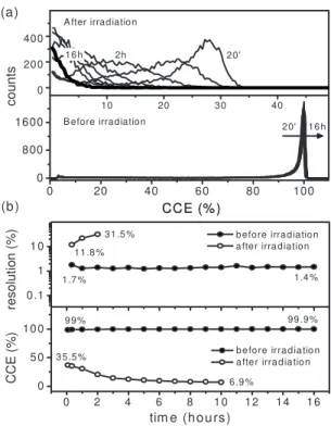
In Fig.2the time dependence of the detector response to
241Am 5.5 MeV ␣-particle, before and after neutron
irradia-tion, is reported. The sample has been biased at 150 V 共6 V/m兲 and exposed uninterruptedly to ␣-particles 共the flux being about 350 particles cm2s兲 for 16 h, the PHA
en-ergy spectra being acquired every 20 min. The time evolu-tion of the calculated average collecevolu-tion efficiency and en-ergy resolution are also shown. Before neutron irradiation the detector shows great stability within the experimental error: the energy resolution is stable at 1.7% ÷ 1.4% while CCE is 99%–100%. After neutron irradiation an evident in-stability arises: a progressive degradation of energy reso-lution and a shifting of the ␣-peak position toward low en-ergy with time after applying the bias voltage take place. After two hours the energy resolution rises from 11.8% to 31.5% and the CCE decreases exponentially in 10 h from
35.5% to 6.9% with a time constant of 2.2⫾0.2 h.
C. I-V characteristics
As described in Sec. II A, our synthetic SCD detector consists of a high purity共ideally intrinsic兲 drift layer grown on a highly boron-doped CVD diamond layer, the HPHT substrate merely acting as mechanical support for the growth of the two thin homoepitaxial layers. Ohmic contacts have been formed on the boron-doped layer whereas a rectifying aluminum contact has been evaporated on top the drift
intrin-sic layer. This structure acts as sandwich-type
metal/intrinsic/p-doped共MIP兲 Schottky barrier diode 共SBD兲.
0 5 10 15 (b) 3.2% 16% re so luti on (% ) 10.26% 1.37% 0 2 4 6 8 10 12 0 50 100 14% 90% ~ 47% CCE (%) field (V/µm) ~ 100% 0 20 40 60 80 100 0 200 400 600 (a) VB= 200V co u n ts CCE (%) VB= 200V
FIG. 1. 共a兲 PHA spectra at VBIAS= 200 V measured under 5.5 MeV241Am
␣-particle irradiation before共thicker line, filled circles兲 and after 共thinner
line, open circles兲 heavy neutron irradiation 共⬃2⫻1016 n/cm2兲 and 共b兲
CCE and energy resolution variations with applied electric field, before and after neutron irradiation.
10 20 30 40 0 200 400 (a) co u n ts 16h 2h 20' A fter irradiation 0 20 40 60 80 100 0 800 1600 CCE (% ) B efore irradiation CCE (% ) 16h 20' 0.1 1 1 0 1.7 % 1.4 %
31.5 % b efore irra diation a fter irra diation
res o lu tio n (% ) 11.8 % 0 2 4 6 8 1 0 12 14 16 0 5 0 10 0 (b) 99 .9% 9 9% 6.9% before irradiation after irradiation CCE (% ) tim e (hours) 3 5.5 %
FIG. 2. 共a兲 Time dependence of the detector efficiency to241Am 5.5 MeV
␣-particles共150 V bias voltage continuously applied兲 and 共b兲 CCE and
Due to the high breakdown electric field in the 25 m thick intrinsic layer 共⬃10 V/m兲 a significant improvement on the rectifying and on the high voltage blocking properties of the SBD has been obtained, thus reducing also the leakage current under reverse bias.
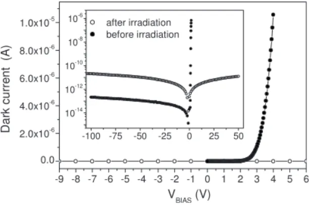
The I-V characteristics共i.e., dark current versus applied bias voltage兲 of the MIP diamond detector measured before and after heavy neutron irradiation are reported in Fig.3. The loss of the rectifying behavior after neutron irradiation is clearly evidenced by the I-V curves, which become symmet-ric with respect to the zero-bias line and nearly Ohmic. The current shows a linear increase with voltage under both for-ward and reverse bias and the corresponding series
resis-tances have been calculated to be 4⫻1012 and 4.8
⫻1012 ⍀. Therefore, after neutron irradiation the
reverse-bias regime, which corresponds to the operative reverse-bias condi-tions of the device when used as nuclear detector, increased by about two orders of magnitude, as can be observed in the inset of Fig.3where a semilog plot of the I-V characteristics is reported. The noise that affects the␣-particles PHA spec-tra reported in the previous section, giving rise to counts at 0 energy, is due to such an increment in the leakage current under reverse polarization. This noise has not been found by evaporating an Al contact outside the central overdamaged area of the intrinsic layer, where the leakage current under reverse bias is one order of magnitude lower, although the rectifying behavior under forward polarization has been lost here too.
The changes in the electrical properties that have been just described and in particular the loss of the strong rectify-ing behavior seen before the damagrectify-ing irradiation are due to the high density of deep, probably donorlike traps induced by neutron irradiation into the bulk of the intrinsic layer. The significant higher values of both forward and reverse leakage currents measured inside the central area of the sample can be ascribed to the additional defects created here by 2.73
MeV tritium ions and 2.07 MeV ␣-particles produced into
the 6LiF layer during irradiation. Anyway, little is known about the electrical behavior of radiation induced defects in diamond. Several studies on the conduction mechanisms which give rise to the I-V curves of unirradiated diamond based MIP SBDs are reported in literature24–26 but no work has been carried out on the effects of neutron irradiation on the electrical properties of such specific devices. Changes in
the I-V characteristics after neutron irradiation on
free-standing HPHT SCD with Ohmic contacts,13 p-doped/
intrinsic/p-doped diodes based on both single crystal and
polycrystalline diamond,27 and CVD polycrystalline
dia-mond detectors28have already been reported. Further work is necessary to explain the complex, not uniformly distributed changes in the conduction mechanisms observed after neu-tron irradiation in our detector.
D. CL spectra
CL and photoluminescence spectroscopy are among the most useful techniques for the characterization of defects in diamond. An extensive literature exists on this subject and the luminescence properties of the optical centers in both natural and synthetic diamonds, either as grown or radiation damaged, are well known and have been deeply studied. For this reason, the aim of our spectroscopic analysis consists essentially in the investigation and in a first attempt of ex-planation of the complex systems of damage which have been induced by neutron irradiation on our particular detec-tor structure共SCD diamond+6LiF layer兲. As in previous sec-tions the analysis will be based on a comparison between the optical properties of the sample before and after irradiation. In both cases a set of 10÷ 15 CL spectra have been recorded at different areas of the diamond surface and a good repro-ducibility has been found.
Two normalized CL spectra recorded before neutron ir-radiation are plotted in Fig. 4. In all areas of the sample a strong blue band A emission is observed while no significant emission associated to impurities is present, a confirmation of the high quality of the intrinsic diamond layer. However nitrogen, because of both atmospheric contamination of the CVD reactor and trace contaminants in the source gases, is inevitably incorporated at concentrations typically lower than few ppm共i.e., about 1017 cm−3兲. The nitrogen
concen-tration can be much lower in high quality samples, as we believe is the case of our films due to their good detection performance.
CVD synthetic diamonds contain nitrogen only in iso-lated substitutional lattice sites, as the relatively low tem-perature of growth共about 720 °C in our case兲 is well below -9 -8 -7 -6 -5 -4 -3 -2 -1 0 1 2 3 4 5 6 0.0 2.0x10⁻⁶ 4.0x10⁻⁶ 6.0x10⁻⁶ 8.0x10⁻⁶ 1.0x10⁻⁵ VBIAS(V) Da rk cu rre n t (A ) -100 -75 -50 -25 0 25 50 10-14 10-12 10-10 10-8 10-6 after irradiation before irradiation
FIG. 3. Leakage current vs applied bias voltage measured before 共full
circles兲 and after 共open circles兲 neutron irradiation.
2.0 2.5 3.0 3.5 4.0 4.5 5.0 5.5 0 2 4 6 8 10 12 2 1 band A x15 C Li nt en si ty ( µ A) energy (eV) 2. 88 3. 05 5.0 5.2 5.4 4. 95 5. 12 5. 27 edge emission
FIG. 4. CL spectra recorded at room temperature before neutron irradiation.
The spectrum shifted toward greater energies共curve 2兲 shows edge emission
共inset兲.
the onset for nitrogen aggregation, so we expect that in our films nitrogen mostly occurs in isolated substitutional sites rather than in aggregate A or B forms. In undoped CVD diamond films the broad band of blue luminescence origi-nates from dislocations.29The band A emission is peaked at 432 nm共i.e., 2.88 eV, curve 1兲, exception made for a single
spectrum共over more than ten兲 where it is much weaker and
shifted to higher energies, with the peak at 404 nm共i.e., 3.05 eV, curve 2兲. These changes can be due to a much lower defect concentration, perhaps related to a better local quality of the substrate surface. Besides, a clear edge emission arises in this case, as shown in the inset. The peaks are due to the intrinsic edge emission of the indirect 5.41 eV free exciton. In particular the most intense luminescence line, at 5.27 eV, is due to the recombination of the free exciton with the emis-sion of a 0.14 eV momentum-conserving transverse-optic 共TO兲 phonon. The two peaks at 5.12 and 4.95 eV are replicas of the free exciton emission at 5.27 eV and are thus attrib-uted to its recombination with the emission of one and two zero-center optic phonons, respectively, in addition to the TO phonon.
Concerning radiation induced damage, it is known that neutron irradiation up to about 1019 n/cm2 create in the
SCD lattice vacancies and small stressed regions of disor-dered carbon, whereas heavier doses共⬎1020 n/cm2兲 lead to
vitrification.30 In our case the fluence is 1.73⫻1016 n/cm2
and leads to a dramatic change in the CL spectra. Indeed lattice defects induced directly by neutrons 共vacancies and self-interstitials兲 and their combinations with pre-existing chemical and structural defects共dislocations and nitrogen at-oms兲, additional combinations of defects induced by the 500 ° C annealing 关see Sec. II A兴, together with regions of disordered carbons alter the optical properties of the dia-mond lattice giving rise to new emission systems and to a significant alteration of the spectra plotted in Fig.4.
Furthermore, as mentioned above, the radiation damage results in a homogeneous damage in the whole volume of the crystal and in an additional one in the central area of the sample due to 2.73 MeV tritium ions and to 2.07 MeV
␣-particles generated by the nuclear reactions into the con-verting 6LiF layer. The existence of these two differently damaged areas has been revealed both by SEM micrographs and by CL spectra.
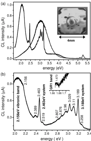
1. Area outside contact
A SEM image of the sample after neutron irradiation is reported in the inset of Fig.5共a兲together with the typical CL spectrum from points outside the central area of the sample. In agreement with Ref. 31, it is found that the broad blue band A seen before neutron irradiation is quenched by
radia-tion damage共although such quenching is not so pronounced
in a few spectra measured on the sample edges兲 and that a complex system of broad and narrow peaks arises. The na-ture of these peaks have been widely investigated by studies on radiation damage of natural and CVD SCDs, hence in this paper most of them will be explained on the basis of those consolidated and unambiguous interpretations.
In Fig. 5共b兲 the spectrum plotted in Fig. 5共a兲has been enlarged and labels added on the main peaks and on the
corresponding vibronic systems. The following spectral com-ponents have been identified共from low to high energies兲: 共a兲 a weak peak at 1.673 eV. This emission is the
zero-phonon line共ZPL兲 of the system named “GR1 centre”
i.e., isolated neutral vacancies共V0兲, which are created
when neutrons push out carbon atoms from their lattice sites. Therefore, this is an intrinsic lattice defect with no impurity involved.32
共b兲 a yellow-red component, characterized by a broad asymmetric peak extending from 1.8 to 2.3 eV with a
shoulder at 2.156 eV共575 nm兲. This orange
lumines-cence has been identified as a vibronic band with ZPL at 2.156 eV, i.e., the shoulder of the broad peak de-scribed above. This system has been attributed to a nitrogen-vacancy complex, i.e., a center that contains a vacancy and a single nitrogen atom occupying nearest neighbor sites关共Ns-V兲 center兴.
33
This nitrogen-vacancy complex can exist both in neutral共Ns-V兲0and negative
共Ns-V兲− charge states with ZPL at 575 nm共2.156 eV兲
and 637 nm共1.945 eV兲, but the 1.945 eV state does not give rise to CL, so only the intense orange emission due to the vibronic band of the ZPL at 2.156 eV is observed.34
共c兲 a narrow intense peak at 2.463 eV, preceded and fol-lowed by two weak peaks at 2.389 and 2.523 eV,
re-2.0 2.5 3.0 3.5 4.0 4.5 5.0 5.5 0.0 0.2 0.4 0.6 0.8 1.0 (a) CL int ens ity ( µ A) energy (eV) 4mm 2.0 2.2 2.4 2.6 2.8 3.0 3.2 3.4 0.3 0.6 0.9 2.15 6 (b) 2. 156 eV vibr onic band 2. 463 e V s yst e m 2. 389 2. 463 2. 519 2.807 2. 876 2. 96 3. 029 3. 11 3. 189 3. 1 88eV sys te m 3. 258 CL in te ns ity ( µ A) energy ( eV ) 1 .6 6 1 .6 8 1 .7 0 GR 1 b a n d 1.67 3 eV 1. 673 GR1 b an d 1.66 1.68 1.7
FIG. 5. 共a兲 SEM micrograph of the SCD sample after neutron irradiation
共inset兲 and CL spectrum recorded at room temperature, after annealing at 500 ° C, from points lying outside the central ring, compared with the one
obtained before irradiation共Fig.4, dotted line兲. 共b兲 Enlarged plot of the CL
spectrum in the intervals 1.97–3.41 eV and 1.66–1.70 eV共inset兲 with labels
spectively. This system is one of the most well-studied luminescence features in diamond since three different optical centers, 3H, H3, and S1, each have ZPLs close to 2.463 eV. However it has been found that these op-tical centers show different annealing, absorption and luminescence properties and are characterized by dif-ferent vibronic features, thus making possible their distinction.31,32 Furthermore, contrary to H3 and 3H systems, the S1 center is not due to radiation damage and shows a second ZPL at 2.429 eV, so only the former ones can be involved in the structure around 2.463 eV reported in Fig.5共b兲. The nature of our dia-mond and literature results leads us to believe that this luminescence at 2.463 eV is due to the 3H center. In-deed the H3 system is typically observed after radiation damage and annealing in absorption and luminescence 共both PL and CL兲 of diamonds containing nitrogen in the A aggregate form 共i.e., type Ia diamonds兲 since it has been attributed to a vacancy trapped by a nitrogen pair aggregate: the 共Ns-V-Ns兲 system.35 As discussed
above, CVD synthetic diamonds should contain mainly isolated nitrogen. It is possible that small concentra-tions of H3 centers can be grown-in during the synthe-sis of CVD diamonds through either N incorporation followed by capture of a vacancy or aggregation of single nitrogen atoms and it has been shown that high temperature treatments may thermally activate the transformation of isolated substitutional nitrogen into the A aggregate form.36 However, our sample has not been annealed at high temperature at this stage and no presence of H3 centers has been detected in the CL spectra recorded before neutron irradiation. The lumi-nescence spectrum of the H3 system is characterized by a ZPL at 2.463 eV, the major phonon replica being
at ⬃43 meV followed by a less intense one at
⬃70 meV.31
At room temperature the intensity of the ZPL is weaker than that of its first phonon replica, so at 300 K the luminescence spectrum of the H3 system should be dominated by its vibronic band.37
On the contrary the luminescence spectrum of the 3H system is characterized by a ZPL at 2.463 eV and by a single significant phonon replica at⬃70 meV,31 whose intensity at room temperature remains weaker than the one of the ZPL.38,39Such a structure matches the CL spectrum reported in Fig.5共b兲where the narrow and relative intense ZPL at 2.463 eV is followed by a weak peak at 2.389 eV, i.e., its phonon replica at
⬃72 meV. In Ref.39the feature at 2.519 eV共60 meV
above the energy of the ZPL兲 has been assigned to the 3H system共it is reported that at least six other centers show a luminescence line at energy above the ZPL兲. In earlier works this luminescence center has been as-cribed to an oxygen-vacancy pair,40 but more recent studies lead to believe the 3H center to be related to interstitials, probably the 具100典 split self-interstitial,38 although at present neither its structure, nor its charge state, nor its annealing behavior have been ultimately established.
共d兲 a luminescence system extending roughly from 2.8 to
3.2 eV with a narrow intense line at 3.189 eV: the
so-called “3.188 eV system.”41 The ZPL at 3.189 eV
and its broader and less intense phononic replica are well visible in the CL spectrum plotted in Fig.5共b兲. In particular there are four satellite lines due to the cou-pling of the ZP transition to: one 75 meV acoustic pho-non共line at ⬃3.11 eV兲, one 165 meV longitudinal
op-tic共LO兲 phonon 共line at ⬃3.029 eV兲, one LO phonon
together with one acoustic phonon共line at ⬃2.96 eV兲,
two LO phonons共line at ⬃2.87 eV兲.42The weak peak
at about 2.807 eV could be a replica of the ZPL at 3.188 eV due to two LO phonons plus one acoustic phonon, or the ZPL of another vibronic system that arises together with the 3.188 eV system after radiation damage and annealing, whose intensity, however, is at least one order of magnitude weaker.33 The 2.807 eV structure is therefore superimposed and confused on the vibronic tail of the 3.188 eV line. Anyway, both systems are ascribed to a complex that involves a single substitutional nitrogen atom共Ns兲 and a carbon
interstitial 共I兲 produced by radiation damage 关共Ns-I兲0
center兴.
The weak feature at 3.258 eV 共⬃70 meV above
the ZPL兲 is similar to the one at 2.519 eV described above and thus it could belong to the 3.188 eV system but further work is required to establish if it really does.
共e兲 a broad weak band extending from ⬃3.4 to ⬃4.5 eV 共i.e., from 270 to 360 nm兲. At room temperature this luminescence does not show any ZPL and has an asym-metric shoulder-type shape. As reported in Fig.7, after annealing at 850 ° C it shows a well-defined peak with a maximum around 3.82 eV, still without any ZPL. This band is similar in shape, energy distribution and annealing behavior to a system which is observed after radiation damage and annealing in relatively pure dia-monds: the “5RL system.” This system is characterized at 77 K by a broad band extending from 3.5 to 4.7 eV with a maximum around 3.9 eV and by a ZPL at 4.582 eV followed by sharp lines at lower energies due to the coupling of the zero-phonon transition to local-mode phonons.43Although its detailed structure has not been established yet, this center is probably associated to the carbon self-interstitials.44 In Ref. 45 it has been as-cribed to one carbon interstitial with two single substi-tutional nitrogen atoms.
2. Central area
The CL spectra measured in points lying inside the
cen-tral area are more complex. This is shown in Fig. 6 where
two spectra from these points are reported 共curves 1 and 2兲 together with the CL spectrum reported in Fig.5共a兲for com-parison. In both cases the luminescence which arises from this central area is on the whole weaker than that observed elsewhere. The majority of the spectra measured in this area show the structureless “curve 2” behavior, but a few ones still show some peaks 共“curve 1”兲. Probably, in most of the area amorphous carbon regions are formed, although locally
less damaged spots may be found. Indeed, “curve 2” spectra strongly resemble CL spectra of amorphous carbon films.46
In the following we will focus on the “curve 1” spectra, discussing the changes for all the features talked about in the previous section:
共a兲 The weak peak at 1.673 eV is still present, with no apparent qualitative changes. Its weakness prevent quantitative analysis, though.
共b兲 The intense orange band between 1.8 and 2.3 eV, due to the nitrogen-vacancy complex 关共Ns-V兲0 center兴 is
strongly quenched.
共c兲 The structure related to the 3H center appears to be substantially unvaried.
共d兲 The 3.188 eV system is still present, although less in-tense. A further quenching of the blue band A emission is also observed in this spectral region.
共e兲 The broad weak band extending from ⬃3.4 to ⬃4.9 eV is qualitatively similar, but weaker.
Furthermore, besides these well-known systems, new peaks arise, as shown in the inset of Fig.6where an enlarged plot of curve 1 is reported. In particular there are at least three main narrow peaks at 2.638, 2.2, and 2.139 eV.
Among them, only the former has been unambiguously detected in literature and it is known as the “TR12 centre,”
having ZPL at 2.638 eV and phonon replica at 2.57 eV共68
meV lower in energy兲.47
The small peak at 2.67 eV共32 meV
above the ZPL of the TR12 system兲 is known as the TR13 center and has been attributed to local modes of the TR12 center.48The defect responsible for this luminescence center is thought to involve a carbon self-interstitial complex and, maybe, vacancies.47
The narrow peak at 2.2 eV共i.e., at about 563 nm兲 is not known and at the moment no model is proposed for it. Any-way, this weak peak appears only in CL spectra recorded on the overstressed central area hence probably it is closely re-lated to the additional defects that arise there.
The peak at 2.139 eV共580 nm兲 and its phonon replica at
2.11 and 2.07 eV 共30 and 70 meV lower in energy,
respec-tively兲 could be related to the 共Ns-V兲0system, whose ZPL is
at 2.156 eV, since both systems show similar vibronic struc-tures and annealing behavior共consider that the ZPL position may be shifted by radiation induced stress and that these shifts are greater for luminescence centers which contain vacancies49兲.
The main differences among the CL spectra measured inside and outside the central overdamaged area are therefore substantially the quenching of the luminescence from 共Ns-V兲0centers and the significant reduction in the
lumines-cence from the共Ns-I兲0centers, whereas the CL from defects
related to the primary radiation damage products共vacancies and interstitials兲 seems less affected. As described earlier the additional damage in this area is due to the 2.73 MeV tritium ions and 2.07 MeV␣-particles produced by thermal neutrons into the 6LiF layer. The penetration lengths of the tritium ions and ␣-particles are 20.7 and 3.65 m, respectively. Hence, as CL emission excited by a 30 kV electron beam is located about 3.5– 7 m below the surface of the intrinsic layer, the main contribution to the change in the CL spectra seen in the central area of the sample may be ascribed almost entirely to the␣-particles.
The resulting damage consists in a sort of localized amorphization buried below the diamond surface and due to the rearrangement in disordered regions of sp2-bonded
car-bon of the interstitial carcar-bon atoms which have been ejected from their lattice sites.30,50 This situation is similar to the
damages caused by high energy 共MeV兲 ion implantation
which quench the luminescence giving rise to an increase in nonradiative recombination events in the heavily damaged regions.51Such changes in the CL spectra are thus due to an arising disorder in which vacancies and interstitials combine themselves in more complicated, mainly nonradiative, com-plexes such as vacancy clusters52and vacancy-interstitial ag-gregates.
In the central region the density of self-interstitial and vacancies is almost twice the one outside it 关see Sec. III A and Table II兴, but the related features in the CL spectra are
weaker than in the outer area. This suggests that the crystal environment is changed by this heavy damage. However, it cannot be ruled out that the quenching of the luminescence from共Ns-V兲0centers and the weakening of the luminescence
from 共Ns-I兲0 centers can be also due to a change in their
charge configuration which could lead to nonluminescent states. In this regard, it should be taken into account that during neutron irradiation a positive bias 共VB= 150 V兲 had
been continuously applied to the Al contact below the 6LiF layer, which could lead to an increase of negatively charged nonluminescent defects in proximity of the emitting region. Indeed, it is well known that no CL arises from the 1.945 eV system and from the ND1 center,31,34which respectively cor-respond to the negatively charged nitrogen-vacancy complex 关共Ns-V兲− system兴 and to the negatively charged single
va-cancy关共V兲−center兴. 2.0 2.4 2.8 3.2 3.6 4.0 4.4 4.8 5.2 5.6 6.0 0.0 0.2 0.4 0.6 I I O C L in tensi ty ( µ A) energy (eV) 2 1 2.0 2.2 2.4 2.6 2.8 2.5 7 2. 668 2.63 8 2.25 5 2. 2 2.13 9 2. 11 2.07
FIG. 6. CL spectra recorded at 300 K, after annealing at 500 ° C, from
points lying inside共“I” curves 1 and 2兲 and outside 共“O” reported for
com-parison兲 the central ring which has been pointed out from the SEM image of
the sample reported in the inset of Fig.5共a兲. In the inset an enlarged plot of
curve 1 is shown, with labels on the new peaks not observed in the CL
3. Annealing
Finally, an annealing has been performed for 2 h in flow-ing argon at 850 ° C, in an attempt to restore as much as possible the lattice order. No significant recovery of spectro-scopic and electric properties has been found. On the con-trary the CL spectra recorded from points both outside and inside the central region of the sample show noteworthy changes, as shown in Figs. 7共a兲and7共b兲, respectively. The insets show in more detail the annealing behaviors of the features共b兲, 共d兲, and 共e兲 discussed above. On the whole these behaviors are in agreement with the results reported in litera-ture on type Ib diamonds.
In particular, from both Figs. 7共a兲 and 7共b兲, the most substantial change in CL emission is the considerable in-crease in intensity of the共N-V兲0 system luminescence
关fea-ture 共b兲, 2.156 eV兴. The spectra are thus dominated by an
orange luminescence so intense to be visible to the naked eye, as also reported in Ref.33. Above about 550 ° C vacan-cies can migrate into the crystal and be trapped by single substitutional nitrogen atoms giving rise to共Ns-V兲 centers.
A more complex behavior appears in Figs.7共a兲and7共b兲 concerning the annealing effects on interstitial-related
cen-ters, i.e., features共c兲 共3H system兲, 共d兲 共self-interstitial nitro-gen system, the 3.188 eV system兲, and 共e兲 共self-interstitial, probably trapped by two substitutional nitrogen atoms兲. The emission from the 3H system 共具100典 split self-interstitial兲 is slightly reduced everywhere. Features共d兲 and 共e兲 increase in intensity more markedly in points lying inside the central overdamaged area of the sample, although the absolute in-tensity of the 3.188 eV center emission is higher in the area outside the contact, where a significant emission is observed even before the high temperature annealing. As a whole, the increase in intensity of the luminescence from interstitial-related centers is sensibly smaller than that of the vacancy related 共N-V兲0 center, probably because diffusion of self-interstitials occurs already at about 50 ° C.
Anyway, since after the annealing at 850 ° C it has been observed only an increase in intensity of the luminescence from interstitial and vacancy-related defects rather than a res-toration of the CL spectra seen before neutron irradiation, we can conclude that no appreciable annealing recovery has taken place. This is consistent with the absence of positive effects of the annealing on the electric and spectroscopic properties of the sample.
IV. CONCLUSIONS
Damage effects due to high fluence neutron irradiation have been studied for the recently proposed neutron detec-tors based on SCD grown by CVD. The detecdetec-tors use a multilayer p-type/intrinsic/Schottky metal/6LiF structure al-lowing simultaneous detection of thermal and fast neutrons. After 2⫻1016 neutrons/cm2irradiation the detector showed
a severe degradation in efficiency and energy resolution 共from 100% to 47% and from 1.4% to 10.3%, respectively兲, as well as a loss of the rectifying behavior of the Schottky contact. Such changes in the spectroscopic and electric prop-erties of the device cannot be recovered by high temperature 共850 °C兲 annealing.
A marked change in the CL spectra is also observed, additional peaks not observed before neutron irradiation aris-ing. Such peaks are attributed to various types of radiation induced defects. Interestingly, the presence of the 6LiF layer necessary for the detection of thermal neutrons leads to an additional damage in the area below the LiF layer with re-spect to regions not covered by LiF. In particular, the CL spectra measured under the LiF layer loose all the sharp fea-tures observed in spots outside the LiF covered area, resem-bling amorphous carbon CL spectra. This is explained as an additional damage due to the highly ionizing particles
pro-duced in the 6LiF layer by thermal neutrons through the
6Li共n,␣兲T nuclear reaction. Partial recovery of this damage
can be seen from CL spectra measured after high temperature annealing.
1M. Pillon, M. Angelone, D. Lattanzi, M. Marinelli, E. Milani, A.
Tuccia-rone, G. Verona-Rinati, S. Popovichev, R. M. Montereali, M. A. Vincenti,
and A. Murari,Fusion Eng. Des.82, 1174共2007兲.
2D. R. Kania, M. I. Landstrass, M. A. Piano, L. S. Pan, and S. Han,
Dia-mond Relat. Mater.2, 1012共1993兲.
3M. Marinelli, E. Milani, G. Prestopino, A. Tucciarone, C. Verona, G.
Verona-Rinati, M. Angelone, D. Lattanzi, and M. Pillon,Appl. Phys. Lett.
90, 183509共2007兲. 2.0 2.5 3.0 3.5 4.0 4.5 5.0 5.5 6.0 0 2 4 6 8 10 12 14 (a) (d) (e) CL int e n s it y ( µ A) energy (eV) (b) 4 5 0.05 0.10 0.15 0.20 3.0 0.5 1.0 1.5 2.0 5 10 15 2.0 2.5 3.0 3.5 4.0 4.5 5.0 5.5 6.0 0.0 0.4 0.8 1.2 1.6 (b) CL in te n s it y ( µ A) energy (eV) (e) (d) (b) 4 5 0.08 0.16 0.24 3.0 0.10 0.15 0.20 2.0 0.5 1.0 A A A B A B B B B A A B B A A B
FIG. 7. CL spectra recorded after annealing at 850 ° C from points lying共a兲
outside and 共b兲 inside the central area of the sample compared with the
respective CL spectra obtained before. In the insets, enlarged plots show in more detail the differences between the two spectra.
4S. Almaviva, M. Marinelli, E. Milani, G. Prestopino, A. Tucciarone, C. Verona, G. Verona-Rinati, M. Angelone, D. Lattanzi, M. Pillon, R. Rosa, Phys. Status Solidi A204, 2991共2007兲.
5J. H. Kaneko, T. Tanaka, T. Imai, Y. Tanimura, M. Katagiri, T. Nishitani,
H. Takeuchi, T. Sawamura, and T. Iida,Nucl. Instrum. Methods Phys. Res.
A505, 187共2003兲.
6G. J. Schmid, J. A. Koch, R. A. Lerche, and M. J. Moran,Nucl. Instrum.
Methods Phys. Res. A527, 554共2004兲.
7C. Mer, M. Pomorski, P. Bergonzo, D. Tromson, M. Rebisz, T. Domenech,
J. C. Vuillemin, F. Foulon, M. Nesladek, O. A. Williams, and R. B. Jack-man,Diamond Relat. Mater.13, 791共2004兲.
8M. Marinelli, E. Milani, G. Prestopino, M. Scoccia, A. Tucciarone, G.
Verona-Rinati, M. Angelone, M. Pillon, and D. Lattanzi,Appl. Phys. Lett.
89, 143509共2006兲.
9JET-EFDA Contributors, M. Angelone, D. Lattanzi, M. Pillon, M.
Marinelli, E. Milani, A. Tucciarone, G. Verona-Rinati, S. Popovichev, R.
M. Montereali, M. A. Vincenti, and A. Murari,Nucl. Instrum. Methods
Phys. Res. A595, 616共2008兲.
10M. Pillon, M. Angelone, G. Aielli, S. Almaviva, M. Marinelli, E. Milani,
G. Prestopino, A. Tucciarone, C. Verona, and G. Verona-Rinati,J. Appl.
Phys.104, 054513共2008兲.
11A. Alekseyev, V. Amosov, Yu. Kaschuck, A. Krasilnikov, D. Portnov, and
S. Tugarinov,Nucl. Instrum. Methods Phys. Res. A476, 516共2002兲.
12L. Allers, A. S. Howard, J. F. Hassard, and A. Mainwood,Diamond Relat.
Mater.6, 353共1997兲.
13T. Tanaka, J. H. Kaneko, Y. Kasugai, M. Katagiri, H. Takeuchi, T.
Nishi-tani, and T. Iida,Diamond Relat. Mater.14, 2031共2005兲.
14S. Almaviva, M. Marinelli, E. Milani, G. Prestopino, A. Tucciarone, C.
Verona, G. Verona-Rinati, M. Angelone, D. Lattanzi, M. Pillon, R. M.
Montereali, and M. A. Vincenti,J. Appl. Phys.103, 054501共2008兲.
15G. Davies, in The Properties of Diamond, edited by J. E. Field共Academic,
London, 1979兲.
16B. Campbell, W. Choudhury, A. Mainwood, M. Newton, and G. Davies,
Nucl. Instrum. Methods Phys. Res. A476, 680共2002兲.
17W. de Boer, J. Bol, A. Furgeri, S. Müller, C. Sander, E. Berdermann, M.
Pomorski, and M. Huhtinen,Phys. Status Solidi A204, 3004共2007兲.
18G. F. Knoll, Radiation Detection and Measurement, 3rd ed.共Wiley, New
York, 2000兲.
19L. R. Greenwood and R. K. Smither, “SPECTER: Neutron damage
calcu-lation for materials irradiations,” Argonne National Laboratory Report No.
ANL/FPP/TM-197, 1985 共http://www-nds.iaea.org/irdf2002/codes/
index.html兲.
20R.A. Forrest, “The European Activation System: EASY-2007 Overview,”
UKAEA Report No. UKAEA FUS 533, 2007. 21http://www.srim.org/
22H. L. Malm and M. Martini,IEEE Trans. Nucl. Sci.21, 322共1974兲.
23B. Dezillie, V. Eremin, Z. Li, and E. Verbitskaya,Nucl. Instrum. Methods
Phys. Res. A452, 440共2000兲.
24M. Brezeanu, T. Butler, N. Rupesinghe, S. J. Rashid, M. Avram, G. A. J.
Amaratunga, F. Udrea, M. Dixon, D. Twitchen, A. Garraway, D.
Cha-mund, and P. Taylor,IET Circuits Devices Syst.1, 380共2007兲.
25D.J. Twitchen, A.J. Whitehead, S.E. Coe, J. Isberg, J. Hammersberg, T.
Wikström, and E. Johansson,IEEE Trans. Electron Devices51, 826 2004.
26Q. A. Huang, D. Y. Sun, and J. K. O. Sin,Appl. Surf. Sci.171, 57共2001兲.
27A. Denisenko, W. R. Fahrner, U. Strähle, H. Hensche, and R. Job,IEEE
Trans. Nucl. Sci.43, 3081共1996兲.
28J. HassardNucl. Instrum. Methods Phys. Res. A368, 217共1995兲.
29A. T. Collins,Diamond Relat. Mater.1, 457共1992兲.
30D. T. Morelli, T. A. Perry, and J. W. Farmer,Phys. Rev. B47, 131共1993兲.
31J. Walker,Rep. Prog. Phys.42, 1605共1979兲.
32G. Davies,Proc. R. Soc. London, Ser. A336, 507共1974兲.
33A. T. Collins and S. C. Lawson,J. Phys.: Condens. Matter1, 6929共1989兲.
34K. Iakoubovskii, G. J. Adriaenssens, and M. Nesladek,J. Phys.: Condens.
Matter12, 189共2000兲.
35G. Davies, S. C. Lawson, A. T. Collins, A. Mainwood, and S. J. Sharp,
Phys. Rev. B46, 13157共1992兲.
36R. M. Chrenko, R. E. Tuft, and H. M. Strong,Nature共London兲270, 141
共1977兲.
37G. Davies,J. Phys. C7, 3797共1974兲.
38J. W. Steeds, T. J. Davis, S. J. Charles, J. M. Hayes, and J. E. Butler,
Diamond Relat. Mater.8, 1847共1999兲.
39K. Iakoubovskii, G. J. Adriaenssens, N. N. Dogadkin, and A. A. Shiryaev,
Diamond Relat. Mater.10, 18共2001兲.
40J. Walker, Inst. Phys. Conf. Ser. 31, 510共1976兲.
41A. T. Collins and G. S. Woods,J. Phys. C20, L797共1987兲.
42L. H. Robins, L. P. Cook, E. N. Farabaugh, and A. Feldman,Phys. Rev. B
39, 13367共1989兲.
43A. T. Collins, G. Davies, H. Kanda, and G. S. Woods,J. Phys. C21, 1363
共1988兲.
44A. T. Collins, P. J. Woad, G. S. Woods, and H. Kanda,Diamond Relat.
Mater.2, 136共1993兲.
45A. M. Zaitsev, Optical Properties of Diamond共Springer-Verlag, Berlin,
Heidelberg, 2001兲.
46W. J. Hsieh, C. C. Lin, U. S. Chen, Y. S. Chang, and H. C. Shih,Diamond
Relat. Mater.14, 93共2005兲.
47J. Walker,J. Phys. C10, 3031共1977兲.
48G. Davies, C. Foy, and K. O’Donnell,J. Phys. C14, 4153共1981兲.
49A. M. Zaitsev, A. A. Gippius, and V. S. Vavilov, Sov. Phys. Semicond. 16,
252共1982兲.
50J. O. Orwa, K. W. Nugent, D. N. Jamieson, and S. Prawer,Phys. Rev. B
62, 5461共2000兲.
51H. Yagyu, Y. Mori, A. Hatta, T. Ito, M. Deguchi, M. Kitabatake, T. Hirao,
and A. Hiraki,Phys. Status Solidi A154, 305共1996兲.