Scuola di Dottorato in Ingegneria “Leonardo da Vinci”
Dottorato di Ricerca in Ingegneria dell’Informazione
Noise characterization of nanoelectronic
devices
Ivan Alessio Maione
Tutore:
Prof. Massimo Macucci
Tutore:
Prof. Giovanni Basso
Tutore:
Prof. Bruno Pellegrini
Contents
Introduction 1 1 Noise 5 1.1 Thermal noise . . . 5 1.2 Shot noise . . . 8 1.2.1 Fano Factor . . . 111.2.2 Shot noise in mesoscopic system . . . 12
1.3 Generation-recombination and 1/f noise . . . . 15
2 Measurement system 19 2.1 Noise measurements . . . 20
2.1.1 Single amplifier configuration . . . 20
2.1.2 Cross correlation amplifiers . . . 22
2.1.3 Amplifying block . . . 28
2.1.4 Calibration . . . 30
2.2 Cooling down . . . 33
2.3 Mechanical insulation . . . 34
2.4 Final setup . . . 35
3 Double barrier resonant tunnel diode 41 3.1 Tunneling . . . 41
3.2 Double resonant barrier . . . 43
3.3 Noise in double-barrier structures . . . 46
4.1 Resonant tunnel diode characterization . . . 55
4.2 Choice of feedback resistors . . . 59
4.3 Cross-spectrum measurement . . . 61
4.4 Transfer function measurement . . . 64
4.5 Test and Fano factor measure . . . 67
4.6 Best performance and sensitivity limits . . . 71
4.7 Interpretation of Fano factor results . . . 73
5 Fabrication techniques 79 5.1 GaAs/AlGaAs two dimensional electron gas . . . 79
5.2 Basic Processing Techniques . . . 82
5.2.1 Mesa etching . . . 82
5.2.2 Ohmic contacts . . . 84
5.2.3 Gates photolithography . . . 87
5.2.4 Sub-micron Gates . . . 89
5.2.5 Packaging . . . 91
5.3 Freestanding double quantum dots . . . 92
5.3.1 Brief introduction . . . 92
5.3.2 Wafer structure and device design . . . 94
5.3.3 Freestanding Processing Methods . . . 95
6 Cryogenic system (down to 25 mK) 99 6.1 3He/4He dilution refrigerator . . . . 99
6.1.1 Physical principle . . . 100
6.1.2 Basic operation . . . 102
6.1.3 Cables and Microwave filter . . . 103
6.2 Measurement system . . . 105
Conclusions 109
Frequency-dependent shot noise derivation 111
Acknowledgments
It is a pleasure for me to thank all the people that have contributed to this thesis in many ways.
First of all, I would like to express my deep and sincere gratitude to my advisors. Prof. Massimo Macucci for giving me the opportunity to join his group. Among many other things he has taught me to be “so patient”. Many thanks go to Prof. Giovanni Basso for being a constant and fruitful presence, and for helping me to get through the difficult times. I am also honoured of having worked with Prof. Bruno Pellegrini, who gladly shared his knowledge and his perpetual energy and enthusiasm in research.
I want to sincerely thank Prof. Giuseppe Iannaccone for his advice and friendly help.
A gratefully acknowledgement goes to Prof. Charles G. Smith for having given me the opportunity to spend a very fruitful period in Cambridge, but also to all those people I met there, who helped me feeling at home.
I am indebted to many colleagues who have worked in this group for providing a stimulating and fun environment in which to learn and grow. Especially I am obliged to Dr. Gianluca Fiori, now as always a reference point.
I am grateful, rather in debt with Giulia Piccolo, who I esteem both as re-searcher and as person. She has always been a constant source of encouragement; her support definitely improved my job.
Among all the friends that kept close to me along these years I would like to thank particularly Marina Del Prete and Rosario Di Somma, who have been supporting me since far before I started with my PhD.
I take also a chance to thank all those people I met in these years for pleas-antly filling the time left from research.
Finally, my deepest gratitude goes to my family for their unflagging love and support throughout my life.
Introduction
Recent years have witnessed an enormous progress in fabrication techniques for the definition of electronic devices at the nanometer scale. Advances in physical and chemical synthetic approaches, like the advent of epitaxial growth techniques, molecular beam epitaxy (MBE) and metal-organic chemical vapor deposition (MOCVD), as well as the development of nanoscale lithography tech-niques (i.e. electron-beam lithography), allow to design and implement electronic systems that exhibit a range of both classical charging effects and quantum me-chanical effects.
Nanoscale systems such as quantum point contacts, quantum dots, nano-wires, single molecules, and short carbon nanotubes exhibit interesting transport characteristics [1, 2, 3, 4, 5], which are based on their discrete energy structure and on correlations in the electronic transport process. Examples of novel effects that can be observed only at nonoscale are conductance quantization [3, 6], the Coulomb blockade [7, 8], and the Kondo effect [9, 10] that, usually, can be investigated only at very low temperatures.
In this contest, noise characterization has emerged as an extraordinarily pow-erful tool to investigate aspects of transport phenomena at a very basic level. Through noise it is possible to obtain information about the structure and the transport properties of nanoscale devices that are complementary to those given by the DC characteristics and the small signal AC response. Single carrier trapping and detrapping , carriers diffusion in solids, fractionally charged quasi-particles in quantum Hall system, as well as many other phenomena have recived a clear explanation or confirmation via noise measurements [11, 12, 13].
of charge lead to the so-called shot noise. Such statistical fluctuations show up much stronger in nanosize electronic devices, compared to macroscopic classical devices, due to the small number of electrons involved in device operation. It is known from theory, as well as from experiments, that interaction effects (like the Coulomb-interaction between electrons, the Pauli exclusion principle, the phonon-electron interaction) may lead to correlations among carriers, resulting in characteristic features in the shot noise. Therefore, shot noise turns out to be sensitive to the electronic structure and the coupling strengths to the electrodes of the system, giving information on how transport occurs. For these reasons, it has raised an immense interest and has been developed into a fast growing subfield of mesoscopic physics [14, 15, 16].
When carriers are emitted into and across the device randomly, without any correlation, full shot noise is observed, with a current power spectral density
SI = 2qI, where q is the electron charge and I is the average current. This
result, as stated in Schottky’s theorem [17], is the consequence of the variance of a Poisson process being equal to its average value. The presence of correlations between carriers produces deviations from such a behavior: noise can be sup-pressed if the motion of carriers is made more regular by negative correlations or increased if fluctuations are enhanced by particle bunching [14]. The ratio of the measured shot noise power spectral density to that predicted by Schottky’s theorem is usually defined Fano factor, i.e. F = SI/Sf ull. Fano factor of 1/3
(in diffusive wires)[18, 19, 20, 21, 22], 1/4 (in chaotic cavities)[23, 24, 25] or 1/2 (for a symmetric double barrier) [26, 27], among other, have been observed.
The experimental challenge in the measurement of shot noise consists of the elimination of other sources of noise, such as thermal noise and low frequency 1/f noise due both to the device under test and to the external environment. In such measurements on semiconductor devices, it is generally very difficult to detect in a direct way noise levels associated with bias currents below a few hundred picoamperes. This is due to the fact that noise power spectral densities, corresponding to such current levels, are of the same order of magnitude or much lower than those which are characteristic of common low noise amplifiers.
To overcome this problem, many techniques for reducing the noise of the measurement system have been implemented. One technique consists in
accu-rately evaluating the noise due to the amplifier and to other spurious sources and in subtracting it from the overall noise at the output of the amplifier itself [28]. Another technique consists in using two noise amplifiers, with their input ports connected in series or in parallel with the device under test and in computing the cross correlation of the noise signals at the output of the two amplifiers: in this way the uncorrelated noise contributions are averaged out[29, 30, 31, 32]. A further technique consists in cooling down the amplifiers, in particular the feed-back resistors, in order to improve the noise figure by reducing the contribution of the thermal noise sources. A drawback of this technique consists in additional noise contributions from the cryogenic bath[29, 32].
When a very high sensitivity is required, it is necessary to setup a system based on a combination of the above three techniques, as described in this thesis.
Outline of the Thesis
This thesis is a presentation of the work that I have carried out over the three years of my PhD program at the Department of Information Engineering of the University of Pisa. It focuses on setting up of cryogenic systems for shot noise measurements with very high sensitivity. The systems were meant to be tested on different mesoscopic structures: double barrier resonant diodes, quantum point contacts, double quantum dots, and chaotic cavities. These structures should yield useful results to investigate the physics of electron transport, and to verify the validity of some theoretical models present in the literature.
This thesis is organized as follows:
Chapter 1 is a brief introduction to noise in electrical circuits. It covers thermal, shot, generation-recombination, and flicker noise. A brief classical and quantum treatment of shot noise is presented.
Chapter 2 discusses the equipment setup and the issues related to low noise measurements at cryogenic temperatures. The technique of cross correlation for noise measurement is presented.
Chapter 3 is intended as an introduction to the fundamental physics of resonant tunneling diodes. A theoretical model on shot noise in resonant double tunnel diodes is presented.
Chapter 4 is the experimental chapter which provides the description of measurements on a resonant tunneling double barrier diode. A comparison with the numerical simulation is also shown.
Chapter 5 details the fabrication of freestanding double quantum dots car-ried out at the Semiconductor Physics Group of the Cavendish Laboratory, Uni-versity of Cambridge as guest researcher.
Chapter 6 discusses the setup of a cryogenic system with a base temperature of 25 mK.
Chapter 1
Noise
Noise is a random signal. It consists of frequency components that are random in both amplitude and phase. In nature, different types of noise can occur, depend-ing on the system property (e.g. size, material, geometry) and on the conditions under which noise is observed (e.g. temperature, bias voltage, frequency).
In this chapter we will show the main noise mechanisms present in nature. In particular, we will focus our attention on thermal noise and shot noise.
1.1
Thermal noise
Thermal noise is generated by the equilibrium fluctuations of the electric current inside an electrical conductor, which happen regardless of the applied voltage. It is due to the Brownian motion of electrons. Thermal noise was first postulated by Walter Schottky in 1918 [17] and then observed by J.B. Johnson, in 1927,[33] who conducted a series of experiments showing such type of noise affects all conductors. He provided a numerical expression as well for its spectral density [34], derived also by Nyquist on 1928 [35] by means of quantum and statistical considerations.
Let us consider a conductor at non-zero temperature. Electrons move ran-domly through the conductor due to thermal fluctuations. We can characterize the occupation of a state by an occupation number n which is either zero or one.
The thermodynamic average of the occupation number hni is determined by the Fermi distribution function fE, i.e. hni = fE. On the other hand, the
probabil-ity that the state is empty is given by 1 − fE. The variance of the occupation
number reads
(n − hni)2= n2− 2nhni + hni2. (1.1)
Taking into account that for a Fermi system n2 = n, we find immediately
that the fluctuations of the occupation number at equilibrium away from its thermal average are given by
h(n − hni)2i = hn2i − 2hni2+ hni2= fE(1 − fE). (1.2)
The mean-squared fluctuations vanish in the zero temperature limit. At high temperatures and high enough energies the Fermi distribution function is much smaller than one and thus the factor 1 − fE in Eq. (1.2) can be replaced by 1.
Although the average current in the conductor resulting from these fluctua-tions is zero, instantaneously there is a current fluctuation δI that gives rise to a voltage across the terminals of the conductor. The variance of these random fluctuations is given by Nyquist’s formula
h(δI)2i = 4k
BT G∆f (1.3)
where T is the temperature, G the conductance, and f the frequency.1 This
fol-lows from the fluctuation-dissipation theorem and from the fact that in macro-scopic systems the electrons thermalize in a short time, so that the system re-mains near equilibrium even under a voltage bias.
The spectral current density SI of the noise is the mean-squared current
fluctuation per unit band width:
SI(f ) = h(δI) 2i
∆f . (1.4)
Using Eq. (1.3), the equation above reads
SI = 4kBT G. (1.5)
1Thus, the investigation of equilibrium current fluctuations provides the same information
Thus, following this treatment, we obtain a uniform spectrum that extends to all frequencies.
In Nyquist’s original derivation of thermal noise, the problem of noise in a resistor R (R = 1/G) is viewed as a simple one-dimensional case of black-body radiation. The following frequency-dependent expression for the thermal noise was calculated
SI(f ) = 4G hf
ehf /kBT − 1, (1.6)
where h is Plank’s constant. For hf << kBT , the denominator in Eq. (1.6) can
be approximated by hf /kBT and Eq. (1.5) is recovered. At room temperature
the quantum-mechanical correction applies at 6.25 THz. Since most circuits operate at frequencies that are orders of magnitude less than this value, the zero-frequency expression (S(0) = 4kBT G) for thermal noise can be used.
S(f) fc Sth(0) = 4GkBT Sth(f ) = 4G hf ehf /kBT− 1 f
Figure 1.1: Semilog plot for thermal noise according Nyquist’s theorem.
If a voltage V 6= 0 is applied across the conductor, the total noise rises above such an equilibrium value.
1.2
Shot noise
Unlike thermal noise, which is caused by thermal fluctuations, shot noise results from the discrete nature of charge transfer through a conductor.
The shot noise spectral density is proportional to the average current and, as it happens for the thermal noise, it is characterized by a white noise spectrum up to a certain cut-off frequency, which is related to the time taken for an electron to travel through the conductor.
Let us now derive the expression of the shot noise power spectrum density in the semiclassical and quantum limit, following the approach described in [14], in which a single barrier with transmission probability T and reflection probability
R = 1 − T is considered (see Fig. 1.2).
q
T
R
Figure 1.2: A current stream of unit charge q, coming from the left side of a single barrier, is partitioned into two streams of transmitted and reflected carriers with probabilities T and R = 1 − T .
If n is the number of electrons coming from the left in the time τ , and if we assume that electrons move independently one from the other, the probability distribution of transmitted electron nT is binomial and reads:
pn(nT) = Ã n nT ! TnT(1 − T )n−nT. (1.7)
We can then compute the mean value hnTi and the variance h∆n2Ti. In
for the variance, where h∆nTi = hnTi − hnTi. For perfect transmission (when
there is no barrier) the variance is equal to zero.
The current, defined as the amount of electric charge flowing through the barrier over time, is given by I = qnT/τ and its variance therefore is found to
be h∆I2i = qhIi(1 − T )/τ . If we now assume that particles cross the barrier
independently from each other in the low transmission regime (n >> 1, T << 1), Eq. (1.7) can be approximated by the Poisson distribution
pn(nT) = e−λλ nT
nT!
(1.8) where λ = nT .
The noise power spectral density S(f ) can now be obtained from the Wiener-Khintchine theorem [36], which states that S(f ) is equal to the Fourier transform of the autocorrelation function. The finite frequency noise thus takes the form
S(f ) =
Z ∞ −∞
eif th∆I(t)∆I(0) + ∆I(0)∆I(t)idt (1.9)
with ∆I(t) = I(t) − hIi. We note that only the time difference t in the current-current correlation is involved.
Let us now suppose that the particles arrive at random instants tk and that
the current pulses are independent and uncorrelated. After a time T >> tk, the
pulse looks like a delta function, and the current can be written as
I(t) =X
k
qδ(t − tk). (1.10)
Substituting Eq.( 1.10) into Eq. (1.9), the shot noise power spectrum density reads
S(f ) = 2qhIi. (1.11)
where the properties of the delta function are used to evaluate the integral. On the contrary, a frequency dependence is found in the case of current with a negligible duration. In particular, if we suppose
I(t) =X
k
with s(t) is a square current pulse of duration τc, the following power spectrum is obtained S(0) = 2qhIi · sin(2πf τc) 2πf τc ¸2 . (1.13)
A full derivation of this equation is reported in Appendix 1.
The equation above gives the same result as Eq. (1.11) at low frequencies, but has a cutoff at fc= 1/τc as shown in Fig. 1.3.
S(f) 1 τc 2 τc f S(0)= 2qI
Figure 1.3: Frequency dependence for shot noise power spectrum density.
The time τc is of the same order of the mean transit time that the electrons
spend to cross the device (∼1-100 ps in common devices), which means the cutoff frequency is about 10 GHz - 1 Thz. Therefore the approximate equation (1.11) is good for almost all integrated circuit design.
We would like to observe that in Schottky’s case the full shot noise Sf ull=
2eI is found because the granularity of the current is in term of the elementary charge q = e. This does not always have to be so. For instance, multiple charge quanta have been observed in point contact between two superconducting electrodes [37], values of q = 2e in superconductors (due to cooper-pairs) [38, 39, 40, 41] or q = e/(2m + 1) with an integer m in the fractional quantum Hall
effect [42, 43, 44, 45, 46]. This shows that shot noise can be used as a tool to measure the effective unit of charge transferred in electric devices.
1.2.1
Fano Factor
In the previous shot noise derivation, we have supposed that carriers are emitted into and across the device randomly, without any correlation. If the events are correlated, i.e. the statistic is not Poissonian, the above treatment leads to
SI 6= Sf ull. In this case, it is helpful to use a dimensionless quantity, called Fano
factor.
The Fano factor F is defined as the ratio of the actual shot noise S to the Poissonian (or full) shot noise, i.e.
F = SI Sf ull =
SI
2ehIi. (1.14) Thus, when electron transport is due to uncorrelated, independent events, the Fano factor turns out to be equal to unity, F = 1, which is referred to as a Poissonian Fano factor. In the case of a barrier at zero temperature, the above treatment leads to S = Sf ull(1−T ) and therefore F = (1−T ). Since the current
is proportional to T , we immediately see that, in the cases T = 0 and T = 1, shot noise vanishes, whereas the Fano factor can have values between 0 (e.g. ballistic conductor, T = 1) and 1 (e.g. single tunneling barrier with T << 1). For T = 1/2 the shot noise is maximal.
As we will discuss in the following section, this picture fails when further effects introduce correlations on charge transport. Deviations from F = 1 have been demonstrated to be due to statistical anti-bunching or bunching, which leads to negative or positive correlations, respectively.
For example, in fermionic systems, the Fano factor can be suppressed due the Pauli principle, leading to sub-Poissonian values F < 1, whereas, in bosonic systems, bunching leads to super-Poissonian values with F > 1.2 Beside the
Pauli principle, the Coulomb repulsion could be another source of correlations in conductor. Usually Coulomb interaction yields a sub-Poissonian statistic but,
2This statement is based on a series of assumptions (e.g. zero-impedance external circuits,
spin indipendent transport). If these conditions are not met, positive correlations could be found in fermionic systems, too.
as we will see, there are some particular situation in which it can enhance the Fano factor above 1.
1.2.2
Shot noise in mesoscopic system
In order to describe shot noise in mesoscopic systems, a quantum mechanical treatment of the transport problem is required. A simple way to obtain for-mulas for current and shot noise in this case is to use the Landauer-B¨uttiker
approach. The idea of this approach is to relate transport properties of the sys-tem to its scattering properties, which are assumed to be known from a quantum mechanical calculation.
T
T
µ
1V
lead1
lead2
x
y
Conductor
µ
2E
k
E
k
µ
1µ
2Contact 1
Contact 2
I
> 1I
< 1I
> 2I
< 2Figure 1.4: A conductor having a transmission probability of T is connected to two large contacts through two lead [taken from [1]].
Let us to consider the system shown in Fig. 1.4, made up of a conductor, considered as a scattering region, connected to electron reservoirs (contact 1 and contact 2) by means of lead 1 and lead 2. It is assumed that the reservoirs are large enough to be characterized by a temperature T1,2, and a chemical potential
µ1,2 ( µ1 > µ2 ). We assume only elastic scattering, so that the overall energy
is conserved. For N modes, the incoming and outgoing modes are related by a 2N × 2N scattering matrix S Ã I< 1 I> 2 ! = S Ã I> 1 I< 2 ! (1.15) where I>
j andIj< (j = 1, 2) are respectively the N -component vectors denoting
the amplitudes of the incoming and outgoing modes in leads 1 and 2. The scattering matrix S can be decomposed in four N × N matrices
S = Ã s11 s12 s21 s22 ! ≡ Ã r t0 t r ! . (1.16)
The blocks r and r0describe electron moving back to the left and right reservoirs,
respectively. The off-diagonal blocks t and t0 describe the electron transmission
through the sample. The flux conservation in the scattering process implies that the matrix S is unitary. In the presence of time-reversal symmetry the scattering matrix is also symmetric.
The symmetrized current I = (hI2i − hI1i)/2 can be obtained from the
equa-tion [1] I =2e h X n Z
dETn(E)[f1(E) − f2(E)]. (1.17)
Here Tn(E) are the eigenvalues of the transmission matrix t†(E)t(E), which are
interpreted as the transmission probabilities of an eigenchannel n (i.e. they are the transmission probabilities for each channel in a representation in which the transmission matrix is diagonal), while the Fermi function is defined as
fj(E) = 1
e(E−µj)/kBT + 1 (j = 1, 2). (1.18)
In the zero temperature limit and for small bias, the derivative of Eq. (1.17) with respect to bias voltage yields the Landauer’s equation for the conductance
of an N channel system G =2e 2 h N X n=1 Tn. (1.19)
Equation (1.19) shows that conductance can be expressed in terms of transmis-sion probabilities only.
An expression for shot noise can be derived by means of the Landauer-B¨uttiker formalism. Substituting Eq. (1.17) in Eq. (1.9), the following expression for the zero-frequency shot noise is derived
S = 4e2 h
X
n
Z
dE{Tn(E)[f1(E)(1 − f1(E)) + f2(E)(1 − f2(E))]+
+Tn(E)(1 − Tn(E))[f1(E) − f2(E)]2}
(1.20)
In an equilibrium situation the second part containing f1− f2 vanishes and
the formula for the power spectrum density of the thermal noise is recovered
S = 4kbT G. (1.21)
In the opposite limit, when T = 0 and a finite bias Vb = µ1− µ2 is applied,
the contribution involving fj(E)(1 − fj(E)) (j = 1, 2) vanishes and the
non-equilibrium shot noise reads
S = 2e2e 2 h V N X n=1 Tn(1 − Tn). (1.22)
The Fano factor can then be expressed as
F = PN n=1Tn(1 − Tn) PN n=1Tn . (1.23)
In the case of one channel (n = 1), we find the same result we derived in the last section for the case of a single tunneling barrier.
To sum up, thermal noise dominates at low bias eVb<< kBT , whereas
non-equilibrium shot noise is predominant at higher bias eVb>> kBT . The crossover
from thermal to shot noise is described by the expression
S = 2e 2 h " 2kBT X n T2 n+ eV coth µ eVB 2KBT ¶ X n Tn(1 − Tn) # , (1.24)
which follows from Eq. (1.20) by evaluating the energy integral [47]. In [23] the previous equation has been verified in chaotic cavities defined by two quantum point contacts in series.
1.3
Generation-recombination and 1/f noise
The generation-recombination (g-r) process is a natural part of all semiconductor behavior. In the semiconductor, carriers are set free from bonds with a particu-lar atom by a generation process, which is necessary for both of the conduction mechanisms to occur (i.e. drift and diffusion). This leaves “uncovered” donors or acceptors, which will occasionally trap a passing carrier. The continuous trap-ping and de-traptrap-ping of the charge carriers causes a fluctuation in the number of carriers in the conduction and valence bands (electron-hole pair creation). The time-scale on which these processes occur is characterized by τ (lifetime of electrons in the conduction band). The noise power spectral density assumes in a Lorentzian-like form, function of frequency [48]
S(f ) ∼ hI2i τ
1 + (2πf )2τ2. (1.25)
The power spectral density is constant at low frequency with a corner at
fc = 1/2πτ . Above this corner, the spectrum is proportional to 1/f2 (see
Fig. 1.5).
A general treatment, in which the electron number switches between discrete values at random times, which appropriately distributed time constants, leads to other types of noise, such as 1/f noise.
Thus, let us assume that the mean-square current contains many indepen-dent contributions with random relaxation times τ , with a known statistical distribution P (τ ). Averaging over all τ values, we have
S(f ) ∼ hI2i
Z ∞ 0
τ
1 + (2πf )2τ2P (τ )dτ. (1.26)
If we now assume that P (τ ) ∼ 1/τ in an interval [τ1, τ2] and that it vanishes
otherwise, we find that [49]
S(f ) ∼ hI 2i 2πf 1 ln(τ2/τ1) Z 2πf τ2 2πf τ1 dγ 1 + (γ)2, (1.27)
fc= 1/2πτ
S ∝ 1/f2
f S constant
S(f)
Figure 1.5: A typical spectrum for the generation-recombination noise. The noise power spectral density has a Lorentzian-like form as a function of frequency, characterized by a constant time τ .
implying that S(f ) ∼ 1/f in the frequency interval τ1−1<< 2πf << τ2−1. By proper choice of P (τ ) it is thus possible to account for the 1/f noise in this case, but of course the physical origin of precisely this distribution for P (τ ) remains to be determined. Experimentally, it has been found the power spectral density of this noise increases without limit as frequency decreases, following the law |f |−α, where α is more or less constant and usually lies between 0.8 and 1.4.
Thus, 1/f noise dominates ad low frequency, while it vanishes at high fre-quency. The frequency at which the 1/f and white noise contributions are equal (as shown in Fig. 1.6) is usually indicated as frequency corner (fc).
Since the 1/f noise power spectral density is inversely proportional to fre-quency, the integrated power in the spectrum between the (positive) frequencies
f1 and f2 is P (f1, f2) = Z f2 f1 S(f ) = Clnf2 f1 (1.28)
where C is the proportionality constant. This simple result shows that for a fixed frequency ratio f2/f1 the total noise power per decade of bandwidth is
S = S1/f+Sth S1/f ∝1/f Sth= 4kBT G f S(f) fc
Figure 1.6: A typical spectrum for noise in which both thermal and 1/f contri-butions are present.
constant. This property of 1/f noise is known as scale invariance.
The first observation of 1/f noise in electronic system (referred to as flicker noise) was made by Johnson, in 1925, and since then the subject has developed extensively. This is in particular due to the fact that 1/f noise occurs in many physical, biological and economic systems. In physical systems it is present in some meteorological data series, as well as in the electromagnetic radiation output of some astronomical bodies. In biological systems, it is present in heart beat rhythms and in the statistics of DNA sequences. In financial systems it is often referred to as a long memory effect.
There are many theories on the origin of 1/f noise [50, 51, 52, 53, 54]. Some theories attempt to be universal, while others are applicable to only a certain type of material, such as semiconductors [55, 56, 57, 58, 59]. Universal theories of 1/f noise are still a matter of current research.
Chapter 2
Measurement system
As stated in the Introduction, this thesis focuses on setting up a cryogenic sys-tem for shot noise measurements on mesoscopic structures, in order to study electron transport properties and quantum mechanical effects.
Usually, many of these effects (e.g. Pauli exclusion, Coulomb blockade, phonon blockade, etc.) are visible only at very low temperature because thermal fluctuations wash them out. For this reason the developed system is intended to work at cryogenic temperatures.
Two cryogenic systems have been set up: the first system allows us to perform shot noise measurements at 4.2 K and 77 K, using liquid Helium and Nitrogen to cool down the device under test (DUT); the second system uses a dilution refrigerator to reach temperatures down to 25 mK. In both systems, noise re-duction techniques are used to achieve high sensitivity.
In this chapter we will describe the first cryogenic system based on the cross correlation technique and on cooling of the feedback resistors.
2.1
Noise measurements
2.1.1
Single amplifier configuration
The traditional method used to measure the noise power spectral density of an electronic device can be described in a simple way: noise generated from the DUT1, opportunely biased, is amplified and then analyzed with a spectrum
analyzer.
In Fig. 2.1 a block diagram is shown for the two generic configurations (series and parallel) used to perform a noise characterization of the DUT.
Biasing (a) Amp DUT Spectrum Analyzer Unit (b)
DUT Amp Spectrum
Analyzer Unit
Biasing
Figure 2.1: Block diagram for noise measurement of a bipole: single amplifier configuration. The bipole is connected in (a) series and (b) parallel with the amplifier.
The noise characteristic of the DUT is determined by its equivalent current (voltage) noise source. Such source contributes, through a factor determined by the amplifying block, to the total noise at the output port of the amplifier, which
is the input for the spectrum analyzer in both configurations.
A current-voltage converter is commonly used as amplifying block for the series configuration, and a voltage amplifier for the parallel one. As a conse-quence, to maximize the contribution of DUT noise to the output voltage, the series configuration is used when the DUT impedance is larger than the amplifier input impedance, and parallel configuration in the other case.
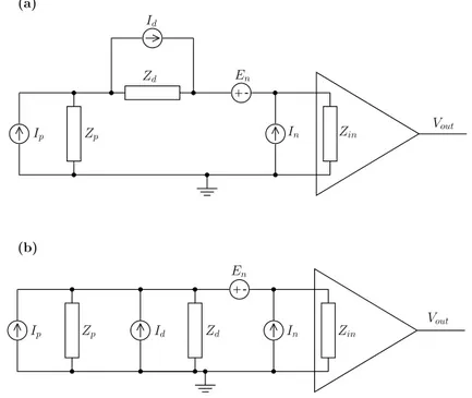
In Figure 2.2 the small signal equivalent circuits for the DUT and the am-plifiers are shown, as well as all the noise sources. In particular, the amplifier is characterized at the input by an impedance Zin, and the equivalent voltage and
current noise sources, En and In respectively. Ip, Id, Zp, and Zdare instead the
noise current source and the differential resistance of the biasing unit and of the DUT, respectively. (b) -+ Id Zd In Zin Zp Ip En Vout -+ En Id Zp Ip Vout In Zin Zd (a)
Figure 2.2: Noise representation En-In for the single amplifier (a) series and (b) parallel configuration.
Referring to the circuit in Fig. 2.2(a), the output voltage reads
Vout= Avol Zin
Zin+ Zp+ Zd[En+ (Zp+ Zd)In+ ZdId+ ZpIP] (2.1)
Thus, the power spectral density of the total noise at the output port is given by SV = |A|2(SEn+ SIn|Zd+ Zp|2+ SId|Zd| 2+ S Ip|Zp| 2), (2.2) where A is defined as A = Zin (Zin+ Zd) Avol. (2.3)
An analogous equation is obtained for a parallel configuration.
Equation (2.2) was obtained considering the noise voltage and current gen-erators completely uncorrelated. Otherwise, we have to introduce a term due to the correlation, which is SEnIn(Zd+ Zp)∗|A|2.
From Eq. (2.2) we see that the noise sensitivity of the system cannot be lower than the noise contribution of the front-end amplifier.
In very low noise level measurements the noise contribution due to the instru-mentation is comparable or even larger than what has to be measured. In such a situation, it becomes necessary to implement some noise reduction techniques that can contribute to push down the noise floor of the measuring system.
2.1.2
Cross correlation amplifiers
The cross correlation technique consists in processing the signals from two in-dependent channels, in the series or in the parallel configuration, by computing the signal cross-correlation, in order to get rid of the uncorrelated noise com-ponent of the single channels, due to the amplifier contributions. When the noise to be measured is stationary, the cross-correlation technique has proven to be effective to overcome the limitations imposed by the electronic noise of the amplifier and to extend the sensitivity of noise measurements to extremely low values [31, 60, 61].
Current configuration (series)
Figure 2.3 shows a schematic diagram of the cross correlation amplifiers in se-ries, in which the signal from the DUT is fed to two distinct and independent
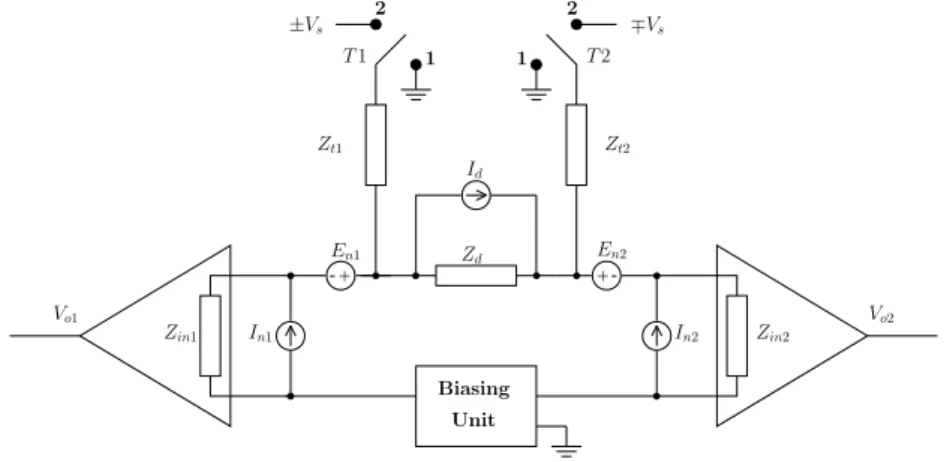
amplifiers, whose inputs are connected with the device terminals. -+ Id Zd -+ En2 1 2 1 2 ∓Vs In2 Vo1 In1 Vo2 ±Vs Zt1 Zt2 En1 Biasing Unit Zin1 Zin2 T 2 T 1
Figure 2.3: A basic scheme of the cross correlation amplifiers in a series config-uration.
The switches T1 e T2 are connected to ground, position 1 (the purpose of
Vsand the shunt impedances Zt1 and Zt2 will be clarified later in this section).
As mentioned before, Enj,Inj,Zinj (j = 1, 2) are the input parameters of the
two amplifiers, while at the output they are represented by a voltage-dependent current generator AvolVin(Vin is the voltage at the input port), and the output
impedance Zout. Zd is the DUT impedance and Id is the noise current, which is
the quantity that we would like to measure.
The noise model for the system is shown in Fig. 2.4. The amplifiers are replaced by their equivalent circuits. Zj is equal to Zinj//Ztj (j = 1, 2), while
I0
n1 and In20 are defined as follows:
In10 = In1− En1 Zd//Zt1 + En2 Zd , (2.4) I0 n2= In2− En2 Zd//Zt2 + En1 Zd . (2.5)
We underline that, until the introduction of I0
n1 and In20 , the circuit
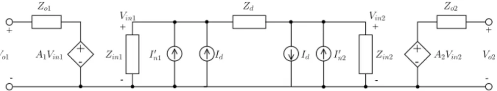
+ -+ -+ -+ -Zd Vin2 + -Zo2 + -Vo2 I0 n2 Id Zo1 Vo1 Vin1 Id I0 n1
A1Vin1 Zin1 Zin2 A2Vin2
Figure 2.4: Noise model of a cross correlation system in series configuration.
sources, on the other hand, are peculiar of the circuit itself, because their value is determined by specific relations among the circuit impedances.
Referring to Fig. 2.4, the output voltage Vo1is equal to
Vo1 = A1Vin1 = A1 Zin1(Zin2+ Zd) Zin1+ Zin2+ Zd(I 0 n1+ Id) + A1 Zin1Zin2 Zin1+ Zin2+ Zd(I 0 n2− Id),
or, using a compact form,
Vo1= A1 Zin1Zd
Zin1+ Zin2+ ZdId+ A1Vn1 (2.6)
where
Vn1= Zin1
Zin1+ Zin2+ Zd[(Zin2+ Zd)I 0 n1+ Zin2In20 ]. (2.7) While Vo2 is Vo2= A1 Zin2Zd Zin1+ Zin2+ ZdId+ A2Vn2 (2.8) where Vn2= Zin2 Zin1+ Zin2+ Zd
[(Zin1+ Zd)In20 + Zin1In10 ]. (2.9)
Taking into account that Id and Vn1 (Vn2) are uncorrelated, while Vn1 and
Vn2 are correlated, the power spectral density SVo1Vo2 is given by the following
equation: SVo1Vo2 = Vo1Vo2∗ ∆f = A1A∗2Zin1Zin2∗ |Zd|2 |Zin1+ Zin2+ Zd|2SId+ A1A ∗ 2SVn1Vn2. (2.10)
Let us, now, analyze the second term in the previous equation in order to show that it can be neglected (in a first approximation).
SVn1Vn2 is affected by En1, En2, In1, and In2. Referring to Fig. 2.5, the noise -+ Zd -+ En2 Zin2 In2 Vo1 Zin1 In1 Vo2 En1
Figure 2.5: Schematic circuit in which only the contributions En and In are represented.
contributions to the output signals due to En1 are given by
|Vo1−En1| = A1 |En1Zin1| |Zin1+ Zin2+ Zd|, |Vo2−En1| = A2 |En1Zin2| |Zin1+ Zin2+ Zd|. (2.11)
Similar expressions are found if En2 is used instead of En1. These correlated
components are seen by the two channels of the instrument in the same way as the DUT signal and can therefore not be removed. However, they can be neglected thanks to the very low input impedance of the amplifier compared to that of the device (|Zd| >> |Zin1|, |Zin2|). Thanks to the same condition, the
generators In1and In2 have an effect only on the corresponding channels. Their
output noise components are thus uncorrelated over the two channels and can be suppressed with a long enough measurement.
Equation (2.10) can thus be approximate to
SVo1Vo2 =
A1A∗2Zin1Zin2∗ |Zd|2
|Zin1+ Zin2+ Zd|2SId. (2.12)
In the next section, we will show how one can rewrite Eq. (2.12) as a func-tion of the transfer funcfunc-tions of both input channels, in order to simplify the computation of SId from experimental data.
Transfer functions
The frequency responses of the two amplifiers, H1(jω) and H2(jω), can be
mea-sured using the circuit shown in Fig. 2.3, where the switches T1e T2are placed
in position 2.
In this configuration, the choice of the input signal source is of primary importance. The signal sources ±Vs and ∓Vs have equal amplitude, opposite
sign, and a white noise spectrum. The amplitude of Vs is chosen large enough
to neglect I0
n1, whereas In20 and Id contribute to the frequency response. They
are connected to the input terminals of the amplifiers through the impedances
Zt1 and Zt2.
Figure 2.6 shows the noise equivalent circuit for the transfer fuction con-figuration. The sources Vs are replaced with their current noise sources It1 =
±Vs/Zt1 and It2 = ∓Vs/Zt2.2 + -+ -+ -+ -Zd Vin2 + -Zo2 + -Vo2 Id Zo1 Vo1 Vin1 Id A2Vin2 It1 It2 Zin1 Zin2 A1Vin1
Figure 2.6: Noise equivalent circuit for the transfer function configuration.
With the assumptions made before, the output voltages Vo1 and Vo2are
Vo1 = A1Vin1= A1It1 Zin1(Zin2+ Zd)
Zin1+ Zin2+ Zd + A1It2 Zin1Zin2 Zin1+ Zin2+ Zd = A1It1 Zin1Zd Zin1+ Zin2+ Zd + A1It1 Zin1Zin2 Zin1+ Zin2+ Zd µ 1 + It2 It1 ¶ . 2We will consider I
t1 = +Vs/Zt1 and It2= −Vs/Zt2 to calculate H1(jω), vice versa for
Vo2 = A2Vin2= A2It2 Zin2(Zin1+ Zd) Zin2+ Zin1+ Zd + A2It1 Zin1Zin2 Zin1+ Zin2+ Zd = A2It2 Zin1Zd Zin1+ Zin2+ Zd + A2It2 Zin1Zin2 Zin1+ Zin2+ Zd µ 1 + It1 It2 ¶ .
To simplify the equations, we can assume Zt1 = Zt2 = Zt. By using the
condition |Zd| >> |Zin1|, |Zin2|, we can write the following expression for H1(jω)
and H2(jω) H1(jω) = Vo1 Vs = A1Zin1Zd Zt(Zin1+ Zin2+ Zd), H2(jω) = Vo2 Vs = A1Zin2Zd Zt(Zin1+ Zin2+ Zd). (2.13)
This technique is hence useful to directly determine H1(jω) and H2(jω) in an
unambiguous way, including the effect of the unavoidable parasitic capacitance of some circuit nodes.
We can now write SVo1Vo2as a function of H1(jω) and H2(jω). It immediately
follows from Eq. (2.13) that
H1(jω)(−H2∗(jω)) =
A1A∗2Zin1Zin2∗ |Zd|2
|Zin1+ Zin2+ Zd|2|Zt|2, (2.14)
where the asterisk indicates the complex conjugate. By combining Eq. (2.12) to Eq. (2.14), the cross-spectral density between the two outputs is found to be
SVo1Vo2 = H1(jω)(−H ∗ 2(jω))|Zt|2SId (2.15) and hence SId= SVo1Vo2 H1(jω) · (−H2(jω)∗)|Zt|2 (2.16)
The same equation is obtained if a parallel configuration is used instead of a series one.
2.1.3
Amplifying block
The performance of the system in terms of sensitivity is ultimately determined by the noise characteristic of the amplifying block. For these reasons, a careful analysis of the contributions of amplifier noise sources to the output noise voltage must be performed in order to choose the best characteristics for the low noise amplifier.
In our measurement system, for the series configuration, a current-voltage converter has been implemented (see Fig. 2.7). Due to the virtual ground, the
Id Zd -+ Rf Et Rf + -Amplifying block -+ En Vout In
Figure 2.7: Schematic diagram for a current-voltage converter. Current and voltage noise generators are represented.
voltage at the output of the amplifier is
Vout= −RfId (2.17)
and the system gain is
|A| = ¯ ¯ ¯ ¯VIoutd ¯ ¯ ¯ ¯ = Rf. (2.18)
As underlined in the previous section, it is important to know the input impedance of the amplifying block in order to choose the proper configuration by means of the relation Zd >> Zin(or Zd<< Zin). With respect to Fig. 2.8,
the impedance Zinis the parallel of ZinOP and the feedback impedance reported
+ -+ -ZK I ZinOP Rf Vin AvolVin Vout Rout -+
Figure 2.8: Equivalent circuit for the current-voltage converter. The impedance
Zin is the parallel of ZINOP and the Miller equivalent of feedback impedance.
Let us start by evaluating calculate the current I
I =Vout− Vin
Rf (2.19)
and the voltage output Vout
Vout = AvolVin− RoutI (2.20)
Combining Eq. (2.19) and Eq. (2.20), the Miller coefficient K is obtained as
K = Vout Vin
= Rout− AvolRf
Rout+ Rf
. (2.21)
With a reasonable approximation, we can assume Rf >> Routand Eq. (2.21)
becomes K = −Avol. Thus, the input impedance of the converter is given by
ZK= µ Rf 1 − K ¶ //ZinOP ∼= Rf Avol (2.22)
in which the condition ZinOP >> Rf/(1 − K) is assumed.
To complete the discussion about the amplifying block, we have to calculate the noise contribution to the output signal due to the voltage and current sources
En contribution
The power spectral density of the Vout component due to En is given by
SVout−En = SEn|HEn| 2, (2.23) where HEn is HEn= Avol ZinOP ZinOP + Rf//Zd Rf+ (ZinOP//Zd) Rf + (1 + Avol)(ZinOP//Zd) . (2.24) For reasonable value of Zd, we can assume the input impedance of the
am-plifier much larger than the DUT impedance (ZinOP >> Zd). This leads to
rewriting Eq. 2.23 as SVout−En = SEn ¯ ¯ ¯ ¯Avol Rf+ Zd Rf+ (1 + Avol)Zd) ¯ ¯ ¯ ¯ 2 . (2.25) In contribution
The equivalent impedance seen by the generator In is equal to the parallel
be-tween the DUT impedance and the input impedance of the transresistive am-plifier. Thus, using (2.18), the output voltage power spectral density of the component due to In is given by
SVout−In = SIn|Rf| 2|Z
K//Zd|. (2.26)
2.1.4
Calibration
As introduced in Chapter 1, we are mainly interested in the measurement of the Fano Factor. In order to obtain its correct value, it is necessary to know accurately both the noise current power spectral density SI and the value of Id.
Such value can be obtained from Eq. (2.17) as
Id= Vout
Rf
. (2.27)
However, there are several sources of nonideality, such as the operational amplifier offset voltage, the bias current, and the uncertainties on the value of the feedback resistor for different operating temperatures. Therefore, a calibration
procedure must be performed to determine the exact relationship between the DC component of Vout and the DUT current.
Figure 2.9 shows the schematic diagram of the calibration procedure. The voltage offset introduced by the amplifier is taken into account by means of the offset voltage source Vof f.
-+ +-Vof f A V Vout Zd Id Rf VB
Figure 2.9: Schematic diagram of the calibration procedure. The voltage offset introduced by the amplifier is taken into account by means of the fictitious voltage source Vof f.
The measurement equipment for the calibration procedure consists of a pi-coammeter HP41408, used to bias the DUT and measure the polarization current
Id, and two multimeters, HP3478A and HP34401A, to measure the bias voltage
and the output voltage Vout respectively.
All the instrumentation is controlled by a computer running in a specific software, implemented by our group, which allows the acquisition and storage of the data from the picoammeter and the multimeters. In order to remove the fluctuation due to the change in the bias voltage, it is necessary to wait a few seconds between one acquisition and the next.
An example of a plot of the output voltage as a function of the measured current is shown in Fig. 2.10. The linear behavior of such calibration curve is due to the resistance Rf, according the relation in Eq. (2.27); the voltage (current)
offset of the amplifier are also observed.
Current [pA] Voltage [mV] 2.5 1.5 0.5 −0.5 2 1 0 −1 −1.5 −2 −2.5 −2 −1.5 −1 −0.5 0 0.5 1 1.5 2 Vof f Iof f
Figure 2.10: I − V characteristic achieved by the calibration procedure. The curve exhibits a linear behavior due to the resistance Rf. The current and voltage offset (Iof f and Vof f) are marked.
offset are
|Vof f| = 0.39 mV
|Iof f| = 0.41 pA
(2.28) Thus, this procedure of calibration becomes essential for very low currents: when the current Idis lower than 20 pA, an error equal to Iof fon the evaluation
of the current lead to a per cent error over 2% in the Fano factor.
It is also important to underline that there are shifts in time of the calibration curve by a fraction of a picoampere, probably due to a varying contact potential or to a small instability of the amplifier offset. So it is necessary to perform the calibration measurement before and after the noise acquisition for each single data point.
For notably small current values, corresponding to Voutvalues in the millivolt
range, it will be necessary to insert, between the operational amplifier output and the voltmeter, a low-pass filter with a time constant of a few seconds, in order to remove fluctuations around the average value.
2.2
Cooling down
The device under test is introduced in the dewar vessel containing the cryogenic liquid by means of a stainless pipe. A distance of 1-2 mm between the helium surface and the stainless steel pipe is necessary in order to avoid any additional noise due to the liquid ebullition. Thus, the lowest effective temperature at which the device can be cooled down is approximately 6 K, when using liquid helium, and 85 K when using liquid nitrogen.
In order to determine exactly the device temperature, the system is equipped with a temperature diode (Silicon Diode Thermometer Si410AA produce by Scientific Instruments), with an operating range between 300 K and 1.5 K, placed in close thermal contact with the device under test. The manufacturer provides a temperature-voltage table for a bias current of 10 µA. The curve T − V is shown in Fig. 2.11. 300 250 200 150 100 50 0 0.4 0.6 0.8 1 1.2 1.4 1.6 1.8 Temperature (K) Voltage (V) I = 10 µA
Figure 2.11: Temperature-Voltage curve for the Silicon Diode Thermometer Si410AA produce by Scientific Instruments. The diode polarization curve is set to 10 µA.
To operate the diode, the biasing circuit of Fig. 2.12 has been set up. We have used a 1.8 M Ω resistor, an Agilent E3631A power supply, a Keithley
617 picoammeter, and a multimeter HP3478A to detect the diode current and voltage drop respectively.
V A + - HP3478A HP 34401A VR R Dewar Cryogenic Temperature Diode
Figure 2.12: Biasing network for temperature diode.
In order to reduce the thermal noise introduced by the feedback resistors (and therefore the whole system noise), they are also kept in the dewar vessel, while the operational amplifiers are kept at a higher temperature to ensure a normal operation.
2.3
Mechanical insulation
While setting up the system, we have noticed that its sensitivity to mechanical vibrations transmitted from the floor turned out to be critical. Such vibrations introduce a spurious noise contribution, mainly low-frequency noise (below 10 Hz in our specific system configuration), and they are particularly disruptive for measurements performed with the highest gain (see Fig. 2.13, dotted line curve). A careful insulation of the system from mechanical vibrations has been ob-tained by means of an air cushioned structure that supports the helium dewar
with the sample holder and the cross correlation amplifiers (see Fig. 2.14). Furthermore, all coaxial cables connecting the amplifier with the sample and the feedback resistors have been clamped at several locations along the support-ing shaft, in order to prevent noise resultsupport-ing from time-varysupport-ing deformation.
With such solution, the mechanical vibration have an influence suppressed down to a level no longer distinguishable in the cross spectrum. The benefits of this improvement are well understood looking at Fig. 2.13, in which the mea-sured power spectral density before (dotted line) and after (continuous line) the inclusion of mechanical insulation are shown. The two curves are obtained for a double resonant tunnel structure (described in chapter 3), for a polarization current Id equal to 3 pA 0.1 1 10 100 1000 10−22 10−23 10−24 10−25 10−31 10−30 10−29 10−28 10−27 10−26 SI h A 2 / H z i f [Hz]
Figure 2.13: Power spectral density measured before (dotted line) and after (continuous line) the mechanical insulation.
2.4
Final setup
A block diagram of the final setup of our measurement system is shown in Fig. 2.17.
Figure 2.14: Air cushioned structure that supports the helium dewar with the sample holder and the cross correlation amplifiers.
- -+ TLC072 TLC072 DUT VB + Rnull Rnull Vout1 Vout2 Rf Rf 1 2 1 2 Ct Ct ∓Vs µA741 ±Vs T2 T1 V− C V− C Vs R R V+ C V+ C
Figure 2.15: Final schematic diagram of the cross correlation configuration.
amplifier based on a µA741 amplifier.3 V
s and −Vs are injected by means of
the capacitors CT (with a value of about 350 pF). Thus, ZT = 1/(jωCT) and
equation (2.16) can be written as
Sid=
SVo1Vo2ω 2C2
T
H1(jω)(−H2(jω)∗) (2.29)
Many tests have been performed also using resistors instead of capacitors as Zt, but, eventually, we decided to use the capacitors, in order both to have
the same configuration as in the previous measurement setup, and to avoid the
3It is not necessary to implement a low noise amplifier for this block because it is used only
to evaluate the transfer functions. Thus it does not contribute to the output noise signals used to calculate the cross correlation. Besides, using a Vslarge enough, the noise contribution of the amplifier does not affect the transfer function.
problems associated with the observed drift of the resistance values (see Sec. 4.2). The capacitors exhibits excellent thermal stability.
The correlation amplifier is based on the Texas Instruments TLC072 oper-ational amplifier: with two operoper-ational amplifiers located on the same die it is possible to obtain a very compact structure. An even further size reduction could be achieved by using surface mount devices (see Fig. 2.16). The TLC072
Figure 2.16: Layout and picture of the printed circuit board with the TLC072. A very compact size is obtained using a surface mount TLC072.
has been chosen because it has very low input current noise, only 0.6 fA/√Hz, at 1 kHz, while the voltage noise is 12 nV/√Hz at 100 Hz (and 7 nV/√Hz at 1 kHz and beyond). The correlation amplifier is biased with ± 5 V supply voltages.
As recommended by the producer, a resistor (Rnull) of 100 Ω is placed in
series with the output of the amplifier (as shown in Fig. 2.17) in order to prevent high frequency ringing or oscillations. Besides, the power supply decoupling has been obtained by means of 6.8 nF capacitors placed as close as possible to the supply terminals of the amplifiers.
The correlation amplifier and the device under test are located apart from each other, as shown in Fig. 2.17; this allows us to keep the DUT, the feedback resistors and the capacitors Ctat the lowest available temperature, while keeping
the operational amplifiers at a higher temperature.
The amplifier board has jumpers that are used to select the different configu-rations for calibration, measurement and testing. In the calibration configuration
DUT 1 2 A B CT2 CT1 RF1 V+ V -RF2 V+1 Vo1 Vt1 Vt2 VP1 VP2 2 12 16 1 1 3 5 7 7 6 Vo2 V+2 V V D+
D-Figure 2.17: Final schematic diagram of the cross correlation configuration for the measurement system.
one of the amplifiers is connected in the same way as in cross correlation mea-surements, while the other one is disconnected removing the jumpers on Vout
and IN− (the inverting input). The bias voltage VP is applied to the DUT
by means of the cable that in the cross correlation configuration reaches the inverting input of the other amplifier.
In Fig. 2.18 a schematic representation of the position of the jumpers for the different configurations is reported.
The circuit with the operational amplifiers is about 50 cm above the one containing the resistors, the test capacitors, the temperature diode, and the DUT. Therefore, the coaxial cables connecting them introduce nonnegligible stray capacitances, which reduce the actual bandwidth over which measurements
Vout 1 I N 1− VP1 VP2 I N2− Vout2 Vout 1 I N 1− VP1 VP2 I N2− Vout2 Vout 1 I N 1− VP2 I N2− Vout2 (a) (b) (c) VP1
Figure 2.18: Position of the jumpers for different configuration: (a)cross cor-relation measurement, (b) calibration amplifier 1, and (c) calibration amplifier 2.
can be reliably performed. Both PCBs are located in a stainless steel pipe fitted to the dewar vessel, as shown in Fig. 2.19.
Figure 2.19: Stainless steelpipe used to introduce the device into the dewar vessel containing the cryogenic liquid. The printed circuit board (A side) is about 50 cm above that containing the device under test (B side).
Chapter 3
Double barrier resonant
tunnel diode
This chapter is intended as an introduction to the fundamental physics of res-onant tunneling diodes (RTD). Such structures have been the focus of many experimental and theoretical investigations since their conception by Tsu and Esaki [62] and the first realization of negative differential resistance by Sollner et al [63]. Many important characteristics of double barrier resonant tunnel diodes have been intensively studied, e.g. DC properties, phonon-assisted tun-neling, time-dependent processes and frequency response. Noise properties have also been studied both experimentally [27, 64, 65, 66, 67, 68] and theoretically [69, 70, 68]. At low temperatures and in the presence of a transport current, shot noise is the dominant source of electrical noise.
3.1
Tunneling
One of the most well studied transport phenomenona associated with quantum transmission is that of tunneling through a forbidden region, that is, in our case, a region in which the total energy of a classical particle is less than its potential energy. Unlike the situation in classical mechanics, quantum mechanics allows
the kinetic energy E to be negative. This makes the momentum p (equal to (2mE)1/2 in the nonrelativistic case) imaginary, which in turn gives rise to an
imaginary wavenumber.
Figure 3.1: Wave function of a particle with energy E tunneling through a quantum barrier.
Because the square of the wave function represents the probability density for finding a particle in a given region of space, it follows that quantum mechanically a particle incident on a potential barrier has a finite probability of tunneling through the barrier and appearing on the other side.
Historically, the phenomenon of tunneling was recognized soon after the foun-dations of quantum theory had been established in connection with field ioniza-tion of atoms and nuclear decay of alpha particles. Shortly thereafter, tunneling in solids was studied and, after the development of the band theory of solids, Zener proposed the concept of interband tunneling, in which electrons tunnel from one band to another through the forbidden energy gap of the solid.
In the late 1950s, Esaki proposed the so-called Esaki diode [71], in which negative differential resistance (NDR) is observed in the I-V characteristics of heavily doped p-n diodes, due to interband Zener tunneling between the valence and conduction bands.
3.2
Double resonant barrier
During the 1970s, advantages in epitaxial growth techniques such as MBE in-creasingly allowed the growth of well-controlled heterostructure layers with atomic precision and low background impurity densities. In their pioneering work in this fields, Tsu and Esaki at IBM predicted that when bias is applied across the structure, the current-voltage characteristics of GaAs/AlxGa1−xAs double and
multiple structures should show NDR similar to that in Esaki diodes. However, NDR in this case occurs due to resonant tunneling through the barriers within the same band.
Resonant tunneling refers to tunneling in which the electron transmission co-efficient through a structure is sharply peaked about certain energies, analogous to the sharp transmission peaks as a function of wavelength evident through optical filters, such as a Fabry-Perot etalon consisting of two parallel dielectric interfaces.
A resonant tunneling diode (RTD) typically consists of an undoped quantum well layer sandwiched between undoped barrier layers and heavily doped emit-ter and collector contact regions. The RTD is thus an open system in which the electronic states are scattering states with a continuous distribution in the energy space, rather than bound states with a discrete energy spectrum. Under this circumstances quasi-bound states are formed in the quantum well1which
ac-commodates electrons for the double-barrier structure. Since the electron may tunnel out of this bound state in either direction, there is a finite lifetime τ associated with this state, and the width of the resonance in energy is inversely proportional to this lifetime.
The most common double-barrier system is based on the GaAs/AlxGa1−x
-As heterostructures as shown in Fig. 3.2(a). The double barrier structure is surrounded by heavily doped GaAs layers which provide low-resistance emitter and collector contacts to the tunneling region, forming the RTD structure.
So-called resonant tunneling through the double barrier structure occurs when the energy of the electrons flowing from the emitter coincides with the energy of the quasi-bound states, E0, in the quantum well.
1These are referred to as quasi-bond states because the barriers are thin enough that
E0 V0= 0 Ef l Ef r (a) E1 G s A s G s A l A s G s A s G s A l A s G s A s N D 2 N D 3 N D 1 eV1 eV2 eV3 (c) (d) (b) I V2 V3 V0 V1 V 0 peak current valley current
peak voltage valley voltage
p e a k t o v a ll e y
Figure 3.2: Schematic conduction band profiles for a double barrier resonant tunneling diode in four different bias conditions: (a) zero bias, (b) threshold bias,(c) resonance, and (d) off-resonance. On the bottom, the I−V characteristic is depicted.
Figure 3.2 shows a simplified energy band diagram for a resonant tunnel-ing diode under four different bias condition. The effect of the external bias,
V, is to sweep the alignment of the emitter and quasi-bound states. Under zero bias (Fig. 3.2(a)), the currents carried by electrons injected from the left contact (emitter) cancel with those injected from the right contact (collector), and no current flows. With a negative bias applied to the emitter relative to the collector, a current begins to flow (Fig. 3.2(b): the threshold state). The resonant tunneling current reaches its maximum when E0 passes through the
Fermi sea in the emitter (Fig. 3.2(c): the resonant state) and ceases to flow when E0 falls below the conduction-band edge in the emitter (Fig. 3.2(d): the
off resonant state), producing a region of negative differential resistance (NDR) in the current-voltage characteristic I(V ). Further increases in energy increase the current slowly again, until a second resonant energy (E1) is aligned with the
cathode and a large current flows again.
The NDR is the most important practical feature of resonant tunneling, on which amplifiers, mixer, and other devices intended for use at extremely high frequencies have been based. Others important points in the I −V characteristic are the peak current (voltage), the valley current (voltage) that is the minimum current which occurs between resonances, and the peak to valley ratio (PVR). For many applications, NDR devices should have a small valley current, and large peak current and PVR.
In the simple form of tunneling, both the energy and momentum parallel to the barriers are conserved since the double-barrier structure is entirely transla-tionally invariant. In other words, the total energy of the electron, E(k), can be separated into lateral (x- and y-directions) and vertical (z-direction) components as follows:
E(k) = ~(k
2 x+ k2y)
2m∗ + Ez (3.1)
where m∗ is the electron effective mass. The lateral motion of the electron is
simply expressed in a plane-wave form with a lateral wavevector, k// = (kx, ky).2
This means that for Ec< E0< EF (where EC is the bottom of the
conduc-tion band in the emitter and E0 is the bottom of the subband in the quantum
2This assumption is not necessary correct if there are effects which break the lateral
sym-metry significantly. However, in this discussion, this assumption will be used in order to aid intuitive understanding of resonant tunneling.
ky kz
kx
kF k0
Figure 3.3: Fermi sphere of the electronic states.
well) tunneling is possible only for electrons whose momenta lie in a disk corre-sponding to kz= k0 (see Fig. 3.3), where k0=
p
2m∗(E0− EC)/~2.
We should note that out discussion of the resonant tunneling diode assumed that no inelastic scattering occurs. Since an electron in the well between barriers can reflect back and forth many times before tunneling out, inelastic scattering events can occur. However, even in that case, it can be shown that negative differential resistance still occurs. Inelastic scattering also increases the valley current.
3.3
Noise in double-barrier structures
The double barrier resonant tunneling diode (RTD) is an ideal testbed for the investigation of correlation between carriers in electronic transport. Indeed it exhibits, depending on the bias region, both shot noise suppression and enhance-ment.
In this section a model will be briefly discussed for transport in resonant-tunneling structures and for transmission through the barriers, following the work of Iannaccone et al.[67]. Here, we focus on the case of Fano factor less than unity, which is observed for an applied voltage lower than that corresponding to the voltage peak. In this bias range, shot noise suppression is the consequence of correlation either due to Coulomb interaction and Pauli blocking.

![Figure 1.4: A conductor having a transmission probability of T is connected to two large contacts through two lead [taken from [1]].](https://thumb-eu.123doks.com/thumbv2/123dokorg/7321553.89646/18.892.184.650.478.880/figure-conductor-having-transmission-probability-connected-large-contacts.webp)