MT.6
Advanced Optical Microscopies for
Materials: New trends
Jordi Diaz-Marcos, Francesca Pinna, and Gerard Oncins
Unitat de Tècniques Nanomètriques, CCiTUB, Universitat de Barcelona. Lluís Solé i Sabarís, 1-3. 08028 Barcelona. Spain.
email: [email protected]
Abstract. This article summarizes the new trends of Optical Microscopy applied to Materials, with examples of applications that illustrate the capabilities of the technique.
MT.6
1. 1. 1.
1. IntroductionIntroductionIntroductionIntroduction
Optical microscopy is in a state of explosive development. This is partly due to new technical advances, such as the combination of different optical microscopes set up, i.e. of Confocal Scanning, Phase Shift Interferometry, Vertical Scanning Interferometry and Spectroscopic Reflectometry [1], new objectives (i.e. in oil), new light sources (i.e. laser diodes), …
Optical techniques are becoming of increasing importance in the engineering and measurement of surface finish and form. The principal motivations for the growing use of such techniques are that they are non-contact, non-destructive/non-invasive and surface and volume-average particle. There are many optical techniques both for on-line and for off-line surface-roughness measurement [2].
Confocal microscopy and white-light interferometry microscopy are the two major metrological technologies used in the optical reconstruction. Both the confocal technique and the interferometric technique are able to measure surface topography precisely and reliably on the micrometric and nanometric scales. The measurement principles involved in the confocal technique and the interferometric technique are very different, and consequently the capacities of the two techniques are more complementary than coincident.
1.1. Confocal Profilometry
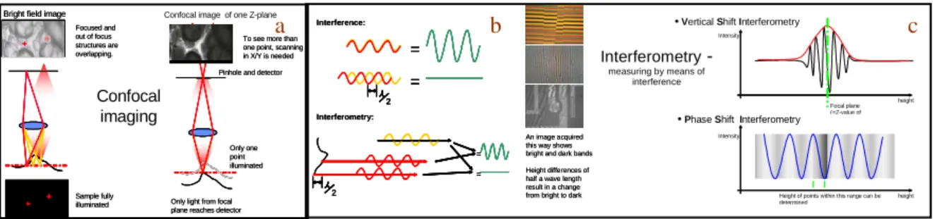
Confocal profilometers allow height measurement of surfaces with a wide range of textures (from very rough surfaces to very smooth ones) by scanning the sample vertically in steps so that each point on the surface passes through the focus. The height of the surface at each point is established by detecting the position of the maximum value of the axial response. Since only one or a very small number of points on the surface are illuminated simultaneously, an in-plane scan must be carried out in order to build up the axial response, i.e. the confocal image, in each vertical step for all the points falling within the field of view of the lens used (figure 1a).
The focus-detection instruments are gaining popularity due to their ability to carry out non-contact measurement over a wide measurement range with high resolution. Confocal scanning optical microscopes (CSOMs) use this focus detection technique. They were earlier used to measure the tomography of cells and tissues and two-dimensional profiles [3]. Since the early 1980s various three-dimensional measurement systems using this technique have been introduced [4].
In the confocal mode, the profilometer can carry out measurements with an extraordinary lateral resolution. This makes it possible to reduce spatial sampling to values of 0.15 µm for a conventional 150× lens, making it ideal for measurement of critical dimensions on the nanometric scale. In this mode, lenses with a large numerical aperture (NA) may be used, allowing measurement of polished surfaces with very high slopes (up to 70°). It is also possible to use lenses with super-large working distances (SLWD), allowing measurement of surfaces with high aspect ratio. In all cases, structured samples containing dissimilar materials can also be measured.
1.2. Interferometric Profilometry
The last few decades have witnessed major advances in interferometry [5]. We can look forward with confidence to an exciting future for this technique. The father of optical interferometry was undoubtedly Michelson. He was awarded the Nobel Prize in 1907 for ‘his precision optical instruments and the spectroscopic and metrological investigations conducted therewith’.
Optical interferometry (figure 1b) uses interference between light waves to make extremely accurate measurements. The two main working modes are phase shift interferometry (PSI), which allows measurement of the topography of very smooth surfaces with subnanometric resolution, and vertical scanning interferometry (VSI) with white light to measure the topography of smooth or moderately rough surfaces (figure 1c). The above mentioned PSI and VSI interferometers can carry out very fast measurements on the micrometric and nanometric scales. In addition, there is no intrinsic limitation in the vertical measurement range with the VSI technique. Nevertheless, both
MT.6
techniques have the drawback that they cannot easily deal with highly inclined smooth surfaces or with structured samples containing dissimilar materials.
Figure 1. (a) Confocal imaging composition, (b) Interferometry imaging composition and (c) PSI
and VSI interference formation. 2.
2. 2.
2. MethodologyMethodologyMethodology Methodology 2.1. System
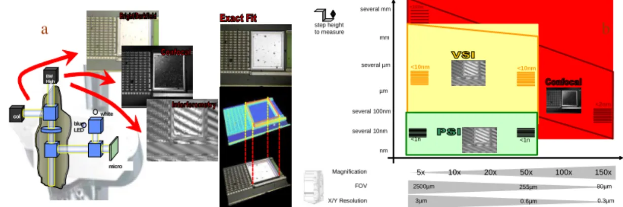
Dual (confocal and interferometric) technology optical profilometry (figure 2) provides a new optical surface metrology device for non-physical contact surface measurements that combines in one device the advantages of both techniques.
The system which is available at the Scientific and Technological Centers of the University of Barcelona (CCiTUB) comprises a light source including a light-emitting diode, beam splitters, a CCD (charge coupled device) and a number of interchangeable microscope lenses. These interchangeable microscope lenses comprise conventional lenses that may be used to obtain confocal images and interferometric lenses that may be used to obtain interferometric images. All this lenses are mounted on a rotating element that allows them to be changed easily, depending on the desired type of profilometer function.
The profilometer is provided with an illumination liquid crystal on silicon (LCOS) micro-display that allows the generation of a sequence of illumination patterns that provides, by means of application of the mentioned algorithms, confocal images, or allows total opening of all the illumination pixels to obtain interferometric images. The profilometer is completed with a polarising beam splitter associated with said micro-display.
Lastly, the profilometer includes a system to carry out the required vertical scanning of the sample so that all the points on the surface pass through the focus. This scanning is required for both PSI and VSI modes. The vertical scanning for measurement of the surface topography of the sample is carried out by means of a motor-driven vertical scanning system. The optical profilometer is completed with a system for positioning samples, comprising a motor-driven X-Y movement in the plane perpendicular to the optical axis of the profilometer. The profilometer software allows positioning of the area of the sample to be measured within the field of view of the lens in use by means of joysticks and also allows automatic topographic measurement of profiles or topographies extending beyond the field of view of the lens by means of the field stitching technique.
In the confocal mode, only one or a small number of points on the surface of the sample are illuminated simultaneously by the illumination pattern represented on the LCOS micro-display and the axial response for each of these points is calculated using the appropriate algorithm. In order to cover all the points on the surface to be measured, a series of illumination patterns must be projected onto that surface to obtain the value of the axial response for all the points falling within the field of view. In this way, the confocal image is obtained for a specific vertical position, where the corresponding value of the axial response for each point will be higher the closer it is to the position of the focus. Thus, confocal images provide very high contrast, since light is only perceived in the areas near the focus, while the areas at a distance from the focus appear as dark.
Confocal imaging
Bright field image Focused and out of focus structures are overlapping.
Pinhole and detector
Only light from focal plane reaches detector Confocal image of one Z-plane
To see more than one point, scanning in X/Y is needed Sample fully illuminated Only one point illuminated Confocal imaging
Bright field image Focused and out of focus structures are overlapping.
Pinhole and detector
Only light from focal plane reaches detector Confocal image of one Z-plane
To see more than one point, scanning in X/Y is needed Sample fully illuminated Only one point illuminated Interference: Interferometry: = = 2 = = 2 An image acquired this way shows bright and dark bands Height differences of half a wave length result in a change from bright to dark
Interference: Interferometry: = = 2 = = = = 2 2 2 = = 2 = = = = 2 2 2 An image acquired this way shows bright and dark bands Height differences of half a wave length result in a change from bright to dark
Intensity height Focal plane (=Z-value of Intensity height Height of points within this range can be determined
• Vertical Shift Interferometry
• Phase Shift Interferometry
Interferometry
-measuring by means of interference
MT.6
Measurement of the topography of a surface requires a sequence of confocal images in different planes of the sample located at different heights
Figure 2. (a) Dual (confocal and interferometric) scheme. Same optical path for all methods and
(b) comparison of technologies
In contrast with the confocal mode, the interferometric mode illuminates the whole surface to be analysed at once by means of a micro-display. In other words, in the interferometric mode, illumination patterns are not projected, but instead the whole surface is illuminated to obtain interferometric images for each plane of analysis. The beam emitted is passed through the splitter, which sends all the light to the surface of the sample and the image of the surface is projected onto the CCD device. The series of interferometric images resulting from the vertical scanning of the sample provides, by means of the appropriate algorithm, the surface topography of the sample being analysed. In this case a beam of light passes through a beam splitter. One part of the beam is sent to the surface of the sample and the other part is sent to a reference mirror. The light reflected from these surfaces is recombined and forms a pattern of interference fringes.
In this mode, the PSI technique may be used to measure continuous and very smooth surfaces with subnanometric vertical repeatability, regardless of the interferometric lens used, that is, for all values of numerical aperture. PSI devices allow users to carry out measurements of shape and texture even at scales lower than 0.1 nm. Nevertheless, they have the drawback of an extremely limited vertical measurement range. Likewise, the VSI technique may be used to measure either polished surfaces or rough surfaces with nanometric vertical repeatability for all values of numerical aperture. In addition, with the VSI technique the vertical measurement range is intrinsically unlimited and very high scanning speeds (up to 100 µm/s) may be used.
2.2. The performance of the system
2.2.1. The focus-spot dimension
The focus-spot dimension is an important factor, since it determines the spatial resolution (i.e. the smallest wavelengths which can be determined in the profile). The smallest spot which can be obtained is the so-called diffraction-limited spot, the size of which is determined by diffraction.
2.2.2. The depth response.
In a CSOM with point detection, the microscope image details are exactly at the focal plane. Thus, if a sample is vertically scanned through the focal plane, the photodetector receives the maximum amount of light when the surface is in focus. If the surface is in a lower or a higher position than the focus, the intensity of light gradually reduces to the background intensity. This response curve is referred to as the depth–response curve which is useful for optical sectioning of transparent samples and also during surface characterization using the intensity method. The depth response is dependent on the type of surface and the microscope objective. For determining the depth response, the microscope is initially aligned and the object surface is brought within the focusing range.
white blue LED BW High res col micro <100n m <2nm 10x 20x 50x 5x 100x 150x Magnification <10nm <10nm FOV 2500µm 255µm 80µm 0.3µm 3µm X/Y Resolution 0.6µm nm µm mm step height to measure several mm several µm several 100nm several 10nm <1n m <1n m a b
MT.6
2.2.3. The range resolution
The distance dz between half-power points (A and B) of the detector response (figure 3) is called the range resolution. For a reflection-type CSOM it is given by [6]
where θ is the half cone angle of the objective and it is equal to the numerical aperture of the objective.
The lateral resolution is determined by the size of the diffraction-limited focus spot.
Figure 3. The depth–response curve for a mirror surface
2.2.4. The selection of the objective
Many parameters influence the measurement results obtained with optical measuring systems. Factors such as the nature of the sensor, optical system, illumination, object and mechanical system influence the results [7].
2.2.5. Maximum allowable slope
The maximum allowable slope of the surface is determined as the angle at which the reflected light misses the microscope objective.
2.3. Components of surface topography
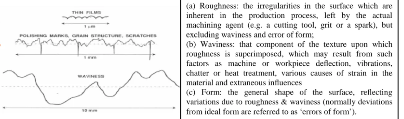
There are different components of surface topography generated by most common machining processes [8]. Surface roughness has two main attributes: roughness heights (or depths) and lateral dimensions. Figure 4 shows three types of surface features: (a) thin films, (b) polishing marks, grain structure and scratches and (c) waviness or orange peel.
Figure 4. Dimension of various types of surface features.
Surface structure can be divided into three general groups according to the lateral dimensions. Surface microroughness (often called roughness) has lengths up to approximately one millimeter and includes thin films, polishing marks, scratches and grain structure. Surface waviness, or mid-spatial-frequency roughness, has lengths from a few millimetres to perhaps one centimetre.
(a) Roughness: the irregularities in the surface which are inherent in the production process, left by the actual machining agent (e.g. a cutting tool, grit or a spark), but excluding waviness and error of form;
(b) Waviness: that component of the texture upon which roughness is superimposed, which may result from such factors as machine or workpiece deflection, vibrations, chatter or heat treatment, various causes of strain in the material and extraneous influences
(c) Form: the general shape of the surface, reflecting variations due to roughness & waviness (normally deviations from ideal form are referred to as ‘errors of form’).
a b
MT.6
Chemically-polished surfaces such as silicon wafers exhibit mid-spatial-frequency roughness, commonly called Orange peel. The overall surface shape often called the optical figure (departure from a perfect surface of the desired shape) or form in the machining industry, has lengths from the centimetre range to the size of the piece.
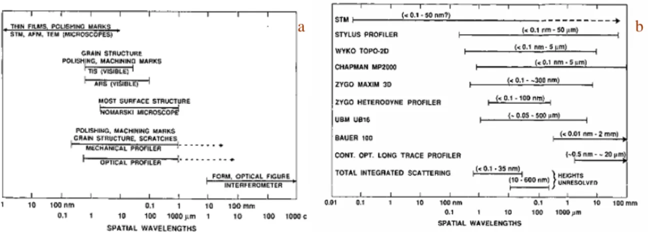
Although roughness values can be measured by a variety of techniques (figure 5) [9, 10], care should be taken when comparing measurements made with different instruments since the surface spatial wavelength ranges may be different. For example, Scanning Probe Microscopy (SPM) techniques are mainly used to better understand surface roughness on an atomic scale with a much better resolution than that of light microscopes. Therefore, SPM are the most long-scan profilers that have better lateral resolution and can measure surface heights in the waviness regime [11].
Figure 5. (a) Techniques for measuring surface roughness in various spatial wavelength regions
and (b) Schematic diagram of the characteristics of surface profilers and light-scatter measuring instruments. The horizontal bars give surface spatial wavelength ranges, and numbers in parentheses are the range of Rq heights that can be measured with each instrument (adapted from
[12]).
The surface data can then be analyzed to study the importance of surface texture in its relation to the surface performance. But the question is what features of the texture are important. Some features that appear as roughness in one application of a surface may well constitute waviness in another. Surface measurement is also limited by the resolution of the instrument used, as the real surface topography may be misrepresented owing to finite dimension of the stylus tip in stylus-based instruments [13-16].
Roughness of the structure is frequently measured and reported as a root-mean-square roughness (Rq) or, in precision machining, as an average roughness (Rz). For a three-dimensional
surface, Rq is calculated by including all surface heights from the reference plane. For an isotropic, Gaussian surface, it can be shown that Rq values given by a two-dimensional profile are the same
as given by a three-dimensional profile [17]. Typical units can be as small as angstroms or nanometers for the smoother surfaces and micrometers for rougher surfaces or lateral dimensions, called surface spatial wavelengths. Other roughness parameters are peak-to-valley distance (P-V) that is given by the distance between maximum peak or summit to minimum valley, peak-to-mean distance (Rp) that is the distance between maximum peak or summit and mean line (for a
two-dimensional profile, the peak is defined as a point higher than its two adjacent points; for a three-dimensional profile, the summit is defined as a point higher than its four adjacent points and a valley is defined in the same way as a peak or a summit but in a reversed order) and correlation length (β) is a spatial parameter giving information about how surface heights are oriented in space.
MT.6
2.3.1. Effect of scan size
It is commonly observed that the roughness parameters of engineered surfaces change with scan size. In particular, Rq and β generally increase with scan size. It is due to longer and longer wavelength features included in the image as the scan size is increased [18-19].
2.3.2. Selection of scan size
The selection of scan size and sampling interval can change the roughness parameters Rq, Rp, P-V and β. The question is: which is the suitable scan size and sampling interval?
In practice, the scan size should be related to the bandwidth covered by the nominal contact width of the physical problem involved. If a surface contains a broad bandwidth of wavelengths up to or longer than the contact width, then the scan size should be chosen as the contact width. On the other hand, if a surface contains a long-wavelength limit smaller than the contact width, then the scan size can be set equal to the long- wavelength limit.
2.3.3. The selection of the objective.
Also the roughness measurements are affected by the use of a low-NA objective because of an increase in the spot size which determines the spatial resolution. It can also be seen that the depth– response curve broadens as the surface roughness increases. Hence the response curve can give information about the surface roughness. The full-width-at-half-maximum characteristic of the response curve can be correlated to the surface roughness. The shape of this curve also indicates the glossy nature of the surface.
3. 3. 3.
3. ApplicationsApplicationsApplications Applications
There are countless applications (figure 7) that require knowledge of the topography of the surface of an object and thus determination of its microscopic shape. Such analysis may, for example, form part of a quality control process. Functional characterization was carried out for some industrial applications [20]. Several researchers have also worked on the characterization of surfaces in three-dimensions using various instruments and techniques [21–23].
The optical profilometer is extremely versatile for carrying out accurate measurements of the shape and texture of all types of surfaces on the micrometric and nanometric scales, including structured or stratified samples containing dissimilar materials.
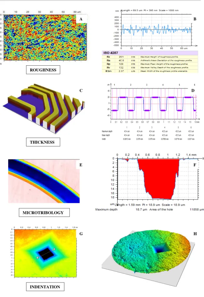
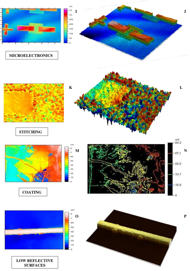
Optics in general played an important role in measurement and, with the advent of opto-mechatronics; it is once again at the forefront of measurement [24]. There are many applications in which the optical profiler may be used. By way of example, the profiler may be used for the measurement of high-aspect ratio surfaces such as those containing grooves, holes or indentations (figure 7g-h), the steeply sloped polished surfaces present in optical structures as micro-lenses and micro-prisms or on-Si micro-finished surfaces, noticeably rough and not very reflective surfaces such as paper (figure 7o-p) or also surfaces of very low roughness containing dissimilar materials such as optical or electronic microdevices (figure 7i-j), surfaces exhibiting different textures and relatively large sized surfaces such as a mould, a coin or a wafer, which can be measured with the option of field stitching (figure 7k-l), etc.
Surface topography plays an important role in understanding the nature of sliding surfaces. No matter how finely finished, most machinery rubbing surfaces are rough from a microscopic viewpoint. As a result, the microtopography of a single surface and the nature of a contact between two surfaces form an essential background for developing a fundamental concept of the nature of two sliding surfaces.
On the other hand, roughness and form must be studied to determine the functional performance of engineering parts. The measurement and understanding of surface topography is rapidly attracting the attention of physicists, biologists and chemists as well as engineers.
The main emphasis in surface-related research is on the determination of parameters that characterize surface properties, mainly those which are correlated to surface-formation mechanisms and surface behaviour in a fundamental way [12]. Monitoring the texture has been a simple way of
MT.6
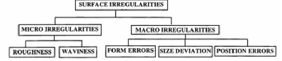
controlling the manufacturing process. Measurement of surface topography falls within the field of quality control and product optimization. As we previously remarked, the surface-topographical aspects which influence product performances are roughness, waviness, form, lay, laps, tears and micro-cracks (figure 7a-b). The surface irregularities are broadly classified into micro and macro as shown in figure 6. Surface topography is important from the point of view of such fundamental problems as tribology (figure 7e-f), friction, contact, lubrication, wear, fatigue strength, tightness of joints, conduction of heat and electrical current, cleanliness, reflectivity, sealing, positional accuracy, load-carrying capacity, resistance to corrosion and adhesion of paint and coatings [24]
Figure 6. Types of surface irregularities
Some of the current applications of optical interferometry include measurements of distances (figure 7c-d), displacements and vibrations, tests of optical components and systems, studies of surface structure, studies of fluid flows, measurements of temperature, pressure, electrical and magnetic fields, rotation sensing and high-resolution stellar imaging.
Surface roughness [25] is becoming increasingly important for applications in many fields. In optics, low scatter lenses, mirrors, filters, beam splitters and other optical components. In the field of microelectronics, as line widths and circuit elements become smaller and shorter wavelengths are used to produce higher density microcircuits on silicon wafers, the wafer surfaces have to be smoother and less wavy. Disks require surfaces whose roughness properties are carefully controlled and finally, the characterization of stratified media such as semiconductors, flat panel displays, optical coatings (figure 7m-n) and medical devices involves measuring the thickness and optical constants of thin layers with high lateral and vertical resolutions.
In conclusion, the obvious advantage of any optical profiler is that, since it is non- contact, it cannot damage the surface. Also, optical profilers are user friendly, measurements can be carried out easily and rapidly, and data reduction is rapid. The main disadvantages of optical profilers are (a) their lateral resolutions are limited by the properties of the optical systems and by the light beams illuminating the surfaces, (b) they cannot distinguish between changes in topography and changes in optical constants on the surface since they are sensitive to the phase of the light reflected from the surface, (c) the maximum step height that can be measured is less than half of the incident wavelength.
MT.6 ROUGHNESS THICKNESS MICROTRIBOLOGY INDENTATION A B C D E F G H
Figure 7a. Images of different applications of Optical Profilometers (a-b) roughness,
MT.6 MICROELECTRONICS STITCHING COATING LOW REFLECTIVE SURFACES I J K L M N O P
Figure 7b. Images of different applications of Optical Profilometers (i-j)
microelectronics, (k-l) stitching, (m-n) coatings and (o-p) low reflective surfaces. K
MT.6
Acknowle AcknowleAcknowle
Acknowledddgmentsdgmentsgmentsgments
The authors would like to thank Dr. J.J. Jaramillo, Dra. Monica Martínez, Dr. Albert Romano, Dra. Núria Cinca and Adriana Velásquez for the reproduction of unpublished results.
References ReferencesReferences References
[1] Patent US7636167 B2
[2] Sherrington I and Smith E H 1988 Modern measurement techniques in surface metrology: part II—optical instruments Wear 125 289–308
[3] Gordon S K and Timothy R C 1989 Confocal scanning optical microscopy Phys. Today September 55–62
[4] Migot J and Gorecki C 1983 Measurement of surface roughness: comparison between a defect-of-focus optical technique and the classical stylus technique Wear 87, 39–49. [5] P Hariharan .Rep. Prog. Phys. 54 (1990) 339-390.
[6] Gordon S K and Timothy R C 1989 Confocal scanning optical microscopy Phys. Today September 55–62.
[7] De Chiffre L and Hansen H N 1995 Metrological limitations of optical probing techniques for dimensional measurements Ann. CIRP 44 501–4.
[8] Dagnall H 1986 Exploring Surface Texture (Leicester: Rank Taylor Hobson)
[9] De Chiffre L and Nielsen H S 1987 A digital system for surface roughness analysis of plane and cylindrical parts Prec. Engng 9 59–64.
[10] Carneiro K, Jensen C P, Jorgensen J F and Garnoes J 1995 Roughness parameters of surfaces by atomic force microscopy Ann. CIRP 44 517–20.
[11] ref. Handbook SPM
[12] Stout K J (ed) 1994 Three dimensional surface topography. Measurement Interpretations and Applications.
[13] D.J. Whitehouse, Handbook of Su$ace Metrology, Institute of Physics Bristol, 1994. [14] T.R. Thomas (ed.), Rough Surfaces, Longman, London, 1982.
[15] D.J. Whitehouse and J.F. Archard, The properties of random surfaces of significance in their contact, Proc. R. Sot. London, Ser. A, 316 (1970). 97-121.
[16] D.J. Whitehouse, Theoretical analysis of stylus integration, Ann. CIRP, 23 (1974) 181-182. [17] R.D. Gibson, The surface as a random process, in T.R. Thomas (ed.), Rough Swjaces,
Longman, London, 1982.
[18] R. Sayles and T.R. Thomas, Surface topography as a nonstationary random process, Nafure (London), 271 (1978) 431-434.
[19] Chin Y. Poon, Bharat Bhushan Wear 190 1995) 76-88
[20] De Chiffre L, Christiansen S and Skade S 1994 Advantages and industrial applications of three dimensional surface roughness analysis Ann. CIRP 43 473–8.
[21] Boudreau B D and Raja J 1992 Analysis of lay characteristics of three-dimensional surface maps Int. J. Machine Tools Manufact. 32 171–7.
[22] Ganesha Udupa, M Singaperumal, R S Sirohi andM P Kothiyal. Meas. Sci. Technol. 11 (2000) 305–314
[23] Bennett J M and Mattson L 1989 Introduction 10 Surface Roughness and Scattering (Washington. DC: Optical Society of America)
[24] Bennett J M 1992 Surface Finish and Its Measurement (Washington, DC Optical Society of America)