Università degli Studi di Catania
Dottorato di Ricerca in Scienza
dei Materiali XXV Ciclo
2009-2012
Università degli Studi di Catania
New Strategies for the
Synthesis of 2D
Nanomaterials
Marco Giovanni Sinatra
Tutor:
Chiar.mo Prof. G. Compagnini
Coordinatore:
Chiar.mo Prof. A. Licciardello
Dottorato di Ricerca in Scienza
dei Materiali XXV Ciclo
New Strategies for the
Synthesis of 2D
Nanomaterials
Marco Giovanni Sinatra
Chiar.mo Prof. G. Compagnini
CONTENTS
Table of Contents...3
Introduction...5
1. Synthesis and properties of two dimensional nanomaterials and related structures: state of the art...13
1.1 Molybdenum disulphide nanomaterials...14
1.1.1. MoS2 fullerene-like...15
1.1.2. MoS2 monolayers...22
1.2. Carbon based nanomaterials...29
1.2.1. Carbon nanowalls………..… 30
1.3. Conductive nano-network………..….….……...37
1.3.1. MoSI functionalized with gold nanoparticles...38
References...42
2. Synthesis and characterization of MoS2 nanostructures...45
2.1. MoS2 fullerene-like...47
2.2. MoS2 layered materials...74
3. Synthesis and characterization of Carbon Nanowalls...93
References...107
4. Synthesis and characterization of two dimensional hybrid systems MoSI+Au...109
References...130
5. Conclusion...131
6. Future Work Functionalization of CNWs with Ag...133
INTRODUCTION
In the past decade, the interest in nanoscale materials had an enormous impact and industrial potential deriving from the fact that new properties are acquired at this length scale and also these properties change whit their size or shape. Future progress could change our advances to assembling, communications technology and electronics, making previous technology redundant and leading to applications which could not have been developed or even thought about, without this new approach.
A nanostructured material is defined as a solid material characterized by at least one dimension in the nanometer range. Size effects establish an exceptional and intriguing aspect of nanomaterials.
The effects determined by size are part of the evolution of structural, electronic, electromagnetic, spectroscopic, thermodynamic and chemical features of these restricted systems with changing size. The properties of a material are based on the type of movement its electrons can perform, which depends on the space available for them. Therefore, the properties of a material are identified by a specific “length scale”, commonly on the nanometer dimension. If the physical size of the material is decreased below this length scale, its properties change and become sensitive to size and shape. In any material, considerable modification of intrinsic optical and electrical properties with decreased size will be noticed when the energy spacing between the electronic levels is superior to the thermal energy (kT). For instance, in the bulk material, the electronic energy levels are continuous while in nanomaterials are discrete (finite density of states), and this behavior is due to the confinement of the electronic wave function to the physical dimensions of the particles.This phenomenon is called quantum confinement and therefore nanocrystals are also referred to as quantum dots (QDs). Moreover, nanocrystals presents a high surface area and a large percentage of the atoms in this material is on its surface. Since this percentage depends considerably on the size of the particle, it can give rise to size effects in physical and chemical properties of this material.
When we talk about nanomaterials we indicate a substance with an extreme small size, at least one dimension 100 nm or less. Nanomaterials can be classified in zero dimensional as quantum dots, one dimensional as MoSI nanowires or polyynes, two dimensional, as MoS2 sheets or carbon nanowalls, or three dimensional as metallic colloids.
Figure 2. Classification of Nanomaterials (a) 0D spheres and clusters, (b) 1D nanofibers, wires, and rods, (c) 2D films, plates, and networks, (d) 3D nanomaterials.
These materials have aroused a high interest in the last years by advantage of their singular electrical, optical, mechanical and magnetic properties. Following will be shown some examples of these nanomaterials:
For instance, nanophase ceramics are very interesting because they are more ductile at elevated temperatures as compared to the coarse-grained ceramics. Another example is nanostructured semiconductors. These materials present various non-linear optical properties and can be used as windows layers in solar cells. Semiconductor Q-particles also exhibit quantum confinement effects which may cause to particular properties, for instance silicon germanium quantum dots as infrared optoelectronic devices and the photoluminescence in MoS2 monolayers deposited on silicon substrate.
Nanostructured metal colloids could play a fundamental role in catalytic applications. Their substantial advantages are about activity, selectivity and lifetime in chemical transformations and electrocatalysis (fuel cells). Enantioselective catalysis was also achieved using chiral modifiers on the surface of nanoscale metal particles [2].
In literature many different kind of synthesis are present. In particular the science community adopted two different approaches to produce nanomaterials, top-down and bottom up methods.
Figure 3. Outline of top down/bottom up approaches
In figure 3 I reported the outline of top down bottom up approaches. In practice, these two methods may be considered as a different ways of thinking. In particular top-down is estimated as a mode of analysis or decomposition, while bottom-up is considered as a kind of synthesis. A top-down approach is fundamentally the breaking down of a system, commonly called bulk material, to obtain information about the system composition. With this method we can define an overview of the system, acquiring specific details about first-level subsystems. After that, each subsystem is analyzed in greater detail until the entire bulk material is reduced to base elements. One of the most important example of this approach is represented by the scotch tape exfoliation of graphene.
It consists in a piling off of graphite in order to reduce its thickness and split graphite crystals into increasingly thinner pieces to produce graphene’s layers. [3] A bottom-up approach is the assembling together of the base elements, usually called building blocks, to create the nanostructure. The nanomaterial features shall be laid before the synthesis and in this way we can lead the growth in order to obtain a particular nanostructure with a specific property. The synthesis by laser ablation in liquid, for instance, is an example of this type of approach. It consists by irradiating a solid target submerged in a liquid with a laser beam. During this phenomena it’s generated a plasma in which there are some reactive species. The interaction of these species with each other forms some new nanomaterial. For instance metal colloids are produced by laser ablation in water. [4]
In this thesis I’m going to report the obtained results during my PhD experience. I was able to synthesize some kinds of 2D nanomaterials by using new strategies for their synthesis. In particular I used pulsed laser ablation in liquid (PLAL) to synthesize nanostructures made of MoS2 with a particular structure fullerene-like and I produced MoS2 few-layers materials by applying mechanical exfoliation of MoS2 powder assisted by ultrasonic treatments. Using PLAL and applying an electric field after the synthesis process I was able to produce a new and interesting carbon-based nanostructure called Carbon Nanowalls (CNWs) made of vertically oriented graphene sheets on a substrate. I have also produced a hybrid 2D composite by mixing MoSI nanowires with gold nanoparticles and I have studied the chemical bonding state of this interaction by using
of X-Ray Photoelectron Spectroscopy (XPS). Moreover I have studied the spectroscopy, morphology and chemical bonding features of all nanostructures obtained. I used following techniques as Raman spectroscopy, UV-VIS spectroscopy, Atomic Force Microscopy (AFM), Scanning/Transmission Electron Microscopy (SEM/TEM) and the aforementioned XPS.
During the next chapter, I’m going to describe the standard synthesis methods and the main properties and application of 2D nanostructures, which I have studied during my experience, and after that I’m going to show you my experimental work and my experimental results.
1 SYNTHESIS AND
PROPERTIES OF TWO
DIMENSIONAL
NANOMATERIALS AND
RELATED STRUCTURES: STATE
OF THE ART
As said before, during my PhD experience, I focused my attention on the new strategies for the synthesis of 2D nanomaterials in order to improve the standard synthesis routes. Indeed, usually, to create a nanostructure we need, or to work under vacuum and at high temperature or to employ some reactants which we have to remove after the synthesis. In this chapter I’m going to show you some different standard synthesis routes to produce nanomaterials as MoS2 fullerene-like or carbon nanowalls. First I’m going to analyze synthesis properties and application of molybdenum disulphide nanomaterials after that I will discuss the case of carbon nanowalls and in the end of this chapter I will focus my attention on the manufacturing of conductive nano-network made of MoSI functionalized with gold nanoparticles.
1.1 MOLYBDENUM DISULPHIDE NANOMATERIALS
The dimension of an object is one of the most important material parameters; the same chemical compound could manifest impressively different properties depending on if it is organized in a 0D, 1D, 2D, or 3D crystal structure. Materials with layered structures continue a broadly studied topic in actual chemistry and physics. Most of the auspicious technological applications even though attend to intercalation compounds of layers materials. The transition metal dichalcogenides manifest appreciable multiplicity in their physical properties, from the fields of metals, to semiconductors, insulator and superconductors. A significant characteristic of these materials is that they crystallize in a quasi two-dimensional type of layered structurethat gives considerable anisotropy to many of their properties. In addition, the layered structure of MoS2 is very similar to graphite structure. This particular aspect allows to synthesize fullerene-like structures and nanotubes from inorganic compounds with a crystal structure akin to graphite.
Nanoparticles of compounds with a layered structure go under the large surface energy correlated with the external atoms and fold into hollow cage-like structures. To get over the large elastic energy associated with the folding process, considerable activation energy must be supported for the process to take place, otherwise the reaction is very slow.[5]
1.1.1 MoS
2The fullerenes
because they presents topologies. The molecule (see Figure the external sp
atoms into the hexagonal network structure of graphite bending and strain into the structure.
Figure 4. Schematic cases the surface energy,
2
FULLERENE-LIKE
he fullerenes, among nanophase materials, take up a special place, they presents high symmetry and have an unique hollow topologies. The predisposition of graphite nanoclusters to form the C molecule (see Figure 4) has been ascribed to the large surface energy of
al sp2 bonded carbon atoms. Adding rings composed to into the hexagonal network structure of graphite
bending and strain into the structure.
. Schematic structures of graphite and MoS2 nanoclusters. Note that in both
cases the surface energy, that weakens the planar topology of the concentrated in the edge planes parallel to the c-axis (
a special place, first unique hollow-cage of graphite nanoclusters to form the C60 ed to the large surface energy of rings composed to five into the hexagonal network structure of graphite it’s induced
nanoclusters. Note that in both s the planar topology of the structure, is
The great stability of the C60 molecule (Figure 5) was attributed to the fact that this is the smallest carbon cluster with twelve disjoint pentagons [6].
Figure 5. Schematic structures of the C60 molecule
Earlier than the discovery of the C60 molecule, Iijima et al. [7] proposed that carbon “onions” (see Figure 6A) are composed of various carbon cages, each with 12 pentagonal rings disposed in the carbon hexagonal (graphite) network.
Figure 6. Transmission Electron images of (A) carbon fullerene and (B) MoS2
fullerene-like
Similarly to graphite, layered compounds like MoS2, do not exhibit dangling bonds on the basal (0001) plane (⊥c), that establishes itself with very inert and low energy (0001) surface (Figure 4). On the contrary, the
dangling bonds of the prismatic face perpendicular to the basal plane (|| c), are very reactive. Therefore, nanoclusters of 2-D materials have high percentage of their atoms on the prismatic edges with unsaturated bonds and this aspect gives them an instability in the planar structure. Accordingly, these materials form hollow-cage nanostructures without dangling bonds. This analogy between carbon and 2-D (layered) compounds was indicated first for WS2 nanoclusters [8] and later for MoS2 [9-10-11].
These materials are very important for their interesting properties. For instance MoS2 is one of the most important solid lubricants and this characteristic is enhanced by the nanosize [12].
It’s possible to notice in the figure 7 that the friction coefficient of a commercial oil (PAO) with or without the additive is different. In particular by comparing the behavior of PAO with MoS2 as bulk material and MoS2 as fullerene.like (IF MoS2), we can notice that the friction coefficient is better in the case of PAO with IF MoS2.
In analogy to carbon fullerenes, the main reason of the formation of hollow cage structures of these compounds is due to the dangling bonds on the prismatic face (|| c) of the metal dichalcogenide (MX2) nanocluster (Figure 5). The deflections from planarity of the nanocluster during the formation of a hollow cage structure is due to the elastic strain involved in tilting the chemical bonds.Therefore, a source of energy input increase the yield of the synthesis of inorganic fullerenes [13]. Different kinds of synthesis were adopted for the formation of hollow closed structures from layered compounds. It’s possible to divide into two kinds of procedures: (a) synthetic procedures that arise far from equilibrium, and (b) synthetic procedures that are near to equilibrium conditions.The most commonly synthesis used to production these materials is not very different from the gas-phase reaction. This method is a progressively sulphurization of MoO3 in gas phase [5]. The procedure is described by Tenne et al. in one of their more relevant work: “Molybdenum oxide is volatile under reducing conditions >700 °C, and hence a gas-phase reaction was adopted for the synthesis of IF-MoS2. Typically, a 30-mg portion of MoO3 powder (>99% pure) is heated (>800 °C) and is slowly reduced to MoO3-x by a stream of forming gas (typically 5%H2/95%N2). The suboxide sublimes and effuses out of a nozzle where it crosses a
stream of H2S gas mixed with a forming gas. The reaction products are collected on a quartz scepter, which is positioned 3 cm away from the crossing point of the two gas streams and is maintained at the same temperature (>800 °C). The
converted into nested IF polyhedra within 30 min of firing time. The average size of the oxide nanoparticle and the ensuing IF
with temperature. It was found that at >900 °C, platelets with the 2H MoS2 structure abound and become the sole product at >950 °C.
Figure 8. Scheme of the growth model of the inorganic fullerene
The growth mechanism reported in Figure 8. In the first oxide nanoparticle reacts with H a complete sulfide shell composed absorbing the entire oxide nanoparticle.
nanoparticle from its nearest neighbors thereby prohibiting coalescence with a forming gas. The reaction products are collected on a quartz scepter, which is positioned 3 cm away from the crossing point of the two gas streams and is maintained at the same temperature (>800 °C). The collected nanoparticles are progressively converted into nested IF polyhedra within 30 min of firing time. The average size of the oxide nanoparticle and the ensuing IF-MoS2 increases with temperature. It was found that at >900 °C, platelets with the 2H
structure abound and become the sole product at >950 °C.”
the growth model of the inorganic fullerene-like from oxide nanoparticles.
The growth mechanism of quasi-spherical nested nanoparticles is . In the first moment of the reaction, the molybdenum oxide nanoparticle reacts with H2S gas, which conducts to the growth of composed of one or two MoS2 atomic layers ing the entire oxide nanoparticle. This sulfide shell isolates the nanoparticle from its nearest neighbors thereby prohibiting coalescence with a forming gas. The reaction products are collected on a quartz scepter, which is positioned 3 cm away from the crossing point of the two gas streams and is maintained at the same collected nanoparticles are progressively converted into nested IF polyhedra within 30 min of firing time. The increases with temperature. It was found that at >900 °C, platelets with the
2H-spherical nested nanoparticles is molybdenum s to the growth of atomic layers lates the nanoparticle from its nearest neighbors thereby prohibiting coalescence
of the nanoparticles, which would lead to the formation of 2H-MS2 platelets. Within more or less a minute, hydrogen diffusion into the nanoparticles (and oxygen out diffusion) allows to reduction of the oxide core and permits the formation of crystallographic plans. In the second part of the reaction, which can carry on 120 min and even more, sulfur diffuses slowly into the core of the nanoparticle and slowly converts the sub-oxide into sulfide, which becomes hollow at the end of the process. This synthesis actually consists of two independent processes. The rapid radial diffusion of sulfur atoms inward through dislocation at the outer MoS2 layers and the slow diffusion of the sulfur atoms along the layers into the single-growth front of the sulfide. This process provides a continuous MoS2 shell that grows inward into the oxide core.
The main problem of this synthesis is the need to work under vacuum with high temperature and, primarily, the presence of dangerous gas reagents like H2S and H2. For this reason I decided to develop a new synthesis route, for MoS2 fullerene-like, in order to work in a safer, cheaper and faster way by using the PLAL.
1.1.2 MoS
2MONOLAYERS
Another important bi-dimensional nanostructure of MoS2 is represented by mono-layer material. Recent developments in synthesis of ultrathin layered materials in monolayer thickness have allowed examinations of new low-dimensional physics, as demonstrated by massless Dirac fermions and anomalous quantum Hall effects observed in monolayer graphene [14].Layered transition metal dichalcogenides, like MoS2, are another kind of materials, in which the interactions of the d-electrons’ can produce to new physical phenomena. This material is composed of covalently bonded S-Mo-S sheets that interact each other by weak van der Waals forces. Molybdenum disulphide, like bulk material, is a semiconductor with an indirect bandgap of about 1eV and it has been employed for photocatalytic and photovoltaic applications due the high absorption in the solar spectrum region. Optical properties and quantum confinement effects on the electronic structure of MoS2 have well known and noticed in MoS2 thin films as well as in MoS2 nanoplates and nanotubes [15].In particular Splendiani et al. [16] report the emergence of photoluminescence in ultrathin layers of MoS2. They founded that MoS2 photoluminescence, increased with decreasing layer thickness, and that luminescence from a monolayer was the strongest while it was absent in bulk material.The cause of this luminescence behavior is due to the fact that MoS2 change into a direct bandgap semiconductor when thinned to a monolayer.
Figure 9. Photoluminescence and Raman spectra of MoS2 monolayer, bilayer,
In Figure 9a, it’s reported photoluminescence spectra from monolayer, bilayer, hexalayer, and bulk MoS2. In bulk MoS2, no photoluminescence is present while for MoS2 monolayers the Raman and photoluminescence intensities show a dependence from the layer: MoS2 Raman signal is weaker in the monolayer MoS2, due to lower quantity of material, than in the bulk material, while photoluminescence is higher regardless of the reduced amount of material. For this reasons MoS2 monolayer photoluminescence is due to an intrinsic material property while the luminescence resonances is attributable to the direct excitonic transitions. For this reason the exfoliation methods, to produce two dimensional crystals, whose present interesting properties for different application like energy storage and electronics, are under investigation. These exfoliations can be divided in two different approaches: first mechanical method, like for instance scotch tape, that produces a small amount of layers, as reported in the figure 10[17]
Figure 10. Scanning electron and atomic force images of 2D crystal matter
and second liquid-phase exfoliation methods would allow the formation of higher amount of material and the production of novel hybrid and composite materials [18].
Coleman et al. have exfoliated different kinds of two dimensional materials in a novel liquid-phase method using different common solvents. First they dispersed bulk material in a solvent by sonication and after that they centrifugated the sample in order to remove the bulk
materials from the dispersed one. Some of the more promising solvents were Nmethyl-pyrrolidone (NMP) and isopropanol (IPA) and the improvement of the exfoliation procedure gave concentrations as high as 0.3 mg/ml for MoS2. This method allowed to prepare films of BN, MoS2, and WS2 by vacuum filtration or spraying, with thickness ranging from a few nanometers to hundreds of micrometers. To verified what they produced Coleman et al. made different kinds of analysis reported in figure 11. They used scanning electron and helium ion microscopy of the surface and edges of these films (Fig. 11, B and C).
They illustrated this by preparing hybrid dispersions and so films of MoS2 or WS2 mixed with graphene or single-walled nanotubes (SWNTs) (Fig. 11, D and E).
I decided to perform the same procedure to exfoliate MoS2 but I tried to change solvent by the using of water and a surfactant. It was necessary to prevent the re-aggregation of the layer after the sonication. Furthermore I employed the centrifugation procedure to maximize the process yield.
1.2 CARBON BASED NANOMATERIALS
The discovery of graphene has stimulated enormous interest on 2D carbon nanostructure in view of their extraordinary properties and potential applications [19]. A challenge has always been to identify a high yield production pathway, suitable to give graphene or graphene-like structures without collateral structural damage and with the possibility to manipulate the layers (individually or collectively) in order to have a particular arrangement and position for given applications [20]. Alternative to single layer graphenes, the so called carbon nanowalls (CNWs) have been discovered and investigated [21]. They consist of aligned graphene sheets standing on a substrate with large surface areas and sharp edges. For these reasons they are expected to be good catalyst support structures for fuel cells as well as electron field emitters for lithium ion batteries. So far, research groups have explored different synthesis methods of CNWs essentially based on plasma-enhanced chemical vapour deposition approaches [22].
1.2.1 CARBON NANOWALLS:
The first paper, on the preparation of two-dimensional carbon nanostructures, was wrote more than 10 years. Ando et al. [23] found something like “carbon roses” during the synthesis of carbon nanotubes in 1997. In 2002, Wu et al. [24] reported the formation of two-dimensional carbon nanostructures, “carbon nanowalls,” growing vertically on catalyzed substrates. In figure 12 [25]it’s reported a scheme of Carbon nanowalls structures in order to give an understanding of the organization of the layers.
Figure 12. Schematic structure of Carbon Nanowalls grown on a substrate
This material shows a very interesting properties in many field like field emission, catalysis and electrochemical applications. For instance CNWs decorated with Pt nanoparticles have shown good electrocatalytic properties as reported in the work of Giorgi et al. [26]. They noticed that enhanced activity for methanol oxidation was not linked to the increase of platinum load and specific surface area, but rather it was depended from the microstructure of the Pt cluster at level of nanoparticles (<10 nm). The carbon nanowalls structures acted as a good substrate for Pt electrocatalyst for methanol oxidation with a remarkable enhancement respect to the state of art carbon powder.
Another important application of these systems is the formation of 3D field emission array as reported by Stratakis et al. [27]. They noticed that the field emission performance and long-term stability of the CNWs structures is more superior to that of planar carbon nanowall mats and comparable to that reported for optimized carbon nanotube based emitters.
Carbon nanowalls usually have been grown using various CVD methods such as microwave plasma, radio frequency (RF) inductively coupled plasma [28], and even by sputtering of a glassy carbon target. This synthesis methods are the same procedure used to prepare diamond films and carbon nanotubes.Commonly, a combine of hydrocarbon (CH4) and hydrogen, is used as precursor gases for the preparation of carbon nanowalls. High-density plasmas like inductively coupled plasma and microwave plasma are applicable for the synthesis of CNWs because they present a good behavior in the decomposing H2 molecules. This
phenomena it’s very important in the formation of CNWs because it is considered that a large amount of H atoms is required for the growth of the nanostructures, which is similar to the case for diamond growth.The growth of CNWs doesn’t require metal catalysts like other carbon nanostructures (carbon nanotubes). Consequently, carbon nanowalls have been fabricated on several substrates, including Si, at substrate temperatures of 500–700°C without the use of catalysts [29].
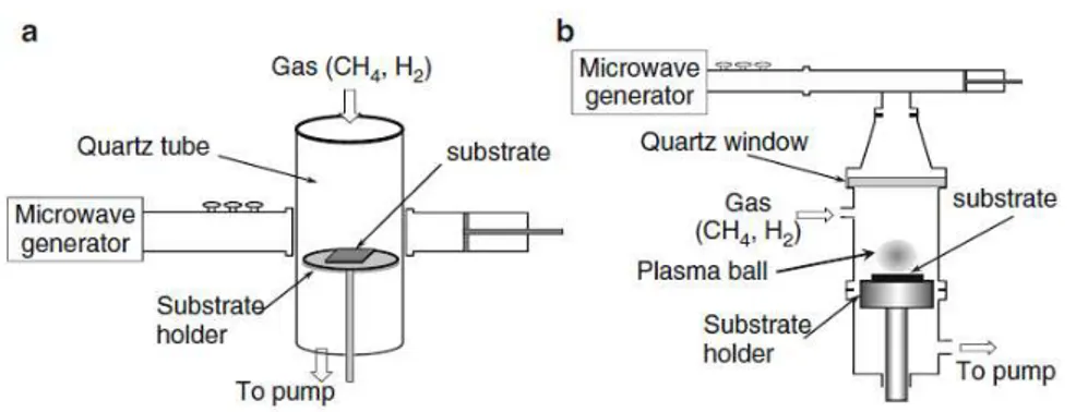
Figure 13 a, b show two types of microwave plasma-enhanced chemical vapor deposition (MWPCVD). In particular fig. 13 a show the NIRIM apparatus (the National Institute of Research of Inorganic Materials, Japan) while in fig. 13b it’s reported ASTeX scheme (Applied Science and Technology, Inc.).In the case of NIRIM-type MWPCVD system, the CH4/H2 plasma is generated in a cylindrical quartz tube, which meets a rectangular waveguide, fig 13a. The most important advantages of NIRIM-type reactors are (1) easy reactor design with low set-up costs and (2) possibility to vary the position of substrate respect to the plasma. On the other hand, the diameter of the cylindrical quartz tube limited the size of substrate to approximately a few cm2. The ASTex-type reactor consists of a cylindrical stainless steel chamber. Above the substrate there is a discharge called a “plasma ball”. In this system, the CVD process could be operated at high pressures (~103 Pa), but it's impossible to vary independently the reactor pressure and microwave power. At too high pressure or low microwave power, plasma cannot be sustained.
Figure 13. Schematic of microwave plasma-enhanced CVD systems. (a) NIRIM (National Institute of Research of Inorganic Materials) type, (b) ASTeX (Applied
Science and Technology, Inc.) type
Wu et al. reported the synthesis of carbon nanowalls on the catalyzed substrate using the NIRIM-type MWPCVD reactor [24].
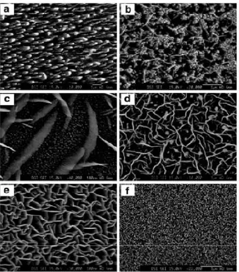
For the first time carbon nanowalls was synthesized during the growth of carbon nanotubes; but now Wu et al. successfully synthesized carbon nanowalls on various substrates using MWPCVD, and analyzed the formation of carbon nanowalls with different gas flow rate ratio and electrical field. Typical carbon nanowalls were grown employing a mixture of H2 and CH4 in the flow rate ratio of 4 and substrate temperatures of 650–700C. In figure 14 are reported SEM images of carbon nanostructures grown at different H2/CH4 flow rate ratios. This parameter causes many changes to the morphology of the nanocarbon films. Typical carbon nanowall film was grown at the H2/CH4 flow rate ratio of 4, as shown in Fig. 14 e.
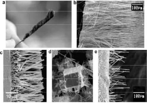
Chuang et al., using a source mixture made of ammonia and acetylene, reported the growth of carbon nanowalls in 3D aggregates by MWPCVD using ASTex-type reactor.They also studied field emission properties of this structures [30].
Figure 14. SEM images of carbon nanostructures grown at different H2/CH4 flow rate
The gas flow rate ratio NH3/C2H2 below 1 allows to create microstructures of carbon nanowalls. In their method, growth of carbon nanowalls was catalyst-free. Similar structures obtained with this technique are reported in Fig. 15.
Figure 15. SEM images of carbon nanowalls grown by MWPCVD using ASTex-type reactor
All of the techniques reported above need to high temperature to work and also they need to gas flows that means it’s obliged to use complicated vacuum systems. For these reasons we tried to obtained CNWs in a way without the necessity to employ vacuum systems or high temperature. We obtained CNWs by using PLAL and after that we applied an electric field in order to start the growth of nanostructures onto the electrodes.
1.3 CONDUCTIVE NANO-NETWORK
The fast development of nanotechnology has conducted to requests on new 1D materials with new functional properties. Carbon nanotubes have obtained most attention, followed by nanowires of very different kinds. In the last years inorganic molecular wires, in particular molybdenum halide, have appeared as a new type of 1D materials with conspicuous molecular-scale functionality. These molecular nanowires are single in terms of molecular properties and structure. Their one-dimensional polymer structure gives rise to some very unusual physical properties. Anionic bridges which engage Mo clusters together into one-dimensional chains are exceptionally strong, yet highly deformable, giving rise to extraordinarily high Young’s moduli and nonlinear mechanical properties respectively.The sulfur atoms within the structure facilitate diverse functionalization chemistry to thiol-containing molecules, such as proteins.The connectivity of the molecular wire ends to gold nanoparticles and surfaces with covalent bonds and good electronic coupling enable self-assembled molecular-scale connections to be made between individual molecules [31].
1.3.1 MoSI FUNCTIONALIZED WITH GOLD NANOPARTICLES
Mo6S9-xIx (MoSI) molecular nanowires have been recently shown to form intriguing large-scale self-assembled networks using specific bonding with gold nanoparticles in solution.
In figure 16 it’s shown a schematic representation of the major studied stoichiometry of this material in particular Mo6S3I6 structure in which it’s possible to observe how molybdenum composes a cage made of six atoms and sulphur atoms form bridges bond with molybdenum atoms.
These systems have intriguing properties for the field emission applications as reported by Zumer et al. [32] in which a single nanowire was mounted on an indium-coated nickel holder by dielectrophoresis in isopropyl alcohol as shown in figure 17
Figure 17. Single nanowire mounted on indium-coated nickel holder for testing field emission
After that they measured, by field emission microscope (FEM), the current through the wire and it was of 1µA. One of the most promising and exciting application for MoSI is the formation of molecular-scale
connectors for molecular electronics. For this application it’s need to work with a real thin nanowire.
Generally MoSI are synthesized, in bundle of nanowires, through heating treatment of molybdenum, sulphur powder and iodine in a sealed and evacuated quartz ampoule at 1070 °C. The resulting material has a where the diameter of individual bundles ranges from 100 nm to 1000 nm (Fig. 18). The bundles can have a wide range of lengths, up to >5 mm. The as-produced material is rather tough, and individual bundles are not easily broken on handling, instead they appear to smear easily, indicating that exfoliation takes place.
The material obtained with this method cannot used for nano-application and furthermore the purification is not so easy. For this reason I went to work at Josef Stephan institute Ljulbjana and during my experience I tried to develop the synthesis route in order to obtain real thin nanowires for the application in the electronics field without the need to purify them. I have also try to understand the structure of these networks, made of MoSI functionalized with gold nanoparticles prepared by Laser ablation in liquid, through a detailed bonding state analysis. We demonstrate that during the network formation, there is a strong chemical interaction between gold atoms belonging to the nanoparticles and the elements constituting the nanowire's skeleton. Moreover, it is shown that part of the nanowire's integrity is lost. Evidence for such behavior is reported through spectroscopic and microscopic observations using the Mo6S4.5I4.5 stoichiometry [33].
REFERENCES
[1] Wu et al. Journal of Material Chemistry, (2004), 14, 469-477 [2] Hofmann et al. Powder Technology Laboratory, IMX EPFL (2009) [3] Geim. Science, (2009), 324, 1530-1534
[4] Compagnini et al. Chemical Physics Letters, (2008), 457, 386-390 [5] Tenne. Elsevier Science Ltd. Fullerene-like structures and nanotubes from inorganic compounds
[6] Kroto et al. Nature, (1987), 329, 529-531
[7] Iijima et al. Journal of Crystal Growth, (1980), 50, 675-683 [8] Tenne et al. Nature, (1992), 360, 444-446
[9] Margulies et al. Nature, (1993), 365, 113-114
[10] Hershfinkel et al. Journal of American Chemical Society, (1994),
116, 1914-1917.
[11] Tenne et al. Advanced Materials, (1995), 7, 965-995 [12] Rosentsveig et al. Tribology Letters, (2009), 36,175-182 [13] Yakobson et al. American Scientist, (1997), 85, 324-337 [14] Novoselov et al. Nature (2005), 438, 197-200
[15] Remskar et al. Science (2001), 292, 479-481
[16] Splendiani et al. Nano Letters, (2010), 10 (4), 1271-1275
[17] Novoselov et al. Proceedings of the National Academy of Sciences
U.S.A.,(2005), 102, 10451-10453
[18] Coleman et al. Science, (2011), 331,568-571 [19] Geim et al. Nature Materials, (2007), 6, 183-191
[20] Compagnini et al. Carbon, (2009), 47, 3201-3207
[21] Yihong et al. Journal of Matererial Chemistry, (2004), 14, 469-477 [22] Compagnini et al. Carbon, (2012), 50, 2347–2374
[23] Ando et al. Carbon, (1997), 35, 153-158
[24] Wu et al. Advanced Materials, (2002), 14, 64-67
[25] Suzuki et al. Japanese Journal of Applied Physics, (2011), 50, 01AF08-1-01AF08-2
[26] Giorgi et al. Sensors and Actuators B, (2007), 126, 144-152
[27] Stratakis et al. Applied Physics Letters, (2010), 96, 043110-1-043110-3
[28] Wang et al. Applied Physics Letters, (2004), 85, 1265-1267 [29] Shiji et al. Diamond Related Materials, (2005), 14, 831-834 [30] Chuang et al. Diamond Related Materials, (2006), 15, 1103-1106 [31] Mihailovic et al. Progress in Materials Science, (2009), 54, 309-350 [32] Žumer et al. Nanotechnology, (2005), 16, 1619-1622
[33] Compagnini et al. Journal of Physical Chemistry Letters, (2010), 1, 393-397
2 SYNTHESIS AND
CHARACTERIZATION OF MoS
2
NANOSTRUCTURES
As said before, MoS2 nanostructures are usually synthesized through gas phase reactions with appropriate reactors, high pressure systems and gas reagents. The mains problems of these procedures are: the difficult to work in gas phases with dangerous gases, for instance H2S needful for the sulphurization of molybdenum particles, the need to work at high temperature, above 950 °C, that results very expensive, and the necessity to work with complicated high pressure systems.
We tried to obviate each of these problems carrying out the synthesis in a liquid phase and at room temperature without the use of H2S or something dangerous like this. We were able to perform this through the laser ablation in water.
Laser ablation of solid targets in liquid media is emerging as a simple, clean and reproducible way to generate a large number of intriguing nanometric structures with peculiar properties. The method is intrinsically environmental friendly and allows the formation of nanostructures which are free of any waste by-product. Moreover the non-equilibrium conditions typically observed during the ablation process open the way to new synthetic routes. Such a top–down approach
can be considered greener than standard sulphidization reactions and represents an intriguing single step procedure.
The transition-metal dichalcogenide semiconductor MoS2 has engaged enormous attention due to its particulars properties in many application as electronic, optical, and catalytic fields, as well as its importance for dry lubrication [1]. The bulk MoS2 crystal is an indirect-gap semiconductor with a band gap of 1.29 eV [2], and presents a layered structure in which there are some van-der-Waals bonds between two layers made of S-Mo-S units. Each of these stable units consists of two hexagonal planes of S atoms and an intermediate hexagonal plane of Mo atoms coordinated through covalent interactions with the S atoms in a trigonal prismatic arrangement [3]. Thanks to these relatively weak interactions between these layers and the strong interlayer interactions, it’s possible to form some ultrathin crystals of MoS2 by the micromechanical cleavage technique, as demonstrated by Novoselov et al. [4].
2.1 MoS
2fullerene-like
It has been demonstrated [5] that laser ablation of MoS2 in water could lead to the formation of IF-MoS2 nanoparticles. This interesting result opens a possible route to the application of laser ablation as a large scale synthesis method, since most of the synthetic approaches for the formation of IF-MoS2 need the use of hazardous compounds such as H2S and H2 with difficulties in handling and storage [6], and high pressure and temperature conditions. Laser ablation in liquid phase can be considered as a valid alternative, capable to conjugate a gram-scale production of highly stable nanomaterials, under a rigorous control of the process parameters, with environmental sustainability [7].
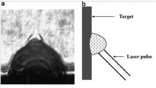
Before talking about the experimental work I would to focus the attention on the mechanism of PLAL with its advantages and disadvantages. During the laser ablation of a target both in gas phase and in liquid phase it’s generated a plasma made of the atoms constituting the target. Indeed the plasma plume is generated by laser pulse irradiating the surface of the solid target as shown in fig.19 (b). Since the temperature in the vapor plume can rise to much high values, a plasma plume will be generated during the front part of the incident laser pulse irradiating the solid target as shown Fig. 19 (a) and (b). The condensation of this plasma generates the products of PLA. Yang et al. [8] report in our work a scheme of the most important steps in the formation of the products in a PLA process in gas phase.
Figure 19. (a) The shadowgraph image of the plasma plume from the laser ablation in the gas phase. (b) The generation of the laser-induced plasma on the surface when the
front part of the laser pulse ablating the target
First, as said before, we notice the formation of plasma plume due to the interaction between laser pulse and target material. It is known that, the ablation mechanisms generating the formation of the plasma plume are different for the nanosecond and picosecond and femtosecond, laser pulses. We are interested about the ablation of the nanosecond laser, in which the material expulsion is controlled by thermal processes [9].
In the case of nanosecond laser ablation, photons can couple with both electronic and vibrational modes of the target material and moreover, this interaction produces an immediate rise in the electron temperature and eventual vaporization of the target as reported in fig. 20
Figure 20. (a) The free expansion of the laser-induced plasma in vacuum or gas when the plasma absorbed the later part of the laser pulse. (b) The ejection of the plasma
plume from the target
The evaporated material after the vaporization process, will interact with background gas, yielding the confinement of the plume, whereas the background gas is pushed further away from the solid target. Inside the plasma plume there are many neutral atoms, ions, and electrons deriving from the target solid. The electron contribution is usually present in the formation of the plasma plume only in the case of nanosecond laser
ablation, and this behavior is due to the photon-electron coupling could lead to a rapid excitation of the electron distribution. Usually the interface between the plasma plume and solid target, during the laser ablation, is in the gas state because of the high temperature of the plasma, due to irradiation by the laser pulse. The temperature of the plasma plume could rapidly reach the equilibrium and this phenomena is due to the interaction of ion and electron which accelerating their movement increase the collisions in the plasma plume [10]. Therefore, during the ablation using the nanosecond laser pulse, after the creation of the plasma plume, the later part of the incident laser pulse both directly irradiates the plasma plume and continually ablates the solid target through the plume. So in the case of nanosecond laser this plays two roles in the transformation stage of the plasma plume. The first one is, the irradiation of the target with the excitation and ionization of the species in the plume and in the second step, the later part of the laser pulse continually irradiates the interface between the plasma plume and the target and this phenomena continue to ablate more species into the plume, and then causes the plume to expand further. This second step leads to a rapid expansion of the plasma plume in vacuum, and also heats the plasma plume at higher temperature and higher species’ density as shown in Fig. 20(a) . Due to the react effect [11], the plasma plume is ejected from the surface of the target as shown Fig. 20(b). The last step of the evolution of the plasma plume created by PLA is cooling down and condensation in vacuum and the ambient gas.
Figure 21. (a) The ejection of the plasma plume from the target and (b) condensations of the laser-induced plasma
The fig. 21(a) and (b) shows the evaporation and formation of the plasma plume in gas phase. In fig. 21 (a) is reported simply the evaporation of plasma plume and in fig. 21 (b) it’s reported the condensation of the plasma freely assisted by a cool ambient gas to form nanoparticulates. The laser ablation of a target in liquid presents some difference in the formation and evolution of plasma plume. The most important difference between laser ablation of solids in vacuum or diluted gas and in liquids is that liquids confine the movement of the plasma plume. The liquid confinement, in the case of laser ablation of solids in liquid environments, change some series of processes, previously analyzed, as for instance generation, transformation, and condensation of the plasma
plume in the case of laser ablation of solids in gas phases. This confinement from liquids can induce some changing in the kinetic and thermodynamic properties of the evolution of the plasma plume and for this reason it’s possible to distinguish, from these changes, the different environments used in laser ablation. Therefore, studying the evolution of the plasma plume in laser ablation in liquids it’s possible to know the potential in technology such as materials processing.
The generation of the plasma plume from the solid target it’s caused by the interaction between the laser pulse and the surface of the solid target like in the case of the ablation in gas phase, with only one difference rather the confinement of the plasma plume by the surface tension of the liquid environment. This is schematically illustrated in Fig. 22(a).
The main difference between the two environments is in the growing and expansion of the plume. In the case of PLA in vacuum and in diluted gas, the expansion of the plasma induced by the laser is confined by the liquid. The confinement of liquids induces the plasma into a different thermodynamic state compared to the laser ablation in gas environments. This confinement is reported in the figure 20 (b).
Figure 22. The evolution of the laser-induced plasma in liquid. (a) The generation of the laser-induced plasma. (b) The expansion of the plasma plume in liquid
Fabbro et al. studied that the confinement of the plume caused by liquid environment produce a shock wave inside the plasma plume induced by the laser ablation.
The plasma plume expands its volume at a supersonic velocity and this phenomena creates a shock wave under the confinement of liquid. When the later part of the laser pulse hits the solid target another amount of the vaporizing species is generated. Then, this shock wave produces an extra pressure in the plasma and this pressure causes an increasing of the temperature of the plume.
Figure 23. (a) Some example of chemical reactions during the laser ablation of a target in liquid. (b) Condensations of the plasma plume in liquid
Therefore, this growth mechanism of plasma plume due to the confinement of liquid leads it into a thermodynamic state of the higher temperature, higher pressure and higher density, see fig. 22 (b), than that the plasma plume generated in the case of the laser ablation in gas phase. From studies conducted by Peyre et al. et al. [12] they noticed a pressure of the plasma plume in liquid of 5 GPa for a period of the laser pulse of 30 ns but they also noticed that for the shorter laser pulse of 3 ns allows to have a pressure of 10 GPa. Indeed, the wavelength, the power and the duration of the laser pulse can influence the value of the plasma-induced pressure [13]. Inside the plasma there is a temperature of 4000–5000 K, when a 532 nm Nd:YAG laser with pulse duration of 10 ns and power of 1010 W is used to ablate a isotropic graphite target in water. I would underline that the thermodynamic state with high pressure, high
temperature, and high density promote the formation of the metastable phases that are in the high-temperature and high-pressure region on their thermodynamic equilibrium phase diagram.
Yang shows in figure 23 (a) some kinds of chemical reactions would take place in the plasma plume and the interface between the liquid and the laser-induced plasma. The first kind of chemical reaction appears inside the laser-induced plasma. When inside high-density plasma there is high temperature and high pressure, the new phase, especially the metastable phase, is formed by the high temperature chemical reactions between the ablations from the target. Another kind of chemical reaction, between the reactant species are from the target and the liquid, also takes place inside the laser-induced plasma. As said before, the high pressure and high temperature in front of the laser-induced plasma lead to the excitation and evaporation of the liquid molecules at the interface between the laser-induced plasma and the liquid, and create the new plasma of the liquid molecules at the interface. After that there will be some chemical reactions between the species from the laser ablating target and the species from the liquid molecules creating some chemical species which are different from the species constituting the target and the liquid. The last step of the evolution of the plasma plume in a process of PLA of a target in liquids is cooling down and condensation in the confining liquid shown in Fig. 23(b).
As described above laser ablation of a target in liquid environment permits us to fabricate and create some chemical compounds which are different from the composition of the target. Indeed by the reactions
occurring between the plasma plume and the liquid environments it’s possible to form some kind of interesting nanostructures exploiting the metastable conditions available inside the plasma.
For these reasons we decided to synthesize MoS2 fullerene-like by the using of PLAL and following I’m going to describe my experimental work.
The experimental evidences allow us to propose a growth mechanisms for the MoS2 nanostructures formation in agreement with literature data. Solutions were prepared ablating a polycrystalline MoS2 target (the absorption coefficient at 532 nm ∼105 cm−1) was obtained pressing MoS2 commercial powder (Aldrich) for 10 min at 10 t. The ablation has been conducted using a 532 nm radiation coming from a Neodymium-Yttrium Aluminum Garnet (Nd:YAG) laser with a 5 ns pulse duration and a 10-Hz repetition rate. A sintered MoS2 target was cleaned in an ultrasonic bath using several solvents to remove organic contaminations and it was placed at the bottom of a glass vessel filled with the chosen liquid. The thickness of the liquid above the target was about 15 mm, and the ablation time was maintained at around 15 min. The laser beam was focused on the target using a 10 cm focal lens placed above the vessel as shown in the figure 24. After 15 min of irradiation a brownish solution is obtained. Used fluences ranged between 1 and 10 J/cm2 in order to test the best production rate. Ablation was performed in water (Millipore grade) and n-decane (Analytical grade from Carlo Erba).
Figure 24. Typical experimental setup to ablate a solid target in a liquid environment
After the ablation, as-produced solutions have been filtered with 0.2 µm pore size filters to remove any gross particulate matter and then drop-casted on HF cleaned silicon substrates in order to perform X-Ray Photoelectron Spectroscopy (XPS) analysis. XPS spectra have been recorded using an AXIS-ULTRA spectrometer with a basic pressure of 10−9 Torr. The X-ray radiation was generated by an Al Kα line decay (1486 eV) at operating conditions of 18 kV and 13 mA. Emitted photoelectrons were analyzed with a hemispherical electron energy analyzer. Detailed spectra have been acquired with a resolution below 1 eV. The obtained solutions were also drop-casted on copper grids for
Liquid
Solid Target
Lens
Transmission Electron Microscopy (TEM) characterization. Images were acquired using a JEM 2010F JEOL microscope operating with an acceleration voltage of 200 kV.
TEM images, reported in Fig. 25, reveal a large number of structures produced at the nanometric size range.
Figure 25. (a) TEM image of MoS2 (A) and MoO3 (B) IF-nanostructures; (b) TEM
image of MoS2structures with different shape
At least two of them were identified and labeled with letters a and b in Fig. 25 a. The first one (a) can be attributed to hollow fullerene-like MoS2 clusters [14]. The identification is due to the presence of peculiar features, such as the interlayer spacing of 0.6 nm and the polyhedral closed cage structure, thermodynamically more stable than the isolated
basal sheets of a sulphide lamellar structure [15]. The inner part of the cages seems to present a solid core. In some cases MoS2 nanostructures with different shapes have been observed as well. For instance, Fig. 25 b reports multi-walled clusters where sulphide layers (same interlayer distance of 0.6 nm) are stacked to form flat planes instead of curved surfaces. Such kind of nanoparticles could be the result of direct fragmentation processes of the target or of a successive size reduction due to laser (re)irradiation. Indeed the phenomenon of progressive laser fragmentation during PLAL has been already observed during the irradiation of metallic targets and has been recognized as an active mechanism during PLAL at appropriate wavelengths [16].
Furthermore nanoparticles size distributions are reported in the graphic 1 in which is possible to notice that the distribution for MoS2 and MoO3 , even though slightly shifted, are located in the same size range suggesting a correlation between the formation of sulphides and oxides.
N
u
m
b
e
r
o
f
p
a
rt
ic
le
s
(
a
.u
.)
MoO
3
5
10
15
20
25
Particle size (nm)
MoS
2
Graphic 1. Size distribution of the nanoparticles produced after laser ablation in water
Other particles with different crystalline arrangement have been evidenced by TEM observations and labeled with the letter B in Fig. 25 a. Lattice fringes are evident in the image and suggest that the particle is a single crystalline MoO3 cluster on the basis of the interlayer distances (0.35nm), in agreement with literature data [17]. A nanoscopic elemental analysis has been also reported in Fig. 26.
Figure 26. Comparison between the elemental sulphur map (a) and the electron image (b) in the same region. The arrow indicates a MoO3 nanoparticle
There we display a large area which includes several nanoparticles, comparing an electron image (Fig. 26b) with the respective sulphur map (Fig. 26a). The arrow indicates an oxide nanoparticle where the sulphur signal is absent. Such a result is at the same time obvious and intriguing. First of all it must be observed that, during the ablation of the MoS2 target by nanosecond laser pulses, the interaction of the front part of the laser pulse creates vapours above the target surface which are irradiated by the tail part of the same pulse. This leads to photoionizations and to the creation of a dense, high-temperature, and high-pressure laser plasma plume, which expands into the liquid. During this expansion phase, the plasma plume interacts with the surrounding liquid, creating cavitation bubbles, which, upon their collapse, give rise to extremely high temperature and pressure see Figure 27.
Figure 27. Cartoon of the cavitation bubble and n nanoparticles during the PLAL
As previously mentioned in the beginning of this chapter i condition, dissociation of MoS
presence of molybdenum ions and reactive oxygen
Cartoon of the cavitation bubble and nucleation and growth of the nanoparticles during the PLAL
As previously mentioned in the beginning of this chapter in such a condition, dissociation of MoS2 and water happens, giving rise to the presence of molybdenum ions and reactive oxygen species. Of course, such a rise to the species. Of course,
these conditions are compatible with the formation of stable oxide species and the formation of MoO3 is highly probable. As reported in literature, molybdenum oxides are essential precursors for the formation of IF-MoS2 nanostructures [18]. As said before the reaction path is generally divided into two distinguishable stages: a first surface reaction during which the surface oxide nanoparticle is converted into 1-2 closed monolayers of metal disulphide [19] and a second step consisting in a slow diffusion of sulphur atoms from the vapour plume through the growing sulphide layers to the oxide core of the nanoparticle. Considering that atomic diffusion rates vary exponentially with temperature, it is clear that high temperatures (several thousand of degrees) reached during the PLAL process dramatically shorten the time required to complete the reaction. The conversion of molybdenum oxide into IF-MoS2 implies the condensation of molecular Mo3O9 clusters into substoichiometric MoO3−x nanosize particles, which undergo subsequent sulphidization. From what said before, it is really hard to affirm if the formation of IF-MoS2 is due to direct condensation of atomic/molecular species in the plasma or to a multistep process which involves the synthesis of oxides or suboxides species. Moreover, it seems that no literature data report specific information about the bonding states and the chemical nature of material produced in the case of IF-MoS2 synthesis with far-fromequilibrium processes (laser ablation, arc discharge and electron beam irradiation), so XPS analysis were carried out in order to obtain further information about the chemical nature of
obtained species and to try to elucidate the possible reaction routes involved in the formation of IF-MoS2.
Mo3d signal (left side, Fig. 28) indicates the presence of a predominant amount of MoVI signals, assigned to MoO3.
Figure 28. Mo3d and S2p XPS spectra obtained on the ablated materials in pure water, after filtration and deposition onto a substrate (black line). The S2p signals have been decomposed according to literature data. The figure also reports the spectra relative to
MoS2 (red line) and MoO3 (blue line) bulk target
Signals belonging to MoS2 are located at lower binding energies as shown in the same figure. In this range of energy XPS spectra show a
150 160 170 220 230 240 M oS2 S 2p sulphate 3/2 MoO 3 sulphate 1/2 S-S 1/2 S-S 3/2 M oS 2 1/2 M oS 2 3/2 M o3d M oS2 Deposit In te n s it y ( a .u .)
continuum of electronic states which could belong either to MoS2, to oxysulphates or to metal oxides at a lower oxidation state. The observation of the S2p region seems to offer to an easier interpretation. It is possible to point out three different sulphur-containing chemical species, each one giving 3/2 and 1/2 spin–orbit doublets. These doublets fall at 162.3-163.6 eV, 163.7-164.9 eV and 169.2-170.5 eV and can be easily assigned to MoS2, external sulphur and sulphates respectively, on the basis of literature data [20]. With the attribution of “external sulphur” we indicate both polysulphides and elemental sulphur, since these two compounds are not distinguishable in the XPS spectrum on the basis of B.E. values. Elemental sulphur could be present in our system in the form of linear chains with sulphate groups at the end of each chain. As reported by Steudel [21], such structures have been already found in aqueous solution. The presence of the sulphur is due to the incongruent melting of MoS2 which decomposes above 1185 °C. The formation of stable molybdenum oxide species including MoO3, sub-oxides and oxysulphates raises a problem about the nature of oxidation of molybdenum, which is if oxide has to be considered as by-product or if it plays a crucial role in the formation of MoS2 fullerene-like nanostructures. As previously mentioned, MoO3 and molybdenum suboxides (MoO3-x) can react at high temperature with sulphur to produce MoS2:
+ 2 → +2 + 7 − 2 → + 3 − 2
From what described, we suppose that IF-MoS2 nanoparticles found by TEM have been formed in a multistep process at high temperatures during the ablation process.
When the ablation ends, the multistep reaction stops and all the species involved in the reaction path (MoO3, MoO3-x and MoS2) can be found in the obtained solution. Based on these considerations, the proposed reaction path would not be possible in an oxygen-free solvent, since the formation of the MoO3 species in the plasma would be inhibited. To confirm this, laser ablation of MoS2 was performed also in n-decane, at the same conditions as in the previous experiment. In this case, TEM analysis does not show any relevant structure. Moreover XPS spectra of the filtered system do not reveal the presence of Mo signals. These results can be explained in two ways. It could be possible that carbonaceous contaminations (coming from the partial pyrolysis of the hydrocarbon during the ablation process) form a shell surrounding each produced particle, that avoid the detection of the underlying molybdenum. This effect has been already observed during the ablation of silver and iron targets and reported so far [22]. If the carbon shell is thicker than 5 nm, no electrons from the Mo atoms can be detected, due to the low mean-free path of electrons in the material.
On the other hand, if the formation of MoO3 is a fundamental intermediate step for the growth of IF-MoS2, no Mo-containing nanostructures are formed in the plasma during ablation and only “macrofragments” of MoS2 sheets bigger than 200 nm, are removed from the target.
These fragments are retained in the filtration step before the XPS analysis. If the ablation is performed in water, the presence of reactive oxygen species during the particle formation could come from the breakdown of water molecules and the presence of molecular oxygen dissolved in the liquid. For this reason we performed an ablation experiment purging the liquid with molecular nitrogen, which is one of the most common and effective techniques for the removal of dissolved oxygen from water. This certainly reduces the amount of reactive oxygen available. In such a case, while TEM observations do not reveal any significant variations with respect to the un-purged case, XPS data show some significant differences. In Fig. 29a Mo3d and S2p XPS regions of the sample obtained by ablating the MoS2 target in water under nitrogen flux are shown.
Figure 29. Mo3d and S2p XPS spectra obtained on the ablated materials in pure water purged with a N2flux (black line). The filtrated sample has been deposited onto a
substrate. The S2p signals have been decomposed according to literature data. The figure also reports the spectra relative to MoS2 (red line) and MoO3 (blue line) bulk
target
The S2p region shows that the amount of MoS2 and sulphates are significantly lower with respect to external sulphur if compared with those observed in absence of nitrogen purging (see Table 1).
160 170 2 20 230 240
In
te
n
s
it
y
(
a
.u
.)
S 2p M o3d M oS 2 M oO 3 M oS2 D epositB inding E nergy (eV )
M oS 2 1/2 M oS 2 3/2 S-S 3/2 S-S 1/2 sulphate 3/2 sulphate 1/2
sulphate S-S bonds MoS2
11 at. % 76 at. % 13 at. % Not purged 49 at. % 32 at. % 19 at. % Purged
Table 1. Quantitative XPS results obtained comparing N2 purged and unpurged
This clearly indicates that, in a poor oxidant medium, only a small fraction of the material ablated leads to the formation of MoS2 nanostructures, while the most part of it gives the formation of S-S bonds (polysulphides or elemental sulphur). Moreover, we can observe that the Mo3d spectrum reported in Fig. 29 is completely different from the one in Fig. 28. In details, the spectrum in Fig. 29 presents nearly a continuum of states at higher B.E. values, indicating that, together with completely oxidized Mo, different lower oxidation states can be found and suggesting the presence of a larger quantity of substoichiometric oxides. These species are observed with an oxidation state between Mo4+ (MoS2) and Mo6+ (MoO3) and, for this reason, the Mo signal is shifted with respect to the reference signal in Fig. 28. A proper deconvolution of the obtained spectra based on literature assignation [21] can be found in the (Fig. 30).
225 230
235 240
245
Binding Energy (eV)
Overall fit S2s (MoS2 ) S2s (external S) Mo3d (MoOx) Mo3d (MoO3) Mo3d (MoS2)
Figure 30. XPS spectrum in the Mo3d region relative to the ablated material obtained by a PLAL procedure in pure water, purged with a N2 flux
The figure shows a deconvolution into several components as suggested by literature data. This deconvolution takes into account the presence of either stoichiometry molybdenum oxide and sub-stoichiometry species (spin-orbit doublets with the same colour in the figure). In the same spectral region S2p signals (single component) have to be considered taking into account the presence of external sulphur, sulphates and