Nanocarbons syntheses for
advanced electrical and thermal
applications
Rosangela Piscitelli
Unione Europea UNIVERSITÀ DEGLI STUDI DI SALERNO
FONDO SOCIALE EUROPEO
Programma Operativo Nazionale 2000/2006
“Ricerca Scientifica, Sviluppo Tecnologico, Alta Formazione” Regioni dell’Obiettivo 1 – Misura III.4
“Formazione superiore ed universitaria”
Department of Industrial Engineering
Ph.D. Course in Chemical Engineering
(XV Cycle-New Series, XXIX Cycle)
NANOCARBONS SYNTHESES FOR
ADVANCED ELECTRICAL AND THERMAL
APPLICATIONS
Supervisor
Ph.D. student
Prof. Maria Sarno
Rosangela Piscitelli
Scientific Referees
Prof. Paolo Ciambelli
Prof. Claudio Ampelli
Dott. Sergio Galvagno
Ph.D. Course Coordinator
Ringraziamenti
Desidero ringraziare tutti coloro che hanno contribuito alla
realizzazione di questo lavoro.
Un ringraziamento speciale alla Prof.ssa Maria Sarno che ha creduto
in me fin dal primo momento e mi ha sostenuta con grande energia
determinazione e professionalità dal primo all’ultimo giorno di questo
difficile ed agognato percorso.
Ringrazio sentitamente il Prof. Paolo Ciambelli per avermi fatto da
guida, per la sua visione di insieme e per la professionalità che da
sempre lo contraddistingue.
Grazie alla Dott.ssa Claudia Cirillo per il suo fondamentale contributo
nella realizzazione di questa tesi. Grazie per la disponibilità, la lealtà e
l’amicizia che mostra sempre nei miei confronti.
Ringrazio inoltre il gruppo del dipartimento “Ambiente Cambiamenti
Globali e Sviluppo Sostenibile” dell’ENEA che si occupa della
preparazione del carburo di silicio per avermi consentito di poter
lavorare su questo materiale così interessante.
Ringrazio Claudio per essere stato al mio fianco in ogni momento di
questo percorso, per la pazienza, l’aiuto e la disponibilità che non mi
fa mai mancare.
Ringrazio mia madre per aver avermi spronata in ogni momento di
difficoltà.
Pubblicazioni
“Supercapacitor electrodes made of exhausted activated carbon derived SiC nanofilamment coated by graphene” Sarno M., Galvagno S., Piscitelli R., Portofino S., Ciambelli P. Industrial Engineering Chemistry Reserch 55 (20) 2016
“New Designed procedure for G/SiO2/SiC Nano-heterojunctions growth on recycled 3C-SiC powder” Sarno M., Galvagno S., Piscitelli R., Portofino S., Cirillo C., Ciambelli P. Chemical Engineering Transaction Vol. 57 2017 Accepted
“Experimental, Moodelling and theoretical study of CNT growth and connection on a flip- chip Device to improve thermal management performances” Sarno M., Piscitelli R., Marra F., Cirillo C., Ciambelli P. Chemical Engineering Transaction Vol. 57 2017 Accepted
“Raman Spectroscopy to measure carbon nanotubes thermal conductivity” M. Sarno, R Piscitelli, C. Cirillo, 2017 Carbon Submitted
“Microsupercapacitor based on graphene”. “International Conference on Advanced Energy Materials” M. Sarno, R. Piscitelli. September 2017, England Submitted.
Index
Chapter I ... 13 Nanocarbons synthesis ... 13 Atomic Structure ... 18 Properties of graphene ... 18 Density of graphene ... 18 Electronics properties ... 19 Mechanical Properties ... 19 Optical Properties ... 20 Thermal Properties ... 20 Chemical properties ... 21 Applications of graphene ... 21 Graphene production ... 22 Micromechanical Cleavage ... 23Epitaxial Graphene from Silicon Carbide ... 23
Chemical Exfoliation ... 24
Graphene grown on transition metal surfaces using Chemical Vapour Deposition (CVD) ... 25
Transfer of graphene grown on metals ... 26
Multi-Walled Carbon Nanotubes ... 28
Arc discharge and Laser ablation ... 28
Arc discharge ... 29
Plasma arc Jet ... 30
Laser ablation ... 30
Single-Walled Carbon Nanotubes ... 37
Chapter II ... 43
Graphene and graphene/SiO2 composites on exhausted activated carbon derived 3C-SiC powders. ... 43
Graphene growth on SiC. ... 43
C/SiO2/SiC core layers sheath nanofilaments ... 45
Experimental ... 46
Material and methods ... 46
Preparation of SiC from exhausted activated carbon ... 46
Preparation of Graphene/SiC and few layer carbon/SiO2/SiC ... 47
Characterization Methods ... 48
Results and discussion ... 48
SiC characterization ... 48
G/SiC and FLG/SiO2/SiC characterization ... 56
C/SiO2/SiC characterization ... 62
Supercapacitors application ... 75
G/SiC supercapacitor performance evaluation ... 77
Conclusion ... 88
Chapter III ... 91
Conductive carbon nanotubes for Thermal Management ... 91
Carbon nanotubes synthesis: experimental, results and discussion. ... 92
Numerical analysis ... 94
Conclusions ... 102
List of Figures
Figure I.1 Images of crystal structure of: graphite (a) and diamond (b) ... 14 Figure I.2 Carbon allotropes from 0D to 3D ... 15 Figure I.3 Structure of graphene: an atomic-scale honeycomb lattice made of carbon atoms ... 17 Figure I.4 The honeycomb atomic lattice structure ... 17 Figure I.5 Scheme of the micromechanical cleavage technique (‘Scotch tape’ method) for producing graphene “Novoselov (2011)”(a), Images of:
graphite flake cleaved by Scotch tape (b) tape covered with graphite pressed down on silicon wafer (c) ... 24 Figure I.6 Liquid-phase exfoliation of graphite method ... 25 Figure I.7 Scheme of the growth process for the synthesis of graphene using CVD ... 26 Figure I.8 Scheme of the graphene transfer process to a substrate “Bae et al.(2010)” ... 27 Figure I.9 Scheme of roll-to-roll process for the transfer of FLG from Ni foil to EVA/PET substrates “Juang et al. (2010)” ... 28 Figure I.10 Arc-discharge schematic experimental setup ... 29 Figure I.11 TEM image of carbon nanotubes produced by arc discharge ... 30 Figure I.12 Laser ablation schematic experimental setup ... 31 Figure I.13 TEM images of carbon nanotubes produced by laser ablation method (a); tube wall particular (b). ... 31 Figure I.14 CVD schematic experimental setup ... 32 Figure I.15 TEM images of carbon nanotubes produced by CVD method .. 33 Figure I.16 Schematic diagram of the growth process ... 35 Figure I.17 SEM images of aligned carbon nanotubes obtained by the pyrolysis of ferrocene, images a) and b) show views of the aligned nanotubes along and perpendicular to the axis of the nanotubes respectively ... 36 Figure I.18 HRTEM image of SWNTs obtained by arcing graphite electrodes ... 38 Figure I.19 HRTEM image of the ends of SWNTS ... 39 Figure I.20 HRTEM image of SWNTs obtained by the pyrolysis of
nickelocene and C2H2. (flow rate= 50cm3/min) at 1100°C in a flow Ar (1000
cm3/min) ... 40 Figure I.21 HRTEM image of SWNTs obtained by the prolysis of Fe(CO)5
and C2H2 (flow rate= 50cm3/min) at 1100°C in a flow Ar (1000 cm3/min) 41
Figure II.1 X-ray diffraction pattern of the synthesized 3C-SiC ... 49 Figure II.2 SEM images of the produced SiC at increasing magnification .. 50 Figure II.3 TEM image of the SiC nanofilaments. The inserts show: an higher-magnification image, an FFT and electron diffraction patter ... 51 Figure II.4 EDX spectrum collected on the all image ... 52 Figure II.5 Raman spectrum of the synthesized 3C-SiC ... 53
Figure II.6 Thermogravimetric test on the synthesized SiC: TG in green,
DTG in blue ... 54
Figure II.7 XRD spectrum obtained on the powder after the thermo gravimetrical test ... 54
Figure II.8 Nitrogen adsorption-desorption isotherm for SiC nanofilament 55 Figure II.9 Pore-diameter distribution curves of the synthesized SiC ... 56
Figure II.10 Raman spectrum of graphene SiC, 2D peaks deconvolution.... 57
Figure II.11 TEM image of three layers graphene on SiC ... 58
Figure II.12 Concentration profiles of H2 and CH4 during the graphene synthesis test ... 59
Figure II.13 TEM image of C/SiO2/SiC ... 62
Figure II.14 Representative TEM images of the prepared nanofilaments of C/SiO2/SiC composite. High resolution TEM images of coaxial nanowhiskers, displaying single crystalline 3C-SiC core, SiO2 intermediate layer and outer graphitic carbon sheaths. Energy dispersion spectra taken from different zones of the nanofilament as marked in the insert of (a) with A, B and C ... 63
Figure II.15 Raman spectrum of C/SiO2/SiC ... 64
Figure II.16 X-ray diffraction spectrum of C/SiO2/SiC ... 65
Figure II.17 Oxide thickness vs reaction time ... 75
Figure II.18 TG-DTG-MS of G/SiC: TG in green; DTG in blue; DSC in maroon; MS in orange ... 80
Figure II.19 Nitrogen adsorption-desorption isotherm (a) and pore-diameter distribution (b) curves of G/SiC ... 82
Figure II.20 Cyclic voltammetry, in the range 0-1V, of SiC (a), G/SiC (b). . 83
Figure II.21 Galvanostatic charge/discharge curves of SiC (c) ... 84
Figure II.22 Galvanostatic charge/discharge curves of G/SiC ... 84
Figure II.23 Specific capacitance of SiC and G/SiC electrodes at different scan rate ... 85
Figure II.24 Capacitance retention at 4 A/g ... 85
Figure II.25 Ragone Plot for G/SiC and SiC (a). Cyclic voltammetry of G/SiC in the range -0.5-0.5 V ... 87
Figure III.1 SEM image of AlN covered by a CNT forest (a, b). Photo of AlN covered by CNT forests, Au covers some areas of the devices ... 93
Figure III.2 Raman spectra at two different laser power ... 94
Figure III.3 Sketch of flip-chip and planar view of the device. ... 96
Figure III.4 Temperature profile along x axis gained at different bumps heights and with K=60 W/mk. Temperature profile Vs thermal conductivity at the device centre for different bumps’ connection height. ... 98
Figure III.5 Temperature profile along x axis at bumps heights of 10 µm, with K=60W/mk and Au layer ... 99
Figure III.6 Left side: device Temperature with bumps’ connection height of 10 µm and with Au layer Kbumps=300 W/mk. Right side: Temperature profile along x coordinate (bumps height of 10µm). ... 100
Figure III.7 Temperature result differences between 6 and 13 bumps
Abstract
Carbon nanotubes are unique nanostructure with remarkable electronic, mechanical and thermal properties, some stemming from the close relation between carbon nanotubes and graphite, and some from their one-dimensional structure. Since their exceptional and suitable properties (high thermal and electrical conductivity, high thermal stability, relevant mechanical and field emission properties) they have soon attracted great attention.
Graphene is the first two-dimensional (2D) atomic crystal available to us. Since its discovery in 2004, graphene has captured the attention and the imagination of worldwide researchers thank to its supreme properties.
Carbon nanotubes and graphene are considered today the building blocks of nanotechnology.
In such light, this thesis work has been focused to develop industrial scalable processes, starting from research at lab scale on carbon nanotubes and graphene formation, to explore their potentialities for electrical and thermal applications, e.g. microelectronic devices.
In particular, graphene has been obtained at atmospheric pressure and low temperature on exhausted activated carbon-derived SiC nanoparticles (Chapter II). The graphene’s growth, traced by online analyzers, has been obtained from an external source of carbon, in particular by methane/hydrogen chemical vapor deposition (CVD). Recycled SiC has been chosen as growth substrate to carry out a convenient process and to increase the added value of the recycled, combining the favorable properties of different substances. Therefore, the SiC powder and the composite material obtained have been carefully characterized by the combined use of different techniques and tested for energy storage applications, e.g. due to their “fine pitch” for microsupercapacitor. The results show a very high capacitances up to 114.7 F/g for SiC alone and three times higher in the presence of graphene with an excellent cycle stability
Moreover, few layer graphene/SiO2/SiC (G/SiO2/SiC) core-layers-sheath nano-heterojunctions were obtained (Chapter II) by a new easy and cheap designed procedure by thermal annealing at atmospheric pressure and low temperature on the SiC powder. The advanced materials obtained were carefully characterized by the combining use of different techniques: transmission electron microscopy (TEM) with EDAX probe, scanning electron microscopy (SEM), X-ray diffraction analysis, Raman spectroscopy, thermogravimetric analysis coupled with quadrupole mass detector (TG-DTG-MASS).
Finally, in Chapter III an experimental, modelling and theoretical study of CNT growth and connection on a chip device with a flip chip
configuration used to improve thermal management performances, in order to elaborate board design analysis, was reported. CNTs growth was obtained for the first time on AlN substrate typically used in high power electronic. An innovative technique was developed to measure thermal conductivity, of 1698,5 W/mK, for an isolated CNT. Moreover, the aim of the work was to study the role of the design parameters to mitigate the effects of a non-correct thermal management obtained with the help of high thermal conductive CNT connections bumps.
With the support of a COMSOL MULTIPHYSICS simulator we evaluated thermal performances to help in a preliminary phase the board design. We worked on a configuration that would allow the direct integration into flip-chip devices in order to reduce the thermal contact resistance at interfaces from the die through the heat spreader and the junction temperature and thermal crosstalk.
Introduction
Carbon nanomaterials such as carbon nanotubes (CNT) or graphene, are interesting materials for future microelectronics due to their outstanding electrical, mechanical and optical properties as well as their high surface area.
Carbon nanotubes (CNTs) are an allotrope of carbon, consisting in a graphene rolled into a tube.
Carbon Nanotubes can be achieved by several techniques, e.g. Arc discharge and Laser ablation, Plasma arc Jet, Chemical Vapor deposition (CVD).
Graphene is a flat monolayer of carbon atoms tightly packed into a two-dimensional (2D) honeycomb lattice, and is a basic building block for graphitic materials of all other dimensionalities.
Graphene can be achieved through different methods, like mechanical exfoliation using “scotch tape method”, liquid-phase exfoliation of graphite exposing the materials to a solvent, epitaxial growth on SiC.
Starting from research at lab scale on carbon nanotubes and graphene a large scale and economical synthesis of three different nano-materials for several microelectronic applications was carried out.
In particular, the studies were focused on:
- The realization of graphene on recycled SiC to achieve a nano composite material tested for energy storage applications, e.g. due to their “fine pitch” for microsupercapacitor.
- The development of a nano-heterojunctions made of few layer graphene/SiO2/SiC core-layers-sheath obtained by a new easy and cheap designed procedure by thermal annealing at atmospheric pressure and low temperature on the 3C-SiC powder derived from exhausted activated carbon.
- An experimental, modelling and theoretical study of CNT growth and connection on a chip device with a flip chip configuration used to improve thermal management performances, in order to elaborate board design analysis. Thermal performances of this device have been evaluated with the support of COMSOL MULTIPHYSICS simulator. An innovative technique to measure thermal conductivity for an isolated CNT was developed.
Objectives
The goal of the research has been to develop industrial scalable processes starting from research at lab scale on carbon nanotubes and graphene formation, to explore their potentialities for electrical and thermal applications, e.g. microelectronic devices.
In particular, the targets have been:
The preparation of graphene at atmospheric pressure and low temperature on exhausted activated carbon-derived SiC nanoparticle, for supercapacitor applications.
The preparation of few layer graphene/SiO2/SiC core-layers-sheath nano-heterojunctions.
The CNT growth and connection on a high power amplifier device with a flip chip configuration to improve thermal management performances using an experimental, modeling and theoretical study with COMSOL MULTIPHYSICS simulator.
To develop an innovative technique to measure thermal conductivity for an isolated CNT.
Chapter I
Nanocarbons synthesis
Carbon is the element in the periodic table that provides the basis for life on Earth. It is also important for many technological applications, ranging from drugs to synthetic materials. This role is a consequence of carbon’s ability to bind to itself and to nearly all elements in almost limitless variety. The resulting structural diversity of organic compounds and molecules is accompanied by a broad range of chemical and physical properties.
Carbon, one of the most common element on Earth, occurs naturally in many forms and as a component in countless substances.
Carbon has long been known to exist in three forms, namely, amorphous carbon, graphite, and diamond (Figure I.1) “Dai et al. (2012)”.
Depending on how the carbon atoms are arranged, their properties vary. For example, graphite is soft and black and the stable, common form of carbon with strong covalent bonding in the carbon plane and the much weaker van der Waals interactions in the transverse direction between the layers (Figure I.1 a). Graphite's common usage is as the core of a pencil, where flakes of graphite slide off the bulk material and remain as a mark on paper.
Diamond is hard and transparent with each carbon atom bound to four other carbon atoms in a regular lattice (Figure I.1 b). It is constituted by a crystal lattice of carbon atoms arranged in a tetrahedral structure. Each carbon atom thus forms four covalent bonds with four neighboring atoms, completely filling its outer electron shell and resulting in one of the hardest and most valued substances in human history.
Figure I.1 Images of crystal structure of: graphite (a) and diamond (b)
But, in the last decade, three nanoscale forms of carbon have attracted widespread attention because of their novel properties: buckyballs, carbon nanotubes, and graphene.
A buckyball is created by collapsing yet another dimension. A buckyball is a small segment of a carbon nanotube that has been pinched together at both ends to form a hollow sphere of carbon atoms. The 60-carbon buckyball was the first carbon nanomaterial to gain widespread attention.
Carbon-60 (C60) is probably the most studied individual type of nanomaterial. The spherical shape of C60 is constructed from twelve pentagons and twenty hexagons and resembles a soccer ball. Buckyballs have many proposed uses, such as for example encapsulation of reactive compounds in chemistry.
Carbon nanotubes (CNTs) are another allotrope of carbon. They can be thought of as ribbons of graphene that have been rolled into a tube. Due to the strength of the bonds in a hexagonal carbon lattice, nanotubes are one of the strongest fibers ever discovered.
Actually the most recent carbon nanomaterial to be widely studied is graphene. Its basic structure is very simple: it is formed by a 6-carbon ring of atoms, and then tessellate that hexagon to form a two dimensional (2D) hexagonal honeycomb lattice. Such a 2D sheet is known as graphene.
Graphene's properties are striking in a number of respects, but probably most notable is that a single graphene sheet is quite stable and mechanically resilient, as well as very electrically conductive.
Graphene is the building block for carbon nanotubes and buckyball “Geim
and Novoselov (2007)”.
Fullerene, or buckyball, is formed by wrapping up graphene into zero dimensional (0D) buckyball; carbon nanotube is formed by rolling up graphene into 1D cylinder and graphite is formed by stacking graphene into 3D structure (Figure I.2). For example, the crystalline form of graphite consists of many graphene sheets stacked together.
Figure I.2 Carbon allotropes from 0D to 3D
Graphene-like structures were already known of since the 1960’s “Boehm et al. (1962), Van Bommel et al. (1975), Forbeaux et al. (1998), Oshima et al. (2000)” but there were experimental difficulties in isolating single layers in such a way that electrical measurements could be performed on them, and there were doubts that this was practically possible.
It is interesting to consider that everyone who has used an ordinary pencil has probably produced graphene-like structures without knowing it. A pencil contains graphite, and when it is moved on a piece of paper, the graphite is cleaved into thin layers that end up on the paper and make up the text or drawing that we are trying to produce. A small fraction of these thin layers will contain only a few layers or even a single layer of graphite, i.e. graphene.
Thus, the difficulty was not to fabricate the graphene structures, but to isolate sufficiently large individual sheets in order to identify and characterize the graphene and to verify its unique two-dimensional (2D)
properties. This is what Geim, Novoselov, and their collaborators succeeded in doing .
Ever since the discovery of the carbon nanotubes, several ways of preparing them have been explored. In particular, besides multi wall (MWNTs) and single wall (SWNTs) nanotubes have been prepared.
This chapter summarizes the progress made in recent years in growing carbon nanotubes by various methods such as arc-discharge, laser ablation and chemical vapour deposition (CVD). The growth of nanotubes materials by CVD will be focused on, because CVD is a highly promising technique in order to achieve defect-free materials by controlling the growing process during the synthesis operation.
Graphene is the name given to a flat monolayer of carbon atoms tightly packed into a two-dimensional (2D) honeycomb lattice, and is a basic building block for graphitic materials of all other dimensionalities (Figure II.1) “Geim and Novoselov (2007)”.
The term graphene was coined in 1962 as a combination of graphite and the suffix -ene by Hanns-Peter Boehm and described single-layer carbon foils. The crystalline or "flake" form of graphite consists of many graphene sheets stacked together.
In 2004 physicists at the University of Manchester and the Institute for Microelectronics Technology, Chernogolovka, Russia, first isolated individual graphene planes by using adhesive tape. They also measured electronic properties of the obtained flakes and showed their unique properties.
The Royal Swedish Academy of Sciences has awarded the Nobel Prize in Physics for 2010 to Andre Geim and Konstantin Novoselov, both of the University of Manchester, "for groundbreaking experiments regarding the two-dimensional material graphene".
A thin flake of ordinary carbon, just one atom thick, lies behind Nobel Prize in Physics. Geim and Novoselov have shown that carbon in such a flat form has exceptional properties that originate from the remarkable world of quantum physics.
Geim and Novoselov extracted the graphene from a piece of graphite such as is found in ordinary pencils. Using regular adhesive tape they managed to obtain a flake of carbon with a thickness of just one atom. This at a time when many believed it was impossible for such thin crystalline materials to be stable.
Figure I.3 Structure of graphene: an atomic-scale honeycomb lattice made of carbon atoms
However, with graphene, it's possible to study a new class of two-dimensional materials with unique properties. Also a vast variety of practical applications now appear possible including the creation of new materials and the manufacture of innovative electronics.
Since it is practically transparent and a good conductor, graphene is suitable for producing transparent touch screens, light panels, and maybe even solar cells.
When mixed into plastics, graphene can turn them into conductors of electricity while making them more heat resistant and mechanically robust. This resilience can be utilized in new super strong materials, which are also thin, elastic and lightweight. In the future, satellites, airplanes, and cars could be manufactured out of the new composite materials.
Atomic Structure
In graphene, carbon atoms are arranged in a honeycomb lattice with angles of 120° as shown in Figure II.2. The carbon-carbon bond length in graphene is about 0.142 nanometers. We can see this atomic arrangement as a combination of benzene rings with a center-to-center distance of 0.246 nanometers.
Graphene sheets stack to form graphite with an interplanar spacing of 0.335 nm, which means that a stack of three million sheets would be only one millimeter thick.
Properties of graphene
Properties of graphene are determined mainly by its structural conformation, in particular by two unique features that affect its properties and material make it truly extraordinary. The first is the structural perfection: it is formed only by carbon atoms joined together by strong bonds and at the same time flexible, forming a crystalline structure practically, completely free of defects such as atoms out of place or missing. The second peculiarity is that the electrons behave as massless particles, such as photons, with an extremely high electron mobility (), equal to 15000 cm2 · V-1 · s-1 at room temperature. This makes this unique nanomaterial and suitable for many innovative applications “Geim and Novoselov et al. (2007)”.
Density of graphene
The unit hexagonal cell of graphene contains two carbon atoms and has an area of 0.052 nm2. Thus, its density is 0.77 mg/m2 “Nobel Physics Laureates (2010)”.
Electronics properties
One of the most useful properties of graphene is that it is a zero-overlap semimetal (with both holes and electrons as charge carriers) with very high electrical conductivity. Carbon atoms have a total of 6 electrons; 2 in the inner shell and 4 in the outer shell. The 4 outer shell electrons in an individual carbon atom are available for chemical bonding, but in graphene, each atom is connected to 3 other carbon atoms on the two dimensional plane, leaving 1 electron freely available in the third dimension for electronic conduction. These highly-mobile electrons are called pi (π) electrons and are located above and below the graphene sheet. These pi orbitals overlap and help to enhance the carbon to carbon bonds in graphene. Fundamentally, the electronic properties of graphene are dictated by the bonding and anti-bonding (the valance and conduction bands) of these pi orbitals.
Combined research over the last 50 years has proved that at the Dirac point in graphene, electrons and holes have zero effective mass. This occurs because the energy – movement relation (the spectrum for excitations) is linear for low energies near the 6 individual corners of the Brillouin zone. These electrons and holes are known as Dirac fermions, or Graphinos, and the 6 corners of the Brillouin zone are known as the Dirac points. Due to the zero density of states at the Dirac points, electronic conductivity is actually quite low. However, the Fermi level can be changed by doping (with electrons or holes) to create a material that is potentially better at conducting electricity than, for example, copper at room temperature “Geim and Novoselov (2007)”.
Mechanical Properties
Another of graphene’s stand-out properties is its inherent strength. Due to the strength of its 0.142 Nm-long carbon bonds, graphene is the strongest material ever discovered, with an ultimate tensile strength of 130,000,000,000 Pascals (or 130 gigapascals), compared to 400,000,000 for A36 structural steel, or 375,700,000 for Aramid (Kevlar). Not only is graphene extraordinarily strong, it is also very light at 0.77 milligrams per square metre (for comparison purposes, 1 square metre of paper is roughly 1000 times heavier). It is often said that a single sheet of graphene (being only 1 atom thick), sufficient in size enough to cover a whole football field, would weigh under 1 single gram.
What makes this particularly special is that graphene also contains elastic properties, being able to retain its initial size after strain. In 2007, atomic force microscopic (AFM) tests were carried out on graphene sheets that were
suspended over silicone dioxide cavities. These tests showed that graphene sheets (with thicknesses of between 2 and 8 Nm) had spring constants in the region of 1-5 N/m and a Young’s modulus (different to that of three-dimensional graphite) of 0.5 TPa. Again, these superlative figures are based on theoretical prospects using graphene that is unflawed containing no imperfections whatsoever and currently very expensive and difficult to artificially reproduce, though production techniques are steadily improving, ultimately reducing costs and complexity “Geim and Novoselov (2007)”.
Optical Properties
Graphene’s ability to absorb a rather large 2.3% (97.7% transmittance) of white light is also a unique and interesting property, especially considering that it is only 1 atom thick. This is due to its aforementioned electronic properties; the electrons acting like massless charge carriers with very high mobility. A few years ago, it was proved that the amount of white light absorbed is based on the Fine Structure Constant, rather than being dictated by material specifics. Adding another layer of graphene increases the amount of white light absorbed by approximately the same value (2.3%). Due to these impressive characteristics, it has been observed that once optical intensity reaches a certain threshold (known as the saturation fluence) saturable absorption takes place (very high intensity light causes a reduction in absorption). This is an important characteristic with regards to the mode-locking of fibre lasers. Due to graphene’s properties of wavelength-insensitive ultrafast saturable absorption, full-band mode locking has been achieved using an erbium-doped dissipative soliton fibre laser capable of obtaining wavelength tuning as large as 30 nm.
In terms of how far along we are to understanding the true properties of graphene, this is just the tip of the iceberg. Before graphene is heavily integrated into the areas in which we believe it will excel at, we need to spend a lot more time understanding just what makes it such an amazing material. Unfortunately, while we have a lot of imagination in coming up with new ideas for potential applications and uses for graphene, it takes time to fully appreciate how and what graphene really is in order to develop these ideas into reality. This is not necessarily a bad thing, however, as it gives us opportunities to stumble over other previously under-researched or overlooked super-materials, such as the family of 2D crystalline structures that graphene has born “Bonaccorso et al. (2010)”.
Thermal Properties
Graphene is a perfect thermal conductor. Its thermal conductivity was measured recently at room temperature and it is much higher than the value
observed in all the other carbon structures as carbon nanotubes, graphite and diamond (> 5000 W/mK).
The ballistic thermal conductance of graphene is isotropic, i.e. same in all directions. Similarly to all the other physical properties of this material, its 2 dimensional structure make it particularly special. Graphite, the 3D version of graphene, shows a thermal conductivity about 5 times smaller (1000 W m-1 K-1). The phenomenon is governed by the presence of elastic waves propagating in the graphene lattice, called phonons.
The study of thermal conductivity in graphene may have important implications in graphene-based electronic devices. As devices continue to shrink and circuit density increases, high thermal conductivity, which is essential for dissipating heat efficiently to keep electronics cool, plays an increasingly larger role in device reliability “Zhu et al. (2010b)”
Chemical properties
Similar to the surface of graphite, graphene can adsorb and desorb various atoms and molecules (for example, NO2, NH3, K, and OH).
Weakly attached adsorbates often act as donors or acceptors and lead to changes in the carrier concentration, so graphene remains highly conductive. This can be exploited for applications as sensors for chemicals.
Other than weakly attached adsorbates, graphene can be functionalized by several chemical groups (for instances OH-, F-) forming graphene oxide and fluorinated graphene. It has also been revealed that single-layer graphene is much more reactive than 2, 3 or higher numbers or layers.
Also, the edge of graphene has been shown to be more reactive than the surface. Unless exposed to reasonably harsh reaction conditions, graphene is a fairly inert material, and does not react readily despite every atom being exposed and vulnerable to its surrounding “Bonaccorso et al. (2010)”
Applications of graphene
The extraordinary properties of graphene, carbon sheets that are only one atom thick, have caused researchers to consider using this material in many technology areas. Some of these are:
(i) Graphene-based electronics and optoelectronics, partially replacing conventional siliconbased electronics, because graphene has ultrafast terahertz electron mobility that gives it a very bright future for building smaller, faster, cheaper electronic devices such as ballistic transistors “Liang et al. (2007)”, spintronics “Yazyev et al. (2008)”, field effect transistors “Meric et al. (2008)”, and optoelectronics “Bonaccorso et al. (2010)”.
(ii) Graphene filled polymer composites with high electrical and thermal conductivity, good mechanical strength, and low percolation threshold, which, in combination with low-cost and largescale production, allow a variety of performance-enhanced multifunctional use in electrically conductive composites, thermal interface materials, etc. “Dikin et al. (2007), Stankovich et al. (2006)”.
Large-area CVD-grown graphene that is suitable to replace indium tin oxide (ITO) as cheaper, transparent conducting electrodes in various display applications such as touch screens, which is considered to be one of the immediate applications in a few years “Kim et al. (2009), Bae et al. (2010)”. (iii) Another advantage over ITO is that ITO suffers from being brittle and is incapable of bending, which does not allow it to meet the requirements for flexible devices, while graphene is a more competitive solution for flexible, transparent and processable electrodes.
(iv) Graphene-based electrochemical storage energy devices such as high-performance Lithium Ion Batteries (LIBs) and ElettroCapacitors (ECs) because of their greatly improved electrochemical performance of capacity, cyclability and rate capability due to its unique 2D structure and excellent physiochemical properties “Chen et al. (2008)”.
(v) Recent research indicates many other potential applications in bio-, electrochemical, and chemical sensors “Pumera (2009)”, dye-sensitized solar cells “Wang et al. (2008)”, organic solar cells “Wang et al. (2008)”, field emission devices “Wu et al. (2009)”, catalysts “Lightcap et al. (2010)” and photocatalysts “Williams et al. (2008)”, nanogenerators “Choi et al. (2010)”, hydrogen storage “Ma et al. (2009)”, etc.
Graphene may offer other advantageous properties that outperform those of CNT and graphite, resulting in the development of new and unexpected applications.
Graphene production
The methods of preparation for graphene can be divided into two categories, top-down and bottom-up ones. The top-down methods include (i) mechanical exfoliation and (ii) chemical oxidation/exfoliation. The bottom-up methods include (i) epitaxial growth on SiC and other substrates, (ii) Chemical vapor deposition.
Each of these methods has some advantages and limitations. Among them chemical synthesis of graphene using graphite, graphite oxide (GO) is a scalable process but it leads to more defect in the graphene layer.
Currently, there are probably a dozen methods being used and developed to prepare graphene of various dimensions, shapes and quality.
Micromechanical Cleavage
The reason for the popularity of graphene in the last few years lies in how simple it is to make. Anyone with a pencil, a roll of scotch tape and a silicon wafer can start doing original experiments. In the same way that a pencil can be used to draw on paper, very thin graphite flakes can be exfoliated onto a substrate.
This technique, shown in Figure III.1 (a,b,c), involves the repeated pealing of layers of graphite. An adhesive tape is used to peel off layers from the surface of HOPG and subsequent peeling eventually leads to a single layer of graphite on the surface of a substrate like silicon oxide. Single layers of sizes up to 10 μm in size and thicker multilayer films (two or more layers) of around 100μm have been reported “Novoselov (2004)”.
The yield of single layers obtained by this technique is very low (a few graphene monolayers per mm2 of substrate area). Research on improving the yield of exfoliated single layers have led to many variants of the exfoliation technique “Liang et al. (2007)”, “Song et al. (2009)”. However, the size and yield of single layer graphene still remains a bottleneck in this process.
Epitaxial Graphene from Silicon Carbide
Growth of graphitic thin films on silicon carbide is well known “Van Bommel et al. (1975), Mrtensson and Owman (1996)”.
Specifically they grow on the 0001 (silicon-terminated) and 0001 (carbonterminated) faces of 4H- and 6H-SiC crystals upon heating to about 1300 °C in ultra-high vacuum (UHV). It is also possible to grow these films under less demanding vacuum conditions using ovens with controlled background gas. This technique, however, does not produce atomically thin single graphene layers, rather it produces epitaxially ordered stacks of graphene.
Although the graphene obtained in the way is not structurally perfect, it shows electrical properties comparable to that of mechanically exfoliated graphene “Berger et al. (2006)”.
In order to grow homogeneous mono- and few-layer graphene on SiC(0001), a suitable approach is to anneal the SiC samples at temperatures above 1600°C in an Ar atmosphere in a quartz glass reactor “Emtsev et al. (2009)”. Furthermore, it has recently been demonstrated that it is also possible to grow graphene on both SiC faces with an additional carbon supply similar to molecular beam epitaxy using relatively low temperatures of around 950°C “Al-Temimy et al. (2009)”.
Figure I.5 Scheme of the micromechanical cleavage technique (‘Scotch tape’ method) for producing graphene “Novoselov (2011)”(a), Images of: graphite flake cleaved by Scotch tape (b) tape covered with graphite pressed down on silicon wafer (c)
Chemical Exfoliation
To achieve high quality results using a process that could be mass produced, chemical exfoliation of graphite to produce graphene monolayers have been explored “Hernandez et al. (2008)”.
Liquid-phase exfoliation is based on exposing the materials to a solvent with a surface tension that favours an increase in the total area of graphite
a
crystallites. Typically, the solvent is non-aqueous, but aqueous solutions with surfactant can also be used.
The role of the solvent is crucial, since n-Methyl-Pyrrolidone (NMP) has a strong interaction with the honeycomb lattice, thus easily infiltrating between the planes facilitating their exfoliation. Other similar solvents were tried by the group, but NMP resulted the one with the highest yield of single layer flakes. The method (Figure III.3) is really simple and clean, since it does not involve modification of the chemical composition of graphite, and residual solvent evaporates without remarkable traces. Produced solutions provide a ratio of mono-layers over multilayers of ~ 1 wt%, ending in relatively large flakes.
Previously, other methods such as intercalation (injecting atoms between graphite layers to peel them apart) “Viculis et al. (2003)”, ultrasonic heating “Chen et al. (2004)” and acid treatment “Li et al. (2008)” have produced monolayer hexagonal carbon, generally produced nanoribbons (thin flat graphene wires), not full graphene sheets.
Figure I.6 Liquid-phase exfoliation of graphite method
Graphene grown on transition metal surfaces using Chemical
Vapour Deposition (CVD)
Chemical vapor deposition (CVD) is an alternative method to mechanical exfoliation and it’s used to obtain high quality graphene for large-scale production of mono or few layer graphene films on metal substrate. CVD is widely used in the microelectronics industry in processes involving the
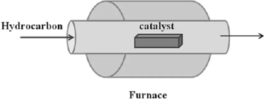
deposition of thin films of various materials. The deposition is made from precursors in the gas phase which adsorb on the target surface producing a condensed phase of a specific material. The attractiveness of the generation of graphene by CVD is based on the fact that this technique allows for scalability as well as low cost. A schematic experimental set-up is shown in Figure III.4. The process begins with an atomically flat surface of a transition metal substrate and an appropriate carbon precursor (like in methane or ethylene). The metal substrate plays the role of catalyst. This substrate is placed in a heated furnace and is attached to a gas delivery system. The precursor molecules will be brought into contact with the substrate surface from the gas phase or from liquid phase at elevated temperature. Upon contact with the surface, the precursor molecules are cracked to form carbon atoms and form gas-phase species, leaving the carbon atoms (which are free of functionalities) attached to the substrate surface. Graphene is formed when carbon atoms after diffusion on the metal surface, encounter other carbon atoms and form bonds.
Optimization of this process over the years has triggered interest in growth of graphene on relatively inexpensive polycrystalline Ni “Kim et al. (2009)”, “Obraztsov et al. (2007)”, “Reina et al. (2009)” and Cu “Li et al. (2009)”. substrates.
Figure I.7 Scheme of the growth process for the synthesis of graphene using CVD
Transfer of graphene grown on metals
Bae et al. “Bae et al. (2010)”, in 2010, first reported the transfer of single layer graphene (SLG) and few layer graphene (FLG) grown on Ni, by depositing a PMMA sacrificial layer and subsequently etching the underlying Ni by aqueous HCl solution “Bae et al. (2010)”. Li et al. transferred films grown by CVD on Cu, etched by iron nitrate “Li et al. (2009)”. Kim et al. introduced etching by aqueous FeCl3 in order to remove Ni without producing hydrogen bubbles, which may damage graphene when acid etching is used “Kim et al. (2009)”.
They also reported a technique where PDMS stamps are attached directly to the graphene surface. Ni is then chemically etched by FeCl3 leaving graphene attached to the Polydimethylsiloxane (PDMS). Graphene is then transferred to SiO2 by pressing and peeling the PDMS stamp. Bae et al. “Bae et al. (2010)” also introduced roll-to-roll transfer of graphene grown by CVD on Cu foils as large as 30 x 30in2, guided through a series of rolls: a thermal release tape was attached to the Cu+graphene foil, and then an etchant, an aqueous 0.1 M ammonium persulphate solution (NH4)2S2O8, removed Cu (Fugure III.5).
The tape+graphene film was then attached to a (flexible) target substrate and the supporting tape removed by heating, thus releasing graphene onto the target substrate “Bae et al. (2010)”.
To avoid Fe contamination caused by FeCl3 etching, ammonium persulfate [(NH4)2S2O8] was used “Aleman et al. (2010)”. To avoid mechanical defects caused by roll to roll transfer, a hot pressing process was developed “Kang et al. (2012)”: similar to a roll-to-roll process, the Cu+graphene foil is first attached to thermal release tape and then Cu is chemically etched. The tape+graphene foil is then placed on the target substrate and both are subsequently inserted between two hot metal plates with controlled T and pressure. This results in the detachment of the adhesive tape with very low
Figure I.8 Scheme of the graphene transfer process to a substrate “Bae et al.(2010)”
Figure I.9 Scheme of roll-to-roll process for the transfer of FLG from Ni foil to EVA/PET substrates “Juang et al. (2010)”
frictional stress, therefore less defects, than a roll-to-roll process “Kang et al. (2012)”.
According to Juang et al. “Juang et al. (2010)” roll-to-roll process is an ideal production choice when a very low cost per unit area of deposition is required. In the process for the transfer of few layer graphene to various flexible substrates, shown in Figure III.6, commercial ethylene-vinyl acetate copolymer (EVA) coated transparent polyethylene terephthalate (PET) sheets were used as the target substrate.
At a temperature of 150°C, the EVA/PET and FLG/Ni sheets were pressed together with hot rollers to form a double-sided PET/EVA/FLG/Ni sheet. The EVA layer here plays a role of viscose between the PET and FLG. After the hot rolling step, the sheet was passed onto cold rollers at room
temperature. The purpose of the cold rolling step is to separate the PET/EVA/FLG layers from the Ni surface in a uniform manner with a controlled, constant rolling speed
Multi-Walled Carbon Nanotubes
Arc discharge and Laser ablation
Arc discharge and laser ablation methods for growth of nanotubes have been actively pursued in the past ten years. Both methods involve the condensation of carbon atoms generated from evaporation of solid carbon sources. The temperature involved in these methods are close to the melting point of graphite, 3000-4000°C.
Arc discharge
In the arc discharge carbon atoms are evaporated by plasma of helium gas ignited by high currents passed through opposing carbon anode and cathode (Fig. I.1). Carbon nanotubes can be obtained by controlling the growth conditions such as the pressure of inert gas in the discharge chamber and the arcing current.
In 1992, a breakthrough in MWNTs growth by arc-discharge was first made by Ebbesen and Ajayan “Ebbesen et al. (1992)” who achieved growth and purification of high quality MWNTs. The syntheses were conducted in helium flow in the range of 2-3 atm, considerably higher than the pressure of gas used in the production of fullerene. A current of 60 - 100 A across a potential drop of about 25 V gives high yields of carbon nanotubes. The synthesised MWNTs have lengths on the order of ten microns and diameters in the range 5-30 nm. The nanotubes are typically bound together by strong van der Walls interactions and form tight bundles. MWNTs produced by arc-discharge are very straight, indicative of their high crystallinity. For as grown materials, there are few defects such as pentagons or heptagons existing on the sidewalls of nanotubes.
In the arc-discharge growth process the product contains carbon nanotubes and also others carbon species mainly constituted by multi-layered graphitic particles in polyhedron shapes. Purification of the tubes can be achieved by heating the as grown material in an oxygen environment to oxidise away the graphitic particles “Ebbesen end Ajayan (1992)”. The polyhedral graphitic particles exhibit higher oxidation rate than MWNTs; nevertheless, the oxidation purification process also removes an appreciable amount of nanotubes. A typical example of nanotubes so obtained is shown in Fig. I.2.
Figure I.11 TEM image of carbon nanotubes produced by arc discharge
Plasma arc Jet
Carbon nanotubes have been produced also by plasma arc jets “Hatta and Murata (1994)”, and in large quantities, by optimizing the quenching process in an arc between a graphite anode and a cooled copper electrode “Colbert et al. (1994)”. The product of these processes is a mixture of carbon nanotubes with different percents of amorphous carbon, fullerene. The tubes, so produced, are straight and show a small amount of structural defects.
Laser ablation
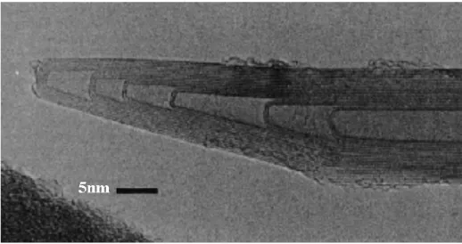
Laser ablation technique (Fig. I.3) is able to produce carbon nanotubes with the highest degree of purity. The method utilised intense laser pulses to ablate a carbon target containing a percent of nickel and/or cobalt. The target was placed in a tube-furnace heated to 1200°C. During laser ablation, a flow of inert gas was passed through the growth chamber to carry the grown nanotubes downstream to be collected on a cold finger. In contrast to the arc method, direct vaporisation allows far greater control over growth conditions, permits continuous operation, and produces nanotubes in higher yield and better quality.
By vaporisation of graphite rod with the addition of Co or Ni, it is possible to obtain materials containing until 80% of pure SWNTs with the same diameter “Guo et al. (1995), Thess et al. (1996)”, see Fig. I.4.
Figure I.12 Laser ablation schematic experimental setup
Chemical Vapour deposition (CVD)
One more effective method of generating carbon nanotubes is based on the chemical vapour deposition (CVD) of hydrocarbons over supported transition metal particles, that constitute the active species.
Figure I.13 TEM images of carbon nanotubes produced by laser ablation method (a); tube wall particular (b).
This is a successful way to synthesize carbon nanotubes, because of the lower growth temperature (below 1000°C) compared to arc-discharge or laser vaporization methods and of the possibility to control inner diameter and length of the tubes.
Figure I.14 CVD schematic experimental setup
The growth process involves heating a catalyst material to high temperatures in a tube furnace and flowing a hydrocarbon vapour through the tube reactor for a period of time. Materials grown over the catalyst are collected upon cooling the system to room temperature.
The general nanotube growth mechanism in a CVD process (see Chapter IV), involves the dissociation of hydrocarbon molecules catalysed by a transition metal, and the dissolution and saturation of carbon atoms in the metal nanoparticles. The precipitation of carbon from the saturated metal leads to the formation of tubular carbon solids in sp2 structure. Tubule formation is favoured over other forms of carbon such as graphitic sheets with open edges. This is because a tube contains no dangling bonds and therefore is in a low energy form.
The key parameters in nanotube CVD growth are the nature of hydrocarbon and catalyst and the reaction temperature.
For MWNT growth, most of the CVD methods employ ethylene or acetylene as carbon feedstock and the growth temperature is typically in the range of 550-750°C “Ivanov et al. (1994), B.Nagy et al. (2000b), Hernadi et al. (1996)”.
The catalytic system consists of transition metals, such as Fe, Ni, Cu and Co of several nanometers in size, used as catalysts, dispersed on a support constituted in general of metal oxides, but in some cases of zeolites.
The presence of transition metal particles is essential for the formation of nanotubes by the pyrolysis process. It has been suggested that the nanotube diameter is determined by the size of the metal particles “Rodriguez (1993)”.
The length of nanotubes varies from several micrometers to several tens of micrometers.
The rationale for choosing these metals as catalyst for CVD growth of nanotubes lies in the phase diagram of the system metal-carbon.
At high temperature carbon has finite solubility in these metals, which leads to the formation of metal-carbon solutions (see Chapter IV). Iron,
cobalt and nickel are the favoured catalytic metals in laser ablation and arc-discharge too.
This simple fact may hint that laser, arc and CVD growth methods may share a common nanotubes growth mechanism, although very different approaches are used to provide carbon feedstock.
The CVD method permitting to generate the nanotubes in a wide range of their physical characteristics was gathering force in the set of works “Yacaman et al. (1993), Ivanov et al. (1994), B.Nagy et al. (2000b), Hernadi et al. (1996)”.
However, these syntheses gave rise, together with carbon nanotubes, to different carbon structures, mostly amorphous generated in the support porosity or coating the outside surface of carbon nanotubes. Therefore, different methods for purification, consisting essentially in thermal and chemical oxidations, have been studied. For example, amorphous carbon can be burned away by heating the nanotubes in air “Shi at al. (1999b)”.
The yield of nanotubes in a sample depends on the type of catalyst: in the presence of iron, for example, it is much higher than for cobalt. For copper catalyst a great part of carbon precipitates in an amorphous form “Chesnokov et al. (1994)”.
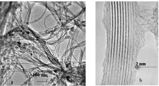
The typical appearance is a tangle of tubes that after sonication exhibit the aspect shown in Fig. I.6.
Recent interest in CVD nanotube is also due to the idea that aligned and ordered nanotube structures can be grown on surface with a control that is not possible with arc-discharge or laser ablation techniques “Dai et al. (1999)”.
Methods that have been developed to obtain aligned MWNTs include CVD growth of nanotubes in the pores of mesoporous silica, an approach developed by Xie’s group at the Chinese Academy of Science. The catalyst used in this case is iron oxide particles formed inside the pores of silica. The carbon feedstock is 9% acetylene in nitrogen at 180 torr pressure, and the growth temperature is 600°C. Remarkably, nanotubes with lengths up to millimetres are obtained “Li et al. (1996)”.
Ren has grown relatively large-diameter, well-aligned MWNTs, for field emission display application, forming oriented “forest” on glass substrate using a plasma assisted CVD method with nickel as catalyst and acetylene as carbon source around 660°C “Ren et al. (1998)”.
An extension of the method reported in “Li et al. (1996)” has produced self-oriented patterned arrays of CNTs on iron-coated porous silicon “Fan et al. (1999b)”.
Dai’s group has been devising growth strategies for ordered MWNTs architectures by CVD on catalytically patterned substrate. They have found that MWNTs can self-assemble into aligned structures as they grow, and the driving force for self-aligned is the van der Waals interaction between nanotubes “Dai et al. (2000)”. The growth approach involves catalyst patterning and rational design of the substrate to enhance catalyst-substrate interactions and control the catalyst particle size. Porous silicon is found to be an ideal substrate for this approach and can be obtained by electrochemical etching of n-type silicon wafers in hydrofluoric acid/methanol solution. The resulting substrate consists of a thin nanoporous layer on the top of a macroporous layer.
The porous silicon substrate exhibit important advantages over plain silicon substrate in the synthesis of self-aligned nanotubes. Growth on substrates containing both porous silicon and plain silicon portions permits to obtain higher rate grow of nanotubes (in terms of length/min), than on porous substrate. This suggest that ethylene molecules can permeate through the macroporous silicon layer and thus efficiently feed the growth of nanotubes within the towers (Fig. I.7).
Ren et al. “Ren et al. (1998)” employed plasma-enhanced CVD on nickel-coated glass with acetylene and ammonia mixtures for this purpose. The mechanism of growth of nanotubes by this method and the exact role of the metal particles was investigated, a nucleation process involving the metal particles is considered to be important.
Fan et al. “Fan et al. (1999a)” have obtained aligned nanotubes by employing catalytic decomposition on porous silicon and plain silicon substrates patterned with iron films. Also in this case, the role of the metal particles is not completely known.
The role of the transition metal particles assumes importance in view of the report of Pan et al. “Pan et al. (1999)” that aligned nanotubes can be obtained by pyrolysis of acetylene over iron/silica catalytic surfaces.
In the light of the earlier work on the synthesis of carbon nanotubes by pyrolysis of mixtures of organometallic precursors and hydrocarbons, “Sen et al. (1997a, 1997b)” one would expect that the transition metal nanoparticles produced in situ in the pyrolysis may not only nucleate the formation of carbon nanotubes but also align them.
Figure I.16 Schematic diagram of the growth process
This aspect has been examined by carrying out the pyrolysis of metallocenes along with additional hydrocarbon sources in a suitably designed apparatus “Sen et al. (1997a, 1997b), Satishcumar et al. (1999), Rao et al. (1998b)”. Scanning electron microscopy (SEM) images of aligned nanotubes obtained by pyrolysis of ferrocene are shown in Fig. I.8. Images a) and b) show views of the aligned nanotubes along and perpendicular to the axis of the nanotubes, respectively. Figure I.7a shows the top view of the aligned nanotubes, wherein the nanotube tips are seen, while the image in Figure I.7b shows the side view. The average length of these nanotubes is generally around 60 mm obtained either form methane and acetylene.
Recently, CVD conducted in the presence of inorganic structure-directed or templated structure have been explored to synthesize a wide variety of new carbon materials. During templated synthesis methods, substrate or precursor materials are included into the template framework in such a way that their final structure reflects shape and dimension of the templates.
Organic templates are commonly used to synthesize inorganic materials. For example, surfactants have been used to template the synthesis of MCM-41 “Asefa et al. (1999)”, or other porous silicates “Sandi et al. (1999), Kresge et al. (1992)” and oxides “Bagshaw et al. (1995)”.
Figure I.17 SEM images of aligned carbon nanotubes obtained by the pyrolysis of ferrocene, images a) and b) show views of the aligned nanotubes along and perpendicular to the axis of the nanotubes respectively
In the templated synthesis method carbon nanotubes are obtained as a print of a directional structure. In this case addition of metal particles to the system is not necessary. It can lead to the production of aligned carbon nanotubes.
A major hurdle in applying CVD to template synthesis is the necessity to control the deposition rate. In fact, the pores can become blocked before the chemical vapour traverse the length of the pores.
First example of carbon nanotubes synthesis by CVD template-based method has been reported by Martin et al. “Hulteen and Martin (1997), Che et al. (1998)”, using alumina membrane, with and without the additon of transition metal catalysts.
The use of micoporous zeolites, such as Y, ZSM-5, mordenite, L, as templates “Kyotani et al. (2003)”, and only recently BEA, has been investigated. By propylene CVD carbon materials with a controlled microporosity have been obtained.
Single-Walled Carbon Nanotubes
The nanotubes obtained by the previously described methods are generally MWNTs having several graphitic sheets or layers. SWNTs can be also synthesised by using these methods.
For a long time, arc-discharge and laser–ablation have been the principal methods for obtaining nearly perfect SWNTs. Both methods are based on evaporating carbon atoms from solid carbon sources at about 3000°C, which is not efficient and limits the scale-up of SWNTs production. Recently, growth of SWNTs with structural perfection was achieved by CVD methods. SWNTs have been first prepared by metal-catalysed direct-current arcing of graphite rods “Ichihashi and Iijima (1993), Bethune et al. (1993)” under helium atmosphere. The graphite anode was filled with metal powders (Fe, Co, Ni) and the cathode was pure graphite. SWNTs generally occur in the weblike material deposited behind the cathode. Various metal catalysts have been used to make SWNTs by this route.
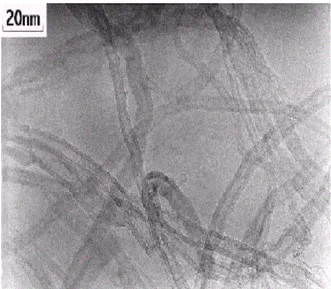
Arc evaporation of graphite rods filled with nickel and yttrium under a helium atmosphere (660 Torr) gives rise to weblike deposits on the chamber walls near the cathode, which consist of SWNT bundles “Rao et al. (1998a)”. HRTEM images show bundles consisting of 10 - 50 SWNTs forming highway junctions (Figure I.9). The average diameter of the SWNTs was around 1.4 nm and the length extended up to 10 mm.
SWNTs have been produced in more than 70% yield by the condensation of a laser-vaporized carbon - nickel - cobalt mixture at 1200°C “Thess et al. (1996)”. These SWNTs were nearly uniform in diameter and self-assembled into ropes which consists of 100 to 500 tubes in a 2D triangular lattice.
Figure I.18 HRTEM image of SWNTs obtained by arcing graphite electrodes
Cassel et al. (1999) found that by using methane as carbon source reaction temperatures in the range of 850-1000 °C, suitable catalyst materials and flow conditions, one can grow high quality SWNT materials by simple CVD process. High temperature is necessary to form SWNTs that have small diameters and thus high strain energies, and allow for nearly-defect free crystalline nanotubes structures. Among all hydrocarbon molecules, methane is the most stable at high temperatures against self-decomposition. Therefore, catalytic decomposition of methane by transition-metal catalyst particles is the dominant process in SWNT growth. The choice of carbon feedstock is one of the key elements to the growth of high quality SWNTs containing no defects and amorphous carbon over-coating.
Another CVD approach to SWNTs was reported by Smalley and coworkers who used ethylene as carbon feedstock and growth temperature around 800°C “Hafner et al. (1998)”. In this case, low partial pressure ethylene was employed in order to reduce amorphous carbon formation due to self-pyrolysis/dissociatin of ethylene at high growth temperature.
Gaining an understanding of the chemistry involved in the catalyst and nanotube growth process is critical to enable materials production scale-up by CVD. The choice of many parameters in CVD requires to be rationalised in order to optimise the materials growth. Within the methane CVD approach for SWNT growth, it has been found high yield and quality SWNTs “Cassel at al. (1999)”. Cassel at al. have developed a catalyst consisting of Fe/Mo bimetallic species supported on a sol-gel derived
alumina-silica multicomponent material. The catalyst exhibits a surface are of approximately 200 m2/g and mesopore volume of 0.8 mL/g.
B.Nagy et al. “ Colomer et al. (2000)” obtained SWNTs in high yield by the decomposition of methane over transition-metal-supported MgO substrates.
Different catalysts have been prepared by impregnation of MgO with ethanol solution of metal salts (Co, Ni, Fe) or a mixture of metal salts (Co-Fe) in the appropriate concentration. The used carbon source methane/hydrogen has been feed at 1000°C obtaining SWNTs with a diameter in the range 0.8-2 nm. The high resolution TEM imaging of he SWNTs synthesized by this method frequently shows closed tube ends free of encapsulated metal particles as observeed in Fig. I.10. The opposite ends were typically found embedded in the catalyst support particles, suggesting a base-growth process.
Figure I.19 HRTEM image of the ends of SWNTS
Considering the importance of the SWNTs, alternate synthesis strategies have been explored. Under controlled conditions of pyrolysis, dilute hydrocarbon - organometallic mixtures yield SWNTs “Satishkumar et al. (1998), Rao et al. (1998)”.
Pyrolysis of a nickelocene - acetylene mixture at 1100 °C yields SWNTs, shown in TEM images in Figure I.11 “Satishkumar et al. (1998)”. The diameter of the SWNT in Figure I.11a is 1.4 nm. It may be recalled that the pyrolysis of nickelocene mixed to benzene under similar conditions primarily yields MWNTs. Acetylene appears to be a better carbon source for the preparation of SWNTs, since it contains a smaller number of carbon
atoms per molecule. The bottom portion of the SWNT in Figure I.11b shows amorphous carbon coating around the tube. Many of the SWNT preparations show the presence of amorphous carbon. This can be avoided by reducing the concentration of hydrocarbon (C2H2) and mixing hydrogen in the argon stream.
Pyrolysis of acetylene in mixture with [Fe(CO)5] at 1100 °C gives good yields of SWNTs (Figure I.12). Table I.1 summarizes the nature of products obtained by pyrolysis of hydrocarbon - organometallic mixtures at 1100°C in a stream of argon and hydrogen.
Pyrolysis of ferrocene - thiophene mixtures also yield SWNTs but the yield appears to be somewhat low. Pyrolysis of benzene and thiophene along with ferrocene gives a high yield of SWNTs “Cheng, H. M. et al. (1998)”.
Figure I.20 HRTEM image of SWNTs obtained by the pyrolysis of nickelocene and C2H2. (flow rate= 50cm3/min) at 1100°C in a flow Ar (1000
cm3/min)
Laplaze et al. have demonstrated that concentrated solar energy can be employed to vaporize graphite to synthesize SWNTs “Laplaze et al. (1998)”. Dai et al. have prepared SWNTs by the disproportionation of CO at 1200°C over molybdenum particles of a few nanometers diameter dispersed in a fumed alumina matrix “Dai et al. (1996)”.
Nikolaev et al. have obtained SWNTs using a gas-phase catalytic method involving the pyrolysis of [Fe(CO)5] and CO “Nikolaev et al. (1999)”. The