OVERVIEW ON NEW HIGH VOLTAGE PULSE
MODULATORS IN THE RF POWER SYSTEMS
VINCENZO SURRENTI
Fusion and Technology for Nuclear Safety and Security Department Division of Technology Applications for Security,Health and Heritage Development Laboratory of Particle Accelerators and MedicalApplications FrascatiResearch Centre,Rome
RT/2017/30/ENEA
ITALIAN NATIONAL AGENCY FOR NEW TECHNOLOGIES, ENERGY AND SUSTAINABLE ECONOMIC DEVELOPMENT
VINCENZO SURRENTI Fusion and Technology for Nuclear Safety and Security Department Division of Technology Applications for Security, Health and Heritage Development Laboratory of Particle Accelerators and Medical Applications Frascati Research Centre, Rome
OVERVIEW ON NEW HIGH VOLTAGE PULSE
MODULATORS IN THE RF POWER SYSTEMS
RT/2017/30/ENEA
ITALIAN NATIONAL AGENCY FOR NEW TECHNOLOGIES, ENERGY AND SUSTAINABLE ECONOMIC DEVELOPMENT
I rapporti tecnici sono scaricabili in formato pdf dal sito web ENEA alla pagina http://www.enea.it/it/produzione-scientifica/rapporti-tecnici
I contenuti tecnico-scientifici dei rapporti tecnici dell’ENEA rispecchiano l’opinione degli autori e non necessariamente quella dell’Agenzia
The technical and scientific contents of these reports express the opinion of the authors but not necessarily the opinion of ENEA.
OVERVIEW ON NEW HIGH VOLTAGE PULSE MODULATORS IN THE RF POWER SYSTEMS Vincenzo Surrenti
Abstract
Over the last 50 years, the technology of high voltage pulse modulators has undergone remarkable improvements thanks to the use of new semiconductor devices, high integration control systems and the implementation of multicore pulse transformers designed by numerical methods (FEM computing, method of image charges, image current method).
The main advantages of these technological innovations have resulted in: - Power systems with efficiencies of up to 99%;
- Impulsive output responses with lower rise time and droop voltage;
- Increasing output voltages to be able to power radiofrequency tube devices capable of deli-vering better performance in terms of frequency response, power and efficiency.
These pulse modulators, once used in limited applications (radar systems, industrial radiofrequency systems), are today used in a wide variety of industrial, medical and research applications, particularly where reliability, stability and versatility are required, thanks to increased performance and to reduced manufacturing costs.
This report will first describe the schemes that are mainly used in the implementation of new pulse modulators and then will be focused on high-voltage modulators based on a pulse transformer. Then, the general block diagram of the above mentioned modulator type will be illustrated and the pecu-liarities of each subsystem will be described indicating the technological solutions to be used to im-prove the performances.
Key words: Power electronics, Solid state modulator, Pulse transformers, Pulse modulation, Pulse circuits, Transformer cores, Pulse power systems, Pulse generation, Pulsed RF power, Klystron-mo-dulator RF power system.
Riassunto
Negli ultimi 50 anni, la tecnologia costruttiva dei modulatori impulsivi ad alta tensione ha subito no-tevoli migliorie grazie all’impiego di nuovi dispositivi a semiconduttore, sistemi di controllo ad alta in-tegrazione ed alla realizzazione di trasformatori d’impulso multicore progettati mediante l’ausilio di metodi numerici (FEM computing, metodo delle cariche immagine, metodo delle correnti immagine). I principali vantaggi ottenuti da queste innovazioni tecnologiche hanno permesso di ottenere: - sistemi di potenza con efficienze prossime al 99%,
- risposte impulsive in uscita con minori rise time e droop voltage,
- tensioni d’uscita sempre più elevate per poter alimentare dispositivi a tubo per radiofrequenza capaci di fornire prestazioni migliori in termini di risposta in frequenza, potenza ed efficienza.
Questi modulatori impulsivi, che un tempo trovavano impiego in limitate applicazioni (impianti radar, impianti a radio frequenza in campo industriale), oggi vengono impiegati grazie all’incremento delle loro prestazioni ed alla riduzione dei costi in svariate applicazioni industriali, medicali e di ricerca so-prattutto laddove è richiesta affidabilità, stabilità e versatilità di funzionamento.
Nel presente rapporto descriveremo preliminarmente quali sono gli schemi prevalentemente impiegati nella realizzazione dei nuovi modulatori impulsivi per concentrare l’attenzione sui modulatori ad alta tensione basati su un trasformatore d’impulso. Quindi verrà illustrato lo schema blocchi generale del suddetto tipo di modulatore descrivendone le peculiarità di ciascun sottosistema e indicando le solu-zioni tecnologiche adottate per migliorarne le prestasolu-zioni.
Parole chiave: Elettronica di potenza, Modulatori a stato solido, Trasformatori d’impulso, Circuiti impulsivi, Sistemi di potenza impulsivi, Generatori d’impulsi, Potenza RF impulsata, Sistemi di po-tenza per modulatori RF.
1 Introduction
2 State of the art of the solid state High Voltage Modulator 3 Topological scheme of the solid state High Voltage Modulator 4 Distribution network
5 PFC and level tranformer 6 Charging unit
6.1 DC/DC boost converter
6.1.1 Series Connection of Switches 6.1.2 Converter Control
7 Pulse generator
7.1 Switches and driver circuits in the pulse generator 7.2 IGBT Driver [6]
7.2.1 Double stage turn on
7.2.2 Double stage turn off and voltage clamping 7.2.3 Short-Circuit Detection
7.2.4 Control Signal of the IGBT driver unit 7.3 Active premagnetization
7.4 Inductor Bouncer circuit 8 Pulse transformer
8.1 Pulse shape design
8.2 Electro-mechanical design 9 Conclusion 10 Acknowledgments 11 References 7 8 10 12 13 24 25 28 28 31 35 36 38 40 42 45 48 52 58 58 62 73 73 73
INDEX
7 1 Introduction
In radiofrequency (RF) power plants, the RF signal can be directly generated by a power source or amplified by a low power seed.
In both cases, the power plant involves the use of a tube device, which has the following common elements: - An electron gun or cathode,
- A collector or anode where accelerated electrons are collected.
In the first case, the sources are constituted by tube devices that can generate from the background noise and self-sustaining the natural oscillations for which the tube has been realized. The magnetron, the gyrotron, the CARM belong to this class of devices.
In the second case, the tube device, by means of an electron beam velocity modulation mechanism produced by the gun, is capable of amplifying a RF signal. The klystron and the traveling wave tube belong to this class of devices.
There are also other types of power tube devices that are used in radiofrequency power plants, as amplifiers, that amplify a source RF signal by means of a current modulation mechanism. The planar triode, the pentode, the tetrode and the inductive output tube belong to this class of devices.
All these devices in order to be able to operate impulsively must be powered by a pulse modulator. There are many applications where it is required the use of RF sources operating impulsively for industrial, medical and research. However, every type of application is characterized by a particular power and pulse duration. In the case of industrial use these systems can feed:
- radar installations,
- radiofrequency ovens,
- radiographic equipment,
- sterilization systems for radiofrequency and accelerated electrons,
and it is therefore important that the pulse modulator has the highest efficiency and the greater power. In the case of medical use, these systems can feed:
- radiogenic sources,
- source for the production of radiotherapy drugs, - hadron-therapy machines
and in this case, the pulse modulator requires a stable response in terms of rising time and droop voltage. Finally, in the case of use in research facilities, these modulators can feed for example:
- long linear colliders, - nuclear fusion devices.
8
The demand for the pulse modulator in this case is twofold, i.e. it is necessary to ensure stable responses and an overall efficient system. In this report, new types of pulse modulators for RF devices will be examined, mainly made with solid-state switching devices.
2 State of the art of the solid state High Voltage Modulator
In the last 50 years the development of modern high-voltage modulators has changed considerably, basically thanks to the progress made in the following areas:
- integration of programmable devices such as ARM, FPGA, etc.
- development of new power solid-state devices that can operate with maximum operating voltages around the thousand volts and rated currents around the thousand amperes.
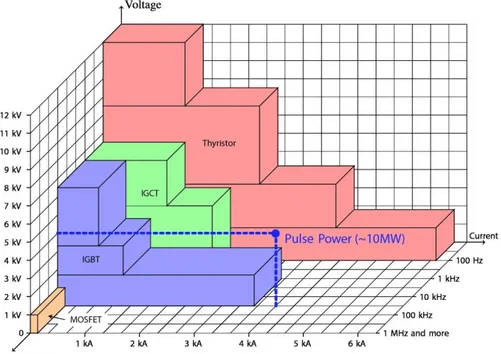
This progress have led to a change in state of the art of modern High-Voltage Modulators. Today modern high voltage modulators are to be classified according to the following two parameters: pulse length and used power. In fact, in function of the above parameters they find a very precise application as is illustrated in Fig. 1.
According to the classification shown in the Fig. 1 and according to the construction technology the modern solid state high voltage pulse modulators can be divided into the following three large families:
Short pulse modulator, Mid-range pulse modulator, Long pulse modulator.
9 Fig. 2 shown today's operating limits of the solid state devices used in the production of modern pulse modulators. The above graph justifies the use of Thyristors and IGCTs in long pulse modulator and the use of IGBTs and MOSFETs in the mid-range and short pulse modulator. However, the use of this last type of devices in large power plants involves the use of more complex and expensive circuit configurations to overcome the limited operating range in voltage and current.
In design phase of high voltage pulse modulators, it is necessary to reduce the operating voltage of the electronic devices used as switches with respect to what is indicated by the manufacturer to increase the mean time to failure; this reduction in the operating voltage should be weighted according to the height of installation of the system. Indeed, in these devices that operate for long intervals of time in reverse bias, the avalanche breakdown phenomenon as result of swarms of cosmic rays in the reverse bias region becomes all the more probable, the higher is the working height of the plant and the more extended is the reverse region (that is, the higher the reverse bias voltage). Reducing the operating voltage of the switch involves their use in chains connected in series and in the design phase it is necessary that particular attention is made to the interconnection and command mode to avoid extra-tension in the opening phase.
Another requirement to be met, in case it is wanted to realize a pulse modulator which operates at high power, the switching devices must be connected in parallel so as to respect the current operating limits. Today most of the pulse modulators, to improve the conversion efficiency of the switching devices, are controlled by suitable drivers operating in boundary conduction mode (BCM). In this way the inductive current controlled by the switching device flows in a discontinuous mode, the main benefit is a reduction in
10
the magnetic energy stored by the inductor or transformer with a consequent reduction in the size, weight and power losses of the latter.
3 Topological scheme of the solid state High Voltage Modulator
There are two possible realization for a solid-state modulator, a Marx generator and a pulse-transformer-based solution.
The Marx generator (cfc. Fig. 3) is based on the principle of charging capacitors in parallel for a period and, in a subsequent period, to connect the capacitors in series to create a higher voltage. The classical Marx generator uses spark gaps to connect capacitors in series and to create a single high-voltage pulse. Nowadays, modern topologies based on the same principle can be realized with solid-states switches. The modularity of this type of converter allows to make connections in series and in parallel between modules in order to meet all requirements in terms of voltage and current which also show a high level of reliability, availability and maintainability. The main disadvantage of this type of modulator is the high energy level stored, by requiring costly systems for safe disposal in case of short circuit (electro-optic circuit devices for electrostatic decoupling of the electronic drive circuit of the switches). Just for the abovementioned disadvantages, this type of converter is adopted to realize steady-state converters dc-dc or long pulse modulator.
In a pulse-transformer based modulators, thanks to the use of a transformer the switches can be operated at a lower voltage. In addition, less switches are required, because there is no series connection necessary to achieve the output voltage.
Pulse-transformer-based modulators can be divided into three different categories: - transformers with a single core,
- transformers with multiple cores, - and transmission-line transformers.
A single-core transformer consists of one magnetic core and two or more windings. Transformers with multiple cores are realized in different configurations. The simplest solution is connecting multiple transformers in series or in parallel. A parallel connection of multiple pulse transformers does not result in
a) b)
Fig. 3 Different type of Marx generator:
11 any benefit compared with a solution, where multiple switches are connected in parallel on the primary side of a single-core transformer. Connecting multiple transformers in series is more useful. The current on the primary side is given by the current on the secondary side and the turns ratio. Therefore the series connection guarantees equal currents on the secondary side of all transformers, resulting in equal currents on the primary side if the transformers have the same turns ratio. The load current is equally shared between the semiconductor switches.
The series connection of multiple transformers can be improved by enclosing all cores with one secondary winding, instead of an individual secondary winding for each core.
The third possible structure is a transmission-line transformer. In such transformers, multiple transmission lines are connected to a common source at one end and in series at the other end of the line [4]. These types of structure are referred to as ‘‘ line-type” pulsers because the energy-storage device is essentially a lumped-constant transmission line. Since this component of the line type pulser serves not only as the source of electrical energy during the pulse but also as the pulse-shaping element, it has become commonly known as a “ pulse-forming network,” PFN. There are essentially two classes of pulse-forming networks, namely, those in which the energy for the pulse is stored in an electrostatic field in the amount 12𝐶𝑉2 and those in which this energy is in a magnetic field in the amount 12𝐿𝐼2. Often, coaxial cables are used as transmission lines. To
improve the low-frequency response, the cables are wound around a magnetic core. Other times the lumped-constant transmission line consist of inductances and condensers which may be put together in any one of a number of possible configurations. The configuration chosen for the particular purpose at hand depends on the ease with which the network can be fabricated, as well as on the specific pulse characteristic desired. Anyway, it is realized the transmission line, the impedance must be matched to the load impedance for maximum power transfer. The main disadvantage of this type of modulators is the setup of the forming network in accord to the applied load.
Among the described modulators the most diffused in the construction of high voltage pulse generator with pulses of duration up to the millisecond is the pulse modulator based on the transformer in the version in single or multiple magnetic cores. Its development is due to the ease with which its design can be adapted to any type of RF source or load.
The general layout of a high voltage pulse transformer-based modulator consists of the following subsystems:
a galvanically isolated ac/dc converter with a Power Factor Correction (PFC) a Charging Unit
a Primary Bank of energy storage
one or more Pulse Generator (included the pulse transformer) a possible Bouncer subsystem
12
The following paragraphs have been divided for each subsystem in order to motivate their use, describe the principle of operation, indicating the upgrades that have improved efficiency, and that have allowed their use even when the design specifications are difficult to meet.
4 Distribution network
The preliminary study of the feasibility of a pulse modulator object of the present documents contemplate its insertion in an electrical distribution system, subject to the Italian laws. In particular, the point of access to the electricity distribution network is constituted by a secondary substation supplied in MV (Medium Voltage), provided with at least a MV / LV (Low Voltage) transformer dedicated to the distribution network (law’s norms CEI 0-16 art. 3.2, CEI 0-21 art. 3.2, CEI 64-8/2 art. 21.8). The MV / LV transformer of that distribution station is generally made up of a three-phase transformer with internal Y connection and the following conversion ratio 20kV / 400V.
The type of the neutral connection and the grounds connection to be taken into consideration is that of a TN-S system. For this type of system it is provided the separate use of neutral and protection conductors, therefore the security is related to the efficiency of the neutral and ground network.
It must be remembered that the legislative norms for TN systems contemplate a different type of protective devices for the direct cables contact and for indirect contact. In fact, in the first case it is provided the use of devices that monitor the maximum operating current of the plant and which ensures a inversely proportional to the contact current intervention time. For indirect contacts is contemplated instead the realization of the ground systems that consist of sinks, ground conductors and equipotential conductors and a system which monitors the current difference between the phase current and the neutral current.
AC DC DC DC
13 This premise is essential in the choice of design as it will ensure the integration of the system into the electrical distribution network, making it easier to design the diagnostic system for detecting plant failures and operations to be used to protect the plant.
5 PFC and level tranformer
The first subsystem that will be described is the Power Factor Correction (PFC). The PFC performs the following tasks:
- to correct the power factor shown by the modulator to the power grid,
- uncouple galvanically the charge unit from the main distribution network,
- to provide an adequate output voltage to the pulse generator.
In Fig. 5 is shown a typical layout where it is possible identify the following subsystem:
- An AC / DC converter: that in addition to providing a continuous output voltage will allow to correct the power factor shown to the distribution network.
- A DC/DC converter: consists in turn of two subsystems, a DC/AC converter and an AC/DC converter (full bridge type) galvanically decoupled by the transformer which also shifts the level of the PFC output voltage.
- An integrated control system that manages all the subsystems in order to reduce the Total Harmonic Distorsion (THD) of the current request to the distribution network, and provide the predetermined output voltage. Finally, the control system is able to handle the direction of the energy flow so that it can be recovered when the modulator is in standby mode or if it is necessary to handle a fault (load side).
Correct the power factor involves modifying the input current waveform of the power supplies in such a way that the distributor mains always provide a real power to the modulator. Another reason to employ PFC in many of today’s power supplies is to respect the legal requirements. Today, electrical equipment in Europe must comply with the IEC 61000-3-4 and IEC 61000-3-12 (limitation of harmonic currents injected
14
into the public supply system). This requirements specify the maximum amplitude of line-frequency harmonics up to and including the 39th harmonic.
In Tab. 1 and Tab. 2 is shown in tabular form the requirements for different types of equipment as a function of the short-circuit ratio (Rsce) or :
𝑅𝑠𝑐𝑒 𝑚𝑖𝑛= 𝑉 𝑍 ∙ 𝐼𝑒𝑞
where 𝑉 is the grid line voltage, 𝑍 is the supply output impedance and 𝐼𝑒𝑞 is the target line current. Power factor correction is simply defined as the ratio of real power to apparent power, or:
Tab. 1 IEC 61000-3-12 requirements for balanced three-phase equipment
15 Fig. 6 Input characteristics of a typical switched power supply
without PFC.
where the real power is the average, over a cycle, of the instantaneous product of current and voltage, and the apparent power is the product of the rms value of current per the rms value of voltage. If the load is composed of resistive, capacitive and inductive elements and all are linear (invariant with current and voltage). In the case which the current and voltage are sinusoidal and in phase (resistive load), the power factor is 1.0 while if both are sinusoidal but not in phase, the power factor is the cosine of the phase angle.
The solid state modulator present nonlinear impedance to the mains. The input circuit usually consists of a half-wave or full-wave rectifier followed by a storage capacitor. This latter elements is able to maintain approximately to the peak sinusoidal input voltage until the next peak will arrive to recharge the capacitor. In this case current is drawn from the input only at the peaks of the input waveform, and this pulse of current must contain enough energy to sustain the load until the next peak.
The current and voltage are perfectly in phase (Fig. 6) , in spite of the severe distortion of the current waveform. Applying the “cosine of the phase angle” definition would lead to the erroneous conclusion that this power supply has a power factor of 1.0.
However the harmonic content of the current waveform (Fig. 7) shows the presence of the even harmonics with not negligible amplitude. Since only the fundamental component produces real power, while the other harmonics contribute to the apparent power, the actual power factor is well below 1.0. This deviation is represented by a term called distortion factor and is primarily responsible for the non-unity power factor in switched power supply (SPS).
The general equation governing the relationship between the real power and apparent power is given by: < Pin> = V̂ Iin̂cos φcosθ in
16
where 𝐕̂ is the rms input voltage, 𝐈𝐢𝐧 ̂ is the rms input current, < 𝐏𝐢𝐧 𝐢𝐧 > is the real power expressed in Watt ,
𝐕̂ 𝐈𝐢𝐧̂ is the apparent power expressed in VA, 𝒄𝒐𝒔 𝝋 is the displacement factor coming from the phase 𝐢𝐧
angle φ between the voltage and current waveforms and 𝒄𝒐𝒔𝜽 is the distortion factor. Therefore it is preferred to define the power factor through the following relation:
𝑃𝐹 = 𝜆 = 1 √1+𝑇𝐻𝐷𝑖2𝑐𝑜𝑠𝜑 𝑇𝐻𝐷𝑖 = 100 ∙ √∑ 𝐼𝑝2 𝐼12 ∞ 𝑝=2
where with THDi denotes the total harmonic distortion of the input current to the power converter.
In the case of three-phase distribution networks, as always two diode at a time carry current to the converter except in the commutation interval, this means that the conduction angle at most will 60° at which correspond a relatively high low-frequency harmonic content or a THDi ≈ 30%.
In order to avoid voltage distortions resulting from voltage drops across the inner (inductive) mains impedance or the excitation of resonances in the distribution grid a THDi < 5% at rated power is often required.
This network quality can only be achieved with rectifier systems based by active power factor correction (PFC). A further important aspect of the use of active (PFC) rectifier systems is the possibility to control the output dc voltage to a constant value, independent of the actual mains voltage. A converter stage on the output side can be dimensioned to a narrow voltage range. The mains voltage range must be considered only for the dimensioning of the rectifier stage (the delivery of a given rated power, e.g., at half of the input voltage, leads to a doubling of the input current that must be handled by the power semiconductors, passive power components and the EMI filter).
Therefore the requirements placed on active PFC rectifier systems can be summarized as follows:
- sinusoidal input current according to regulations regarding the mains behavior of three-phase rectifier systems (EN 61000-3-2 if < 16 A, 61000-3-4 if > 16 A); in industry, however, typically independent of the concrete application, a THDi < 5% is required (at the rated operating point); - ohmic fundamental mains behavior ( cosφ > 0.99 );
- regulated output voltage; depending on the required level of the output dc voltage relative to the mains voltage, a system with boost-, buck-, or buck–boost-type characteristic has to be provided; - handling of a mains phase failure, i.e., for interruption of one mains phase, continued operation at
reduced power and unchanged sinusoidal current shape should be possible;
- unidirectional power flow, perhaps with (limited) capability of reactive power compensation;
- compliance with specifications regarding electromagnetic, especially conducted interference emissions by means of suitable EMI filtering.
An approximately sinusoidal mains current and/or partial elimination of low-frequency harmonics in the input current is only obtainable with multipulse systems, i.e., for 12-,18-, or 36-pulse rectifier circuits. This type of PFC is grouped in the class of Passive system.
17 Fig. 9 Schema of the Hybrid third harmonic current
injection-Active Filter Rectifier with the relative current distribution
Integrating the passive system with in cascade power devices that actively control the flow of power it is possible improve the control of the sinusoidal mains current and also adjust the output voltage within certain limits. Such type of PFC is classified as a Hybrid system.
Conversely, if the integration of the power semiconductors takes place inside of each leg of the bridge, the control of switching of these devices will be certainly more complex and therefore in this case the type of PFC will be grouped in the Active PFC system.
The choice of the particular type of PFC, depending on unavoidably from the point of view of the effectiveness in reducing the total harmonic distortion of the input current and in the regulation capability of the output voltage, furthermore it depends on the circuital and control complexity and consequently by the cost of implementation.
The best type of PFC is a particular Active PFC system called Hybrid third harmonic current injection-Active Filter Rectifier.
This latter is a variant of the boost-type PFC rectifier that over obtain a limited regulation of the output voltage shows good performance from the point of view of the harmonic distortion of the input current.
In fact, the boost-type PFC rectifier (chain in cascade of two stage: three-phase bridge and a boost-converter dc-dc) is capable to providing a harmonic distortion of input current not less than 30%.
In Fig. 9 is shown the basic configuration of the conventional current injection topology for a three-phase diode rectifier that fed a load.
It consists of two stages. The first stage is a six-pulse, diode-bridge rectifier. The second stage consists of two step-up dc-dc (boost) converters which modulate the current in the dc-link to be ( Id + i3) and (Id - i3).
Fig. 8 Three-phase extension of the boost type PFC : a) system structure and b) corresponding mains
voltage and mains current if the dc-dc boost converter stage operates in continuous conduction mode (CCM)
18
Fig. 11 Waveforms of the currents in the simplified circuit of
Fig. 10
Fig. 10 Simplified representation of the Hybrid third harmonic
current injection-Active Filter Rectifier
N
The Id current is the dc component of the current and i3 is the third-harmonic modulation current flowing in the dc-link inductors.
A simplified diagram of the PFC in which is visible the flow of the third harmonic current is illustrated in Fig. 10. The two step-up dc-dc converters on the dc-dc side are represented by third-harmonic current sources. The currents from these two sources add up, at the midpoint n, and the sum 2 i3 is circulated through the ac side of the rectifier by a zigzag autotransformer.
The zigzag connection presents a high magnetizing impedance for the fundamental frequency voltages and a low leakage impedance for the third-harmonic (zero-sequence[A1]) current. The total third-harmonic current 2 i3 splits equally in the three legs of the transformer and constitutes the current iaj flowing in each leg.
This circulating current iaj, subtracts from the input current iar, to the diode-bridge rectifier, and results in the line current ias, as shown in Fig. 11. The line current ias, seen to approach the sinusoidal wave-shape and has reduced harmonic content.
The use of an zigzag autotransformer ensures that, whatever the value of the network inductance Ls, the third harmonic component of the current injected on the star point, thank a low leakage impedance of the autotransformer, implies a negligible potential difference VNn, in the presence of zero-sequence current.
[A1]
In a polyphase networks a set of balanced phasors equal in magnitude and in phase with each other and without rotation sequence is known as a zero sequence.
19 In Fig. 12 is shown the relationship between the line voltages and phase voltages in a zigzag autotransformer. The third harmonic current (zero sequence) injected into the star point of the autotransformer will be represented on the same plane as the vector sum of two phasors rotating in the opposite direction. In this case the current flowing in each branch can not to be decomposed in a rotary triplet but in a triplet of zero-sequence components.
This subsystem as well as reducing the harmonic content of the line current is used to adjust the output voltage. The controller of the aforementioned PFC is shown in Fig. 13. The reference value Id,ref the dc-link current for each step-up dc-dc converter is obtained by comparing the measured dc bus voltage Vd with a reference value in the steady state, Id,ref for both the step-up dc-dc converters are equal. The magnitude and phase of the modulating current reference i3,ref are obtained from the line voltages and Id,ref so as to minimize the line current harmonics. For proper operation of the circuit, the dc voltage at the output of each step-up dc-dc converter must be equal.
This is achieved by comparing the output voltage of the two dc-dc converters and using a negative feedback to equalize them as shown in Fig. 13. The input voltage to each of the two step-up dc-dc converters must always remain positive to ensure proper operation. The voltage at the midpoint n of the output dc bus is given in phasor notation as
𝑉𝑛
⃗⃗⃗ =2 3𝑍⃗⃗⃗⃗ 𝐼3⃗⃗⃗ 3
where 𝑍⃗⃗⃗⃗ is the impedance of the zigzag 3 transformer at the third-harmonic frequency.
Typical THD values that can be obtained with this type of PFC are 4.25%.
Fig. 12 Schema of windings interconnection a zig-zag autotransformer and relative representation of
the phasors tension
20
The regulation index of the active PFC system output voltage, however, is not able to provide sufficient voltage to the next stage. In fact, the boost converter that will feed the bank of capacitors interconnected to the pulse generators in interleaved mode will provide output voltage a little higher than the input so that this meets the specifications required in stability and repeatability. Since this voltage is about equal to the maximum reverse voltage polarization of the switches in the pulse generators, the Active PFC system is generally followed by a DC / DC elevator converter stage which will achieve the desired output voltage value and galvanically decouple the PFC from the next stage (boost converter). Among the possible DC/DC converters has chosen a Dual Active Bridge (DAB). The Single-phase Dual Active Bridge (DAB) converter (Fig. 14) contains two voltage sourced full bridge circuits or half bridge circuits (or even push-pull circuits) and a HF transformer. The reactive network simply consists of an inductor L connected in series to the HF transformer; hence, the DAB directly utilizes the transformer stray inductance. Due to the symmetric circuit structure, the DAB readily allows for bidirectional power transfer.
This inherent ability of the converter allows to recover part of the energy stored by the capacitors bank of the pulse generators to transfer it to the capacitor bank immediately to the PFC output. The main advantage of the DAB are the low number of passive components, the evenly shared currents in the switches, and its soft switching properties. With the DAB converter topology, high power density is feasible.
However, the waveforms of the transformer currents iAC1(t) and iAC2(t) highly depend on the actual operating point (i.e. V1, V2, and the output power Pout ); for certain operating points, very high transformer RMS currents result. Moreover, high maximum capacitor RMS currents ICDC1 and ICDC2 occur.
Given the level of tension on the medium voltage side (MV) the circuit configuration that will be taken in examination provides for the use of IGBTs in place of the MOSFETs for the capacity that have the first in working with voltages in the range of kilovolts. The depicted scheme (Fig. 14) provides the use of a controller that operates in Triangular Current Mode (TCM).
This type of circuit configuration allows to define the direction of power transfer and also is able to implement the soft-switching technique widely used in DC/DC converters of the latest generation with IGBT switches where the switching losses and EMI associated with hard-switching operation (Fig. 15. a) can be
21 Fig. 16 The 4 DAB control parameters: ϕ = ϕ2 − ϕ1 denotes the
phaseshift between vAC1 and vAC2, D1 and D2 are the respective duty
cycles, and fS is the switching frequency.
significant problem. The term "soft-switching" in power electronics refers to various techniques where the switching transitions are made to be more gradual to force either the voltage or current to be zero while the switching transition is being made. EMI is reduced by soft-switching because the switching transitions from on to off and vice versa are gradual and not sudden (Fig. 15. b).
Switching losses are reduced since the power dissipated in a switch, while a switching transition made, is proportional to the overlap of the voltage across the switch and the current flowing through it.
Soft-switching forces either the voltage or the current to be zero during the time of transition; therefore there is no overlap between voltage and current and (ideally) no switching loss. There are two types of soft-switching: zero-voltage switching (ZVS) and zero-current switching (ZCS). Although there are many ZVS and ZCS techniques, there are general principles associated with each type. A switch can be made to operate with ZCS if an inductor is added in series to it. The semiconductor switch can turn on with ZCS because the inductor limits the rise in current so that the Fig. 15 (a)Operating point characteristic of switch current and voltage for hard switching,
(b) Operating point characteristic of switch current and voltage during soft/resonant switching as ZCS
22
current flowing through the switch is almost zero as the device is being turned on.
The switch can turn off with ZCS if a negative voltage is somehow impressed across the inductor-switch combination so that current falls to zero at a gradual rate due to the inductor.
The power level of the DAB converter is typically adjusted using one or more out of the 4 control parameters depicted in Fig. 16 :
the phase shift, φ, between vAC1(t) and vAC2(t) with −π < φ < π,
the duty cycle, D1, of vAC1(t) with 0 < D1 < 1/2,
the duty cycle, D2, of vAC2(t) with 0 < D2 < 1/2, and
the switching frequency fS.
The most common modulation principle, the so called phase shift modulation, operates the DAB with a constant switching frequency and with maximum duty cycles, D1 = D2 = 1/2; it solely varies the phase shift ϕ in order to control the transferred power.
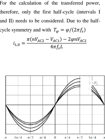
During steady-state operation, the voltages vAC1(t) and vAC2(t) and the inductor current repeat every half-cycle with reversed signs since the phase shift time Tϕ and the DC supply voltages V1 and V2 remain the same during the first and during the second half-cycle (time intervals I, II and III, IV in Fig. 17, respectively).
For the calculation of the transferred power, therefore, only the first half-cycle (intervals I and II) needs to be considered. Due to the half-cycle symmetry and with 𝑇𝜑= 𝜑/(2𝜋𝑓𝑠)
𝑖𝐿,0 =
𝜋(𝑛𝑉𝐴𝐶2− 𝑉𝐴𝐶1) − 2𝜑𝑛𝑉𝐴𝐶2
4𝜋𝑓𝑠𝐿
results for positive phase shift, 0 < φ < π, and a similar result is obtained for negative phase shift, −π < φ < 0. The transferred power results :
P =nVAC1VAC2φ(π−|φ|) 2π2fsL
for each value of the φ will be :
P > 0 denotes a power transfer from the HV to the LV port and
P < 0 denotes a power transfer from the LV to the HV port.
Fig. 17 Transformer voltages and inductor current for phase
shift modulation
Fig. 18 Transferred power vs the phase shift for the DAB
23 The achieved power transfer for the DAB converter is depicted in Fig. 18 and shows a maximum for a certain phase shift angle; the maximum power transfer is analytically evaluable by solving the following equation, ∂P/∂ϕ=0, that is :
|P𝑚𝑎𝑥| =nVAC18fVAC2
sL for φ = ±π/2
This circuit configuration, however, offers the alternative types of modulation that changing the duty cycles of vAC1(t) and vAC2(t), well as the current waveform, allow to reduce the RMS value of the current flowing in the transformer / inductor especially on the side at low voltage and at the same time reducing the switching losses.
Fig. 19 shows a typical trend of the duty cycle of vAC1(t) and vAC2(t) for which the RMS current of the inductor has the minimum value versus the
transferred power level.
Having regard to the modest values of the average power that the modulator should handle the DC/DC converter must necessarily operate in triangular current mode. Therefore the design choices of the DC / DC converter will be focused to determine the optimal modulation in the case where it operates in triangular current mode with V1 > nV2.
In the triangular current mode modulation (Fig. 20. a) the LV side full bridge solely switches at zero transformer current causing low switching losses but the HV side full bridge switches zero transformer once per half period causing high switching losses.
Fig. 20 a) Transformer voltages and inductor current for triangular current mode modulation
b) Modified triangular current mode modulation which enables HV side ZVS and LV side switching at zero transformer current.
a) b)
Fig. 19 Duty cycles D1 and D2, which minimize the
24
Therefore, to obtain the low total switching losses, the modulation scheme needs to be modified, such that the LV side full bridge continues to switch at zero current and the HV side full bridge is operated with ZVS. The required modification to the modulation scheme introduces circulating transformer currents (Fig. 20. b), needed to achieve ZVS on the HV side. With this modified triangular modulation scheme, the maximum achieved power is far below the maximum possible power of the DAB.
Based on the lossless electric DAB model, the required duty cycles and the required phase shift angle are determined with:
Typical efficiency values that can be obtained with this type of DC/DC converter are between 90% -95% and this is the greater since the ratio between the output voltage and the input voltage tends to the transformation ratio n.
The project of the aforementioned DC/DC converter and its controller is complex and requires a more detailed discussion is beyond the above mentioned study. On the other hand there are today commercially available subsystems capable of providing the requirements summarized in the following table and employing the technologies described in this paragraph.
6 Charging unit
In order to achieve a high repetition accuracy, the capacitor bank has to be charged to the desired voltage with a high accuracy between two pulses. This task is performed by a charging unit which must ensure that the voltage drop of the capacitor bank is contained within less than drop voltage specification. The stored energy in solid state modulators generally is much bigger than the pulse energy.
In fact, the size of the capacitors bank is a function of the percentage voltage drop and the peak voltage. The charging unit must therefore, at start-up storing the energy necessary to achieve of the peak pulse voltage. Conversely, between each pulse will be required to integrate the energy transferred to the load, which is a negligible fraction of the total stored energy .
The size of the capacitor bank can therefore be a technological limit not easy to be solved. In fact, with the increase of the capacitive value grow the parasitic effects, which worsen the dynamic behavior. The main parasitic effects are manifest in the form of ohmic losses and reactive effects, due to the presence of leakage inductances.
25 While, the first type of effect it worsens the voltage drop with the increase of the current supplied from the capacitor, the second type of effect, in the presence of variation of the current, can give rise to oscillatory phenomena that can generate hazardous overshoot for semiconductor devices used as switches.
One way to overcome this obstacle is to resort to the simultaneous use of: - Multicore transformer,
- Charging unit operating in interleaved mode.
The use of multicore transformer, in fact, allows to distribute of the energy, which overall must be accumulated by the sole bank of capacitors, in a number of capacitors equal to the number of cores from which the multicore transformer is constituted. Reduced size of the capacitors makes possible to use capacitors that have better dynamic performance.
Also, the total current required by the charging unit operating in interleaved mode will present a low ripple, it will result:
𝐼𝑟𝑖𝑝 ∝ 1 𝑁2
where N is the number of the charging unit. In this way the dynamic performance requests to the preceding stage are less stringent and therefore the output capacitor of the last stage, which must be of a size comparable to the sum of the output capacitors of the individual charging units, may present less performing physical characteristics.
Another requirement to the charging unit is to increase the voltage level in order to ensure the pulse generator the correct voltage level to be modulated and converted by the pulse transformer.
6.1 DC/DC boost converter
Based on the requirements of the charging unit, the most suitable circuit appears to be that of the DC/DC boost converter. Moreover, to ensure a conversion efficiency comparable or superior to that of the remaining subsystems, since the output converter will raise the input voltage, it is possible to make operate this stage in boundary conduction mode (BCM) in other words the switching of the switches is occur at zero voltage (ZeroVoltageSwitching). This circuit solution allows to consistently reduce the switching losses, to reduce the size of the converter itself and simplifies the voltage balancing between the switches in series. In fact, the advantages and disadvantages between this operative mode and the continuos conduction mode (CCM) are summarized in the Tab. 3.
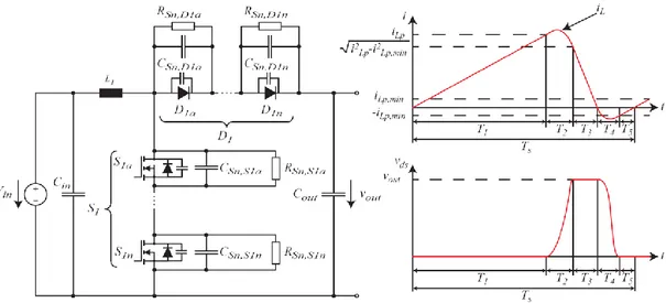
The boost converter is an electronic circuit device able to transfer energy at high level between the generator and the output load. This exchange of energy takes place through almost two reactive elements L1 and Cout. The different energy level of the output is controlled by the charge and discharge of inductor that is connected in series with the output capacitor.
In order to explain the operation mode of the circuit converter (Fig. 21 a) is needed to divide the time in four interval considering that the operation is cyclic (Fig. 21 b). During the interval T1 the switches are turned ON
26
and the input voltage Vin is applied to the inductor L1. Therefore the inductor current iL increases until the switches turn OFF. The inductor current reaches the level iLp
[A2] .
In the first part of the interval T2 the switches are turned OFF and the diodes are not conducting until the snubber capacitors does not start charging. In this case the inductor L1 and the snubber capacitors CS of the switches and diodes form a resonant circuit.
The inductor current iL at this point (interval T3) will tend to decrease as the capacitors in parallel to the diodes and the output capacity tend to charge.
[A2] ∆𝑖 𝐿𝑟𝑖𝑠𝑒=𝑉𝐿𝑖𝑛 1 𝑇1 , ∆𝑖𝐿𝑓𝑎𝑙𝑙= 𝑉𝑖𝑛−𝑣𝑜𝑢𝑡 𝐿1 𝑇3
Tab. 3 Advantages and disadvantages between CCM and BCM
Continuos Conduction Mode Boundary Conduction Mode Peak current: 1 ≤2 RMS current: 1 ≤ .57 AVG current: 1 ≤ .5 Size Magnetics: 1 0.4
Power losses switch on:
1 ≤ .25
Power losses switch off:
1 ≤ .16
Common Mode noise:
27 Obviously, while the maximum value of the positive voltage across the snubber capacitors will be limited by the conduction voltage of the diodes the voltage across the output capacitor will grow up to the value : 𝑣𝑜𝑢𝑡= 𝑣𝑖𝑛+ 𝑣𝐿= 𝑣𝑖𝑛+ 𝐿1𝑑𝑖𝐿 𝑑𝑡 = 𝑣𝑖𝑛+ 𝐿1 ∆𝑖𝐿𝑟𝑖𝑠𝑒 𝑇3 ≈ 𝑣𝑖𝑛(1 + 𝑇1 𝑇3)
Since the 𝑇3 interval can at most be less than or equal to 𝑇1, the inductor current iL at beginning of the interval 𝑇4 will be zero (Zero Voltage Switching Boundary condition) if it is verified this relation ∆𝑖𝐿𝑟𝑖𝑠𝑒 < ∆𝑖𝐿𝑓𝑎𝑙𝑙 that implies :
2 𝑉𝑖𝑛− 𝑣𝑜𝑢𝑡 < 0 Eq. 1
In the interval T4 again the inductor and the parasitic capacitors form a resonant circuit. During the time interval T4 the body diodes of the switches begin to conduct bringing quickly the switches in the conduction zone. In this way is concluded a whole controlled cycle of energy transfer.
The resonant transition during interval T4 can be modeled as a resonant circuit with an equivalent capacitance of
𝐶𝑒𝑞= 𝐶𝑆𝑤𝑖𝑡𝑐ℎ+ 𝐶𝐷𝑖𝑜𝑑𝑒 Eq. 2 The input capacitor is modeled as a voltage source. At the beginning of the resonant transition, Ceq is charged to the output voltage and the inductor current is zero. With these initial conditions and assuming a linear capacitance, the circuit oscillates around the input voltage with an amplitude of Fig. 21 a) Boost converter scheme, b) waveform of the inductor current and the mosfet drain-source voltage.
Fig. 22 Upper limit for Vin to achieve ZVS for different
28
𝑣𝑜𝑢𝑡− 𝑉𝑖𝑛 . In a real system, the assumption of a linear equivalent parasitic capacitance is not entirely valid.
The capacitances of the semiconductors show a strong voltage dependency. Because the capacitance increases significantly at lower voltages, more energy would be required to meet the ZVS condition.
However the influence of the non-linear capacitance of the semiconductors is reduced by the additional snubber capacitors. In Fig. 22 is shown the upper limit of the 𝑉𝑖𝑛 to achieve ZSV in function of the 𝑉𝑜𝑢𝑡 and the snubber capacitors Cs.
Inside the ZVS operating area, a minimum inductor current is required to transmit power to the output. The minimum current for linear capacitances is:
[A3]
where C is the equivalent capacitance during the resonant transition and L is the boost inductance. If the converter is operated below iLp,min no power is transmitted to the output.
6.1.1 Series Connection of Switches
Since the system is operated at an output voltage of 3 kV, a series connection of several MOSFETs and diodes is required. To assure a balanced blocking voltage across the series connected devices, a snubber network, consisting of a parallel of resistor and capacitor, are added as shown in Fig. 21 The resistor assures a static voltage balancing since the leakage current is in general not equal for all devices. The capacitors assure a balanced voltage across the switches during transients. These capacitors are required because the output capacitances are not equal and the MOSFETs do not switch at the same time instant due to jitter in the switching signals and component tolerances. The voltage difference of the blocking voltage after the turn off process can be described as follows:
where io denotes the current through the switches during the turn off process, T is the jitter between the turn off signals and C is the snubber capacitance for assumption equal at each blocking voltage.
6.1.2 Converter Control
The controller that modulates the turn-on time interval can operate in one of two ways: - by an on-time control,
- by a peak current control.
[A3]
So that we can transfer energy from the inductor to the capacitor is necessary that current flowing into the capacitor C. This current must be equal to: 𝑖𝐶 = 𝐶∆𝑉∆𝑡𝑜 where it is: ∆𝑉𝑜= 𝑣𝑜𝑢𝑡− 2𝑉𝑖𝑛.
The energy transferred to the capacitor will therefore equal to: ∆𝐸 =12𝑖𝐶𝑣𝑜𝑢𝑡∆𝑡 and it will have to match the
decrease of energy in the inductor equal to: ∆𝐸 =12𝐿 ∙ 𝑖𝐿𝑝,𝑚𝑖𝑛2. Therefore, by sharing the two equations and
29 Both methods are mathematically equivalent. The peak current control additionally provides an over-current protection and is independent of the exact turn-on time of the switch.
The disadvantage of this control strategy is that the source current of the MOSFETs has to be measured. The on-time control requires only a zero-crossing detection of the inductor current in order to determine when the on-time starts.
In order to achieve a high repetition accuracy, a closed loop control is required. The feedback controller for the on-time control differs from the peak current control. The optimal time instance to turn on the switch is always at the end of T4, regardless if ZVS is possible or not. This reduces the losses, since the conduction losses of the switch are lower than those of the internal body diode.
Since the converter is operated in BCM, the switching cycles are independent as the converter could stop operating at the end of each cycle. Hence, it is possible to use a cycle to cycle based feedback controller which calculates the required peak current iLp or the on-time Ton depending on the implemented converter control. Therefore the converter can be controlled by using an adaptive, time discrete controller. The change of the output voltage 𝑣𝑜𝑢𝑡,𝑛+1− 𝑣𝑜𝑢𝑡,𝑛 for a capacitive load within one switching cycle is:
[A4]
with:
The required peak switch current can be calculated by using previous reports with 𝑣𝑜𝑢𝑡,𝑛+1= 𝑣𝑜𝑢𝑡,𝑠𝑒𝑡 :
[A4]
It is possible to evaluate this relationship, starting from the following equations: 1 2𝐿 ∙ 𝑖𝐿𝑝 2=1 2𝐶 ∙ (𝑣𝑜𝑢𝑡,𝑛+1− 2 ∙ 𝑉𝑖𝑛) ∙ 𝑣𝑜𝑢𝑡,𝑛+1 1 2𝐿 ∙ 𝑖𝐿𝑝,𝑚𝑖𝑛 2=1 2𝐶 ∙ (𝑣𝑜𝑢𝑡,𝑛− 2 ∙ 𝑉𝑖𝑛) ∙ 𝑣𝑜𝑢𝑡,𝑛
subtracting both members of the two equations and rewriting everything according to the following amount: 𝑣𝑜𝑢𝑡,𝑛+1− 𝑉𝑖𝑛 it will arrive : 𝐿 𝐶∙ (𝑖𝐿𝑝2− 𝑖𝐿𝑝,𝑚𝑖𝑛2) + (𝑉𝑖𝑛− 𝑣𝑜𝑢𝑡,𝑛) 2 = (𝑣𝑜𝑢𝑡,𝑛− 𝑉𝑖𝑛) 2
30 with :
For an on-time control based controller, the on-time can be calculated with:
A schematic of the control hardware is shown in Fig. 24. The control hardware incorporates three measurement inputs: the converter input voltage, the output voltage and the switch current. The voltages are measured by using an RC voltage divider. The source current of the MOSFETs is measured with a shunt. The measured signals are fed via a pre-amplifier stage to the ADC inputs and the comparator input respectively.
The input and output voltage are sampled by an ADC which is connected to an FPGA. The feedback controller output is converted to an analog output signal by an DAC. This signal is then compared with the measured switch current in order to determine when the switches have to be turned off for a peak current controlled system.
The switch control implemented in the FPGA generates the switching signal depending on the operating conditions. Finally, the switching signal is converted into an optical signal which is transmitted to the converter. The design of the converter controller, implies to control the behavior of the charging unit at an impulsive change in load. In other words for the design of controllers it needs to dimension the parameters (parasitic resistance of the capacitor ESR) that influence the output dynamic impedance.
31 7 Pulse generator
In an pulse modulator, the electronic stage that is technologically more complex to be designed and implemented is the pulse generator. This stage can be decomposed into the following subsystems:
- commutation Switch, - Pre-magnetising circuit, - Pulse transformer, - possible L-C Bouncer,
interconnected according to the layout shown in Fig. 25.
Before proceeding with the detailed description of each subsystem it is necessary to contextualize the overall layout to the case under study. Therefore is necessary to briefly summarize the project parameters that constrain the design/implementation and these are:
the maximum peak voltage to the modulator output,
the maximum rise time, overshoot and drop voltage of the step response, the maximum energy transferred per pulse.
It will start by evaluating the effect of accumulated energy and transferring from the modulator, in fact the energy transferred to the load at each pulse is a small fraction of the energy that is needed to store to obtain the preset value of the flattop voltage.
This consideration therefore obliges the designer to evaluate all the circuit solutions that allow to accumulate large electrostatic energies and to release them small quickly (capacitors with low ESR, capacitors with a high density of storage energy).
The first solution, that can be used, is distribute the electrostatic energy to be storage with multiple charging units connected to the same bank of input capacitor. Additionally, using an interleaved mode control of
32
charging units during the period when the output voltage to the modulator is null, it is possible to assure a low distorted current demand at the previous stage.
The second solution, which integrates with the first one, is to convey the electrostatic energy, previously fractionated, to the load and simultaneously raising the value of the flattop voltage. To this purpose, the pulse transformer used to increase the output voltage is made by several ferromagnetic cores. In this way, using a single secondary winding that concatenates the magnetic flux of individual cores, it is possible to obtain a high output voltage without having to resort to a high number of secondary coils (reduced the output distributed capacity) and to ensure the required energy transfer.
Therefore in this way it is possible to use a further parameter in the design phase to observe the constraint on the output voltage at the flattop and the pulse rising time.
Precisely in this circumstance, the relationship of the transformation ratio, besides, depend on the turns ratio will also depend on the relationship between the concatenated magnetic flux. In fact, unlike a normal transformer where the concatenated primary flux is practically equal to the concatenated flux to the secondary, in a multicore transformer, the secondary flow may be higher than the primary flow or vice versa. Thus indicating with A1 the average area enclosed by the primary spirals and with A2 the mean area enclosed by the secondary spins will result :
𝑉2 𝑉1 = 𝑛𝑐𝑜𝑖𝑙,𝑙𝑒𝑔∙ 𝐴2 𝐴1 where it is : 𝑛𝑐𝑜𝑟𝑒 =𝐴𝐴2 1 𝑛𝑐𝑜𝑖𝑙,𝑙𝑒𝑔= 𝑁2 𝑁1
This solution by acting on the number ncore of the magnetic core allows to contain the number of turns of the secondary winding and improve the rise time that depends on the square of the latter.
Another resulting advantage is a reduction in magnetic and electrostatic energy accumulated between the primary and secondary winding with respect to the case where the secondary windings are connected in series.
In fact, in the example shown in Fig. 26, with the same total magnetic flux and in compliance with the safety distances[A5] between primary and secondary windings, it is possible to see the difference of dimensions (hatched areas) between a solution in which has a number of secondary windings connected in series equal to
[A5]
The safety distance dw,minbetween primary and secondary winding depends by the Epeak maximal tolerable peak electic field in oil (20kV/mm for short pulses of few microseconds), rr the inner radius of the cylinder (guard ring) and vs the secondary voltage, according to the following relationship:
33 the number of magnetic cores and that in which is present a solution with only two secondary windings each spanning all the magnetic cores.
In general, this transformer configuration is called the multicore-transformer [5].This type of transformer for its peculiarities must be made with primary windings at a reduced number of turns. In fact we shall see in the following paragraphs that with the increase of the number of cores decreases the magnetic flux density for the core, and then the number of primary winding turns.
Furthermore, in the case of medium-large energy transfers per pulse, to optimize the value of ampere-turn per core, it is preferred to use a solution with two switches per core (see Fig. 28) to halve the current handled by each switch and halve the energy managed by each Charging unit stage.
If the pulse duration is short (µs order), since that the pulse energy transfer is low, to reduce the flux leakage at the primary, a double primary winding connected in parallel is used. In fact, it must remember that, how much less is long the time rise of the magnetomotive force as much less the magnetic flux penetrates the center of the core (magnetic skin depth) and therefore the greater is the magnetic reluctance of the core. This effect involves the re-closing of the flow along the external lines at the magnetic core and thus a leakage inductance increase. Therefore, to counteract this increase of the leakage inductance and of the magnetizing current is used a redistribution of the magnetomotive force for each transformer leg.
In summary, the primary winding of the multicore-transformer is made with a few coils, ( ribbon type or conductive film type) wrapped around each leg of the magnetic core and connected in parallel at only one switch per core.
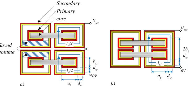
Fig. 26 Saved volume between the primary and secondary windings, resulting in a reduced leakage inductance
when using (b) the matrix transformer, instead of (a) a transformer series connection. U sec 0V l w/2 b k d w ak dw l w/2 a) U sec 0V 2bk dw ak dw lw’ b)
core
Primary
Secondary
Saved
volume
Fig. 27 Schematic of the solid-state modulator with two
cores, two primary windings arond each core, and secondary enclosing both cores.
34
The secondary winding in a similar fashion will consist of only two windings connected in parallel, opportunely isolated from the individual primary windings, arranged so as to embrace each half of the legs from which is composed the multicore-transformer.
In Fig. 28 is shown, by way of example, the construction of a multicore-transformer consisting of only two magnetic cores.
This solution allows, by comparison, a reduction of the:
overall volume,
number of winding turns, flux leakage,
electrostatic energy stored between primary and secondary windings.
In other words, this solution will reduce the leakage inductance 𝐿𝜎1, 𝐿𝜎2 and the distributed capacitance 𝐶𝑑, which depend on:
𝐿𝜎1∝ 𝑁12∙ 𝑉12 𝐿𝜎2∝ 𝑁22∙ 𝑉12 𝐶𝑑 ∝ (𝑁2
𝑁1)
2
∙ 𝑉12
where 𝑁1 , 𝑁2 are the winding turns and 𝑉12 is the volume between the windings.
Another problem, that occurs only in the HV pulse transformers due to the constraint on the interlaminar voltage is the necessary oversizing of the magnetic-core cross-section. In fact, if the pulse energy transferred from the transformer to the load is low, the dynamic of the flux swing is small and thus also the cross-section required.
However, for assigned magnetic tape with which the core is made, if the interlaminar voltage is higher than the maximum permissible voltage, the designer is forced to oversize the magnetic core, so as to increase the number of sheets per cross section[A6]. Whatever the solution used to feed the multicore-transformer, in order to reduce the
[A6]
To reduce the interlaminar voltage, it is possible:
- reduce the voltage on the primary windings by increasing the number of magnetic cores, - increase the interlaminar dielectric resistance,
- dividing the cross section of the core.
Fig. 28 Schematic of the solid-state modulator with two
cores, two primary windings around each core fed in parallel from a single switch per core, and secondary enclosing both cores
35 switching losses is important to synchronize opportunely the switches using to an active gate control.
In fact, a possible delay of the switch SM,2 respect at the SM,1, results in the creation of an induced current in the primary winding (green trace), which circulates in the freewheeling diode Df,2. When the SM,2 switch is in "on" state, the Df,2 diode will continue to be crossed by current, even though it is inversely polarized, due to the release time of the accumulated minority charges near the emptying region. In this case, to balance the current on the second primary winding, it is necessary to compensate the spilled current by the diode by increasing the current supplied by the switch. Therefore, this operating condition creates a stress for both the freewheeling diode that for the switch (see Fig. 29).
The active gate control will allow to monitor the voltage and the current in the switching phase, so as to schedule the gate signal of the switches and to avoid a hard commutation of the freewheeling diode and protecting the modulator from a potentially dangerous overcurrent to the load (arc current monitor).
In the paragraphs that follow describe in detail the technological solutions adopted for each of the subsystems shown in Fig. 25, focusing on the design criteria to be adopted in order to realize a pulse transformer to work with secondary voltages next to a million volts.
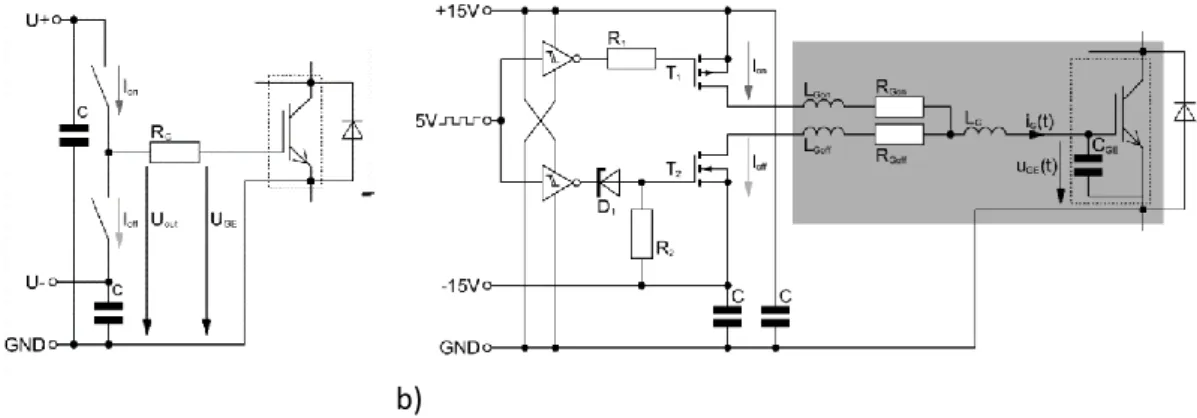
7.1 Switches and driver circuits in the pulse generator
The primary winding voltage modulation is obtained by semiconductor devices such as IGBTs (Insulated Gate Bipolar Transistor), which unlike the other semiconductor devices show a good compromise between the voltage/current switching and the maximum switching frequency. However, the IGBTs have advantages and disadvantages. The disadvantages of these devices are the lower blocking voltage and lower current rating compared with spark gaps. Therefore, multiple semiconductor switches have to be connected in series and/or in parallel. To reduce the number of required switches, they have to be operated at the highest current as possible.
The efficiency of a pulse generator, from the point view of the switching devices, depends on the conduction losses and the switching losses of the IGBT. While the first depend essentially on the constructive physical characteristics of the device, the latter depend on the driver circuit.
IGBT Conduction losses can be calculated using an IGBT approximation with a series connection of DC voltage source (vCE0) representing IGBT on-state zero-current emitter voltage and a collector-emitter on-state resistance (rC):
𝑣𝐶𝐸(𝑖𝐶) = 𝑣𝐶𝐸𝑂+ 𝑟𝐶∙ 𝑖𝐶
The same approximation can be used for the anti-parallel diode, giving:
𝑣𝐷0(𝑖𝐷) = 𝑣𝐷𝑂+ 𝑟𝐷0∙ 𝑖𝐷
These important parameters can be read directly from the IGBT Datasheet (cf. Fig. 30) and increasing these to a safety factor that is typically between 1.1. and 1.2 .