Alma Mater Studiorum · Universit`
a di Bologna
Scuola di Scienze
Dipartimento di Fisica e Astronomia Corso di Laurea Magistrale in Fisica
A Flexible Readout Board for HEP
Experiments
Relatore:
Prof. Alessandro Gabrielli
Correlatore:
Dott. Gabriele D’Amen
Presentata da:
Giuseppe Gebbia
Abstract
This thesis will present my contributions to the development of the “πLUP” board along with a general overview of its features and capabilities. The πLUP board is a general-purpose FPGA-based readout board for data acquisition systems under develop-ment by the University of Bologna and the Instituto Nazionale Fisica Nucleare (INFN) and intended for high energy physics experiments, where the sheer amount of data gen-erated by detectors often requires custom hardware solutions.
This board was initially proposed for the next upgrade of the ATLAS Pixel detector. In this context its purpose would be to interface the Front-End readout chip RD53A with the FELIX card and provide advanced testing features such as an emulator for the RD53A that will help the development of the other parts of the data acquisition chain. Nonetheless, since the early stages of development, the hardware has been designed to offer great flexibility so that the same hardware platform could be directly used in other applications. To this purpose an important feature of the board is the great extendibility offered by the presence of different interfaces, such as and 3 FMC connectors (two low density and one high density), a PCI Express x8 interface, gigabit ethernet and an integrated SFP connector.
The computing power of the πLUP is provided by of two FPGAs, a Zynq-7 SoC and a Kintex-7 produced by Xilinx, intended to be used in master-slave configuration. In this case the Zynq, with its dual-core ARM processor and the possibility to run an embedded linux distribution, would be used as main interface with the other functionalities in the board. The main objective of this thesis is the development of such software and firmware control infrastructure, starting from the firmware solutions for the inter-FPGA communication to the low-level software to control the system.
Sommario
In questa tesi saranno presentati i miei contributi allo sviluppo della scheda “πLUP” insieme ad una panoramica delle sue funzionalit`a e applicazioni. La πLUP`e una scheda di readout general-purpose basata su tecnologia FPGA in sviluppo da parte dell’Universit`a di Bologna e l’Istituto Nazionale di Fisica Nucleare (INFN). La scheda `e mirata ad applicazioni in sistemi di acquisizione dati per esperimenti di fisica delle alte energie, nei quali l’elevata quantit`a di dati generati dai sistemi di rilevazione richiede spesso l’utilizzo di soluzioni hardware su misura.
Inizialmente la πLUP `e stata proposta come soluzione per il prossimo upgrade del Pixel Detector dell’esperimento ATLAS. In tale sistema il suo utilizzo consisterebbe nell’interfacciare il chip di front-end RD53A con la scheda di readout FELIX, mettendo a disposizione funzionalit`a di testing, come ad esempio un emulatore per il RD53A, per facilitare lo sviluppo delle varie parti della catena di acquisizione dati. Nonostante questo, fin dalle prime fasi di sviluppo, l’hardware della scheda `e stato progettato per offrire grande flessibilit`a in maniera da poter adattare la stessa piattaforma a diverse applicazioni. A tal fine un importante caratteristica di questa scheda `e la presenza di diverse interfacce fisiche che contribuiscono all’estensibilit`a delle scheda, come ad esempio 3 connettori FMC (due a bassa densit`a ad uno ad alta densit`a), un connettore PCI Express ed un SFP+.
La πLUP `e dotata di due FPGA, un SoC Zynq-7 ed una Kintex-7 prodotte da Xi-linx, tipicamente utilizzate in una configurazione master-slave. In tale configurazione la Zynq, che include un processore ARM dual-core con la possibilit`a di supportare una distribuzione Linux completa, sarebbe l’interfaccia principale con le funzionalit`a presenti sulla scheda. Lo scopo principale di questa tesi `e lo sviluppo di tale struttura firmware e software.
Contents
1 Introduction 2
2 The ATLAS Experiment 5
2.1 Inner Detector . . . 6
2.2 Calorimetry and Muon Tracking . . . 8
2.3 Trigger System . . . 10
2.4 ATLAS Pixel Detector . . . 11
2.4.1 Future Upgrades . . . 14
3 The πLUP Platform 21 3.1 Hardware Overview . . . 21
3.2 Firmware Control Infrastructure . . . 27
3.2.1 Inter-FPGA communication . . . 28
3.2.2 AXI Register Block . . . 29
3.2.3 Interface with the Software . . . 31
4 Applications 34 4.1 Protocol Converter . . . 34 4.2 RD53A Emulator . . . 37 5 Conclusions 39 Appendices 40 A FPGA Architecture 41 B Transmission Protocols 46 B.1 The AXI Protocol . . . 46
B.2 Aurora 64b/66b . . . 48
B.3 GigaBit Transceiver (GBT) . . . 50
Chapter 1
Introduction
The πLUP board (pronounced “pile-up”, an acronym for PIxel detector Luminosity UP-grade board) is a readout card developed by the university of Bologna and the Instituto Nazionale Fisica Nucleare (INFN) section of Bologna for experiments in high energy physics. Most experiments in this sector involve huge data rates and/or very strict timing requirements from quite complex sensor systems; for example the entire ATLAS experiment, in its current state, generates a raw data-rate with an order of magnitude of 1 petabyte/s. In this context, the role of a readout card is interface with the front-end electronics (mixed-signals devices that read and digitalize the information from the sen-sors) and to process the incoming raw data, generally performing data formatting and monitoring, which may include some form of on-line analysis.
The πLUP was initially developed to be part of the upgrade for the DAQ of the ATLAS experiment pixel detector in view of the next Large Hadron Collider (LHC) luminosity upgrade, that will increase the luminosity to the maximum design value [1]. In high energy physics experiments the luminosity L is defined as the proportionality factor between the number of events N generated per unit of time and the cross section σ of the event:
dN
dt = L · σ (1.1)
This value characterize the ability of the machine to produce a certain scattering event, and so the luminosity upgrade aim to increase the number of collisions per unit of time. The next major upgrade of the LHC (during the period referred as Long Shutdown 2) plan to increase the luminosity by an order of magnitude to increase the probability of observing rare events (characterized by a small σ) at the various experiments present along the LHC circumference. As an obvious consequence, this implies an equally sizable increase of the already huge amount of data to be processed and stored, making it necessary, among the others, to replace several parts of the aging pixel detector DAQ system, currently based on the “ROD-BOC” system [2]. While the development of this board was justified by the need to replace said system, the πLUP aims to be a
general-purpose readout card, capable to adapt to different use cases and experiments. Additionally, the board comes equipped with a software and firmware infrastructure that will ease further developments in view of any possible future application by providing higher-level control over the functionalities implemented in the board and in particular in the FPGAs firmware.
A picture of the latest version to date is shown in fig.1.1, while a block schematic showing the main components present on the board in fig.3.1 in the next chapter. The board is based on two Xilinx FPGAs, a Zynq SoC and Kintex, used in a master-slave configuration. The Kintex acts as the “muscle” of the board, driving the higher speed interfaces and running most of the more complex firmware applications. The Zynq on the other side, with its integrated ARM CPU, acts as the main control interface to the board and so can be considered as the “master” of the system. In most applications studied the ARM processor runs an embedded Linux distribution. The choice to include a Zynq FPGA was mostly driven by such need to have a generic (hardware) CPU on the board and between the wide choice of ARM-based SoC an FPGA-based SoC was deemed to be the most interesting to met the flexibility and extendibility target set by the project; indeed the reconfigurability offered by such systems make it easier to repurpose and adapt the board to other uses by allowing to implement new features and fix flaws long after the hardware design is completed.
A variety of different I/O interfaces also adds to the versatility of this board; some of the most useful are the PCI Express connector and the SFP+. The PCIe connectivity is a standard choice for a read-out or DAQ card, since it is one of the most common
and sensible options to interface and transfer data with an host computer. The SFP+ connector offers a higher bandwidth alternative, possibly over optic fiber connection, to the two gigabit ethernet ports, one of which is connected to the Zynq processor and is one of the main “access points” to communicate with the system. Additionally three FPGA Mezzanine Connectors (FMC), a Low-Pin Count (LPC) and a High-Pin Count connected to the Kintex and another LPC connected to the Zynq, leave wide room to interface the board with other devices.
The following discussion in divided in three chapters: The first will describe in broad terms the data acquisition system of the ATLAS experiment and its recent developments. In the second, after a quick overview of the πLUP hardware, the firmware and software infrastructure implemented on the board will be described. Finally in the last chapter some specific applications developed will be presented, and in particular the protocol converter between the RD53A and the FELIX card, as well as the emulator for the former.
Chapter 2
The ATLAS Experiment
The ATLAS (A Toroidal LHC ApparatuS) experiment is one of the major experiments at the Large Hadron Collider (LHC)[3]. The detector, shown in fig.2.1, is a massive general-purpose particle detector designed to detect the variety of particle produced by collisions between high energy (up to 14 TeV) protons at its core. At the current state of the LHC, after the run-2 upgrade, at interaction point bunches of ∼ 1011 protons
from the two beams cross with a peak rate of 40 MHz, generating a total of 6 · 108 proton-proton collisions per unit of time (only ∼ 20 collisions per bunch crossing) [4].
As expected from the broad definition of the problem, the detector is composed of
several “sub-detectors” specialized in reconstructing specific observables from different particles. The entire system has a cylindrical geometry, with detectors placed in both surfaces; barrel-shaped detectors with orientation parallel to the direction of the beam are referred as “barrel” detectors while the ones placed on the base of the cylinder, and so with orientation incident to the beam, “end-caps” detectors.
The collision point between the two beams, right at the centre of the cylinder, is taken as origin of the coordinate system, with the x axis pointing to the centre of the LHC ring and the y axis in a direction normal to the circle (and consequently, z along the same direction of the beam). Generally the coordinate system is expressed in polar variables, with φ being the azimuthal angle and θ the polar angle. The trajectory angle of a particle produced by the collision respective to the beam axis is expressed by the pseudorapidity η = − ln (tan (θ/2)).
2.1
Inner Detector
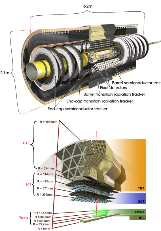
As suggested by its name the inner detector (ID), schematized in fig.2.2, is the innermost layer of ATLAS, and therefore the closest to the beam (and the collision point). Data from this detector is mainly used to perform particle tracking, and so its purpose is to detect the passage of charged particles, reconstructing spatial and temporal informations about the event. Using these informations is also possible to measure the energy of the particle from the trajectory of the particle; to this purpose the ID is submerged in a strong magnetic field (∼ 2 T) that curves the trajectory of charged particles, allowing to measure their momentum from the curvature once the particle is identified.
The ID is in its turn composed by three sub-detectors: the pixel detector, the semi-conductor tracker (SCT) and the transition radiation tracker (TRT). Each offering a different trade-off in terms of granularity, precision and area covered.
Pixel Detector The pixel detector is composed of four barrel-shaped matrices of sil-icon pixels plus 3 end-caps rings (with pixel modules orthogonal to the direction of the beam rather than parallel), offering the highest level of granularity (i.e. spatial resolution) near the beam where the (spatial) density of events is the higher. Its data acquisition system is of main interest to this work, and a more detailed description of this detector and its DAQ system will be provided later in this chapter.
Semiconductor Tracker The successive 4 layers are part of the SCT, also including 9-layers end-caps; this is also a silicon-based detector, but each module of the “pixel” matrix is composed by a series of elongated microstrips (with a width of 80µm and length 12 cm) rather than squared pixels. While this detector offers a lower precision compared to the pixel detector, the SCT covers a larger area. Together, the pixel detector and the SCT cover the pseudorapidity area |η| < 2.5.
Figure 2.2: Cut-away of the inner detector (top) and placements and distance of the three barrel sub-detectors from the beam (bottom).
Transition Radiation Tracker Last, the TRT is composed by 4 mm diameter straws with orientation parallel to the beam in the barrel part and perpendicular at the end-caps. Each tube is filled with a gas mixture of Xe(70%)CO2(27%)O2(3%) (recently the Xenon
was replaced with Argon for cost reasons) and the straw shell is kept at a negative high potential with respect to an anode wire running along the centre of the straw. A charged particle crossing this structure generates a ionization in the gas that can be measured as a current signal between anode and cathode. Additionally the space between the straws is filled with polymer fibers to generate transition radiation that can be absorbed by Xe atoms. This two event can be distinguished by the front-end electronics by the strength of the current signal.
The TRT doesn’t offer a spatial resolution competitive with the other two detectors, but its lower cost respect a pixel-based detector (and also inherent physical structure) allows to build a more extensive apparatus, offering more precise momentum estimation of the particle by measuring more points in a larger range along a track.
2.2
Calorimetry and Muon Tracking
The role of the calorimeters is to measure the energy of a crossing particle. The general design of a calorimeter employs a series of layers with a high probability of interaction with the particles of interest interleaved with detectors able to measure the occurrence of an event and/or the amount left by it. A calorimeter must be then designed to fully contain the particle shower generated by one particle interacting with the detector, which is the factor that determine the (often quite extensive) physical extension of the detector. While all the calorimeter systems offer some information about the position of the event with various level of granularity, the precision is definitely not comparable with the inner detector and so the information from those detectors is not directly intended for track reconstruction. The calorimeters are mainly used for particle identification and so are also crucial for the triggering system.
The different calorimeter systems are designed to interact with different particles: the innermost Liquid Argon (LAr) electromagnetic calorimeter is divided, as shown in fig.2.3, in a barrel element covering the pseudorapidity region |η| < 1.475 and three end-caps: the EM end-cap (EMEC), plus the hadronic end-cap (HEC) and forward (FCal) calorimeters, covering the range 1.375 < |η| < 3.2. The LAr EM calorimeters are designed to absorb electrons and photons, and are composed by a series of alternating layers of absorber elements (typically a metal such as lead or copper) and layers filled of liquid argon that ionize when an high-energy particle crosses it. The HEC overlaps in the same pseudorapidity area of the EMEC to detect hadronic particles non absorbed by the latter. Similarly, particle not contained by the LAr barrel calorimeter are absorbed by the tile calorimeter, which detection system is based on layers of scintillating tiles (i.e. photonic signals) rather than electric signal in a ionized medium.
Figure 2.3: Cut-away of the calorimeters system [3].
Muon System The last and most external (and also large) detector is the muon spectrometer, covering the range |η| < 2.7. In a similar manner to the inner detector, the muon spectrometer employs strong magnets to deflect the trajectory of muons (which pass across the other detectors mostly undisturbed due their low cross-section) to a series of detecting chambers to estimate their momentum. There are various types of detector chambers: the precision tracking chambers composed by the Monitored Drift Tubes (MDT) covering most of the pseudorapidity range and the Cathode Strip Chambers (CSC) which offer higher granularity in the 2 < |η| < 2.7 pseudorapidity region; the trigger chambers covering the |η| < 2.4 range and divided in Resistive Plate Chambers (RPC) in the barrel section and Thin Gap Chambers (TGC) in the end caps.
As suggested by the name, the role of the precision tracking chambers is to track the trajectory of the muons to get precise estimations of their momenta. The detection method is again based on ionization of a gas mixture caused by the inelastic collision with the charged muons. The difference between MDT and CSC is related to the higher density of tracks in the pseudorapidity range covered by the latter, which made it neces-sary to employ a more complex detector system with better multi-tracks discrimination capabilities.
The precision chambers are complemented by the trigger chambers, which are based on similar principles for the detection of muons but are designed to provide a fast response to use in the trigger system (which as will be explained later puts very strict limits to
the timing in order to generate a response).
2.3
Trigger System
To deal with the enormous data rate coming from the various detectors, the ATLAS experiment uses a multi-stage trigger and data acquisition system (TDAQ) which exploits a subset of the available detector to select interesting events to be acquired and stored. The main components of the TDAQ system are schematized in fig.2.4. The Level 1 Trigger is hardware-based (FPGA or ASIC) and uses part of the information from the muon trigger chambers and the calorimeters to detect possible events of interest, such as the generation of particles with high transverse momentum. A Central Trigger Processor (CTP) then uses this informations to take a decision in under 2.5µs (the time between bunch crossings) and in case triggers the detector read-out drivers (ROD) to read the
Level-1 Le ve l-1 A cc ep t Level-1 Muon Endcap
sector logic sector logicBarrel
Level-1 Calo CP (e,γ,τ) CMX JEP (jet, E) CMX Central Trigger MUCTPI L1Topo CTP CTPCORE CTPOUT Preprocessor nMCM Detector Read-Out ROD FE ROD FE ROD FE ... DataFlow
Read-Out System (ROS)
Data Collection Network
Data Storage Muon detectors
Calorimeter detectors
High Level Trigger (HLT) Processors O(28k) RoI Event Data Fast TracKer (FTK) TileCal Accept P ixe l/S CT Tier-0
Figure 2.4: Block diagram of the TDAQ system of the ATLAS experiment showing the two main trigger blocks (Level-1 and HLT) and their interacion with the readout and acquisition system [4].
buffer pipelines from the front-end electronics (FE) holding the data from the detectors (including the inner detector). Since both the signals in the calorimeters and the muons flight-time in the detector are longer than the bunch crossing interval, another crucial role of the L1 trigger is to track the number and timing of the bunches crossing and attach to the trigger signal informations related to the exact bunch that generated the event. The L1 trigger also builds a Region of Interest (RoI) map of the event, that will used by the rest of the system for a more accurate analysis of the data selected in this fist triggering stage. After the L1 trigger filtering the date rate is reduced to about 75 kHz. To the L1 trigger follows the software-based High Level Trigger (HLT, in turn com-posed by the Level-2 Trigger and the Event Builder), which runs on “conventional” CPUs and reduces the rate to ∼200 Hz performing a deeper analysis around the RoI detected by the L1 trigger using the full data from the detectors. This includes tracking informa-tion from the inner detector so the L2 trigger performs an approximate reconstrucinforma-tion of the event in the RoI. Finally the data selected by the HLT is stored in the Tier 0 data center for off-line analysis.
An additional Fast TracKer (FTK) [5] is under development and intend to use infor-mations from the inner detector for an intermediary stage between the L1 trigger and the HLT. This system will be based on FPGA and custom ASIC chips and will imple-ment fast parallel tracking algorithms, based on associative memories, for track fitting. This will provide the HLT with precise track informations even at higher event rates not manageable with conventional CPUs.
2.4
ATLAS Pixel Detector
As previously introduced, the ATLAS pixel detector is composed by 4 barrel-shaped matrices of pixels plus end-caps organized as shown in fig.2.5: the B Layer, the Layer 1 and 2 [3], and after the Run-2 upgrade by the Insertable Barrel Layer (IBL)[6, 7]. The three original pixel layers are composed by a matrix of 63.4 mm × 24.4 mm sensor modules each containing 47232 pixels of nominal size of 50µm × 400 µm, while in the IBL layer the pixel size is reduced to 50µm × 250 µm to obtain a higher resolution. The modules are mounted on staves with pitch of ∼ 20 degrees for the L1–2 and BL, and ∼ 14 degrees for IBL as shown in figure. The modules along a stave are also slightly titled in the z axis (along the stave length) in the direction of the interaction point to increase the geometric acceptance. Together, the four layers have in total 1680 modules. Other than the pixel sensors itself every module includes the front-end chips to read and digitalize the information from the sensor, and a Module Chip Controller (MCC) distributing timing, trigger and calibration signals and also generating events for the Read-Out electronics. The IBL modules present a number of differences from the ones in the other three layers: they are based on the newer FE-I4 front-end chip (succeeding the FE-I3 adopted in the other layers) which communicates with the readout electronics
Figure 2.5: 3D view of the Pixel detector (top), barrel and stave structure of the IBL (bottom). The scheme on the bottom also shows the pixel technology used along a IBL stave [6].
directly without the need of a MCC. In the IBL, other than the already mentioned pixel size, the pixels are not all identical; the 3 older layer use a planar silicon technology, while the IBL combine in the same stave planar pixels with pixels based on a 3D technology, as shown in the bottom part of fig.2.5. In 3D pixels the electrodes are realized by etching of vertical columns crossing the device, reducing the charge drift distance since the distance between electrodes is no longer fixed by the wafer thickness and so can be arbitrary. This leads to improvements in response times, bias voltage requirements and potentially smaller probability of trapping by impurities (which might mitigate the effects caused by radiation damage).
The front-end chips, schematized in fig.2.6, are directly bonded to the pixel sensors and so is exposed to great doses of radiation as well. The FE-I3 was fabricated with 250 nm CMOS technology with various radiation hardening techniques. Good part of the chip area is occupied by the pixel read-out cells; each cell is composed by two analogue parts (based on a buffer and amplifier stage, and a programmable amplitude comparator) reading data from two pixels, and a digital part which transfer the address of the hit and the Time over Threshold (ToT) to the hit buffers at the periphery of the chip. Those buffers must be deep enough to hold the data until the L1 trigger accepts or discards an
event (up to 2.5µs of data).
The much bigger FE-I4 [8] used in the IBL, based on 130 nm CMOS technology, has been designed to deal with the increased radiation exposition and higher data rates caused by the shorter distance from the collision point, especially in view of future luminosity upgrades that would overflow the FE-I3 hit buffers. As can be seen from fig.2.6 the new chip abandons the centralized memory/logic approach in favour to a distributed memory architecture; read-out cells are consequently much bigger, also reading 4 pixels rather than 2, and including on the digital part per-pixel Hit Processors and FIFO data buffers, and per-cell trigger logic as well. The Hit Processor calculates the hit Time over Threshold and append a time-stamp, this information is stored in the pixel dedicated buffer to be then transmitted to the End of Chip Logic only in presence of a trigger. The use of Hamming coding for both intra-chip and external communication increase the device yield. From the End Chip Logic the data is streamed out with 8b/10b encoding at a rate of 160 Mb/s via E-Link serial protocol communicating directly with the readout electronics.
Figure 2.6: Layout of the FE-I3 chip [3] (left) and the FE-I4 [8] (right).
The Pixel Detector ReadOut Driver electronics is based on the IBL ROD-BOC sys-tem [2] schematized in fig.2.7; this is composed by a series of paired FPGA-based cards, the ReadOut Driver (ROD) and the Back Of Crate (BOC), connected via VME bus.
The BOC board reads and configures the front-end modules (16 per board in the case of the IBL layer, more for the other layers where every modules requires a smaller band-width), communicating with the front-end over the optical e-links. The data received is sent via VME bus to the ROD board in the same crate which performs data formatting, which consist mainly in data packaging attaching an header with metadata such as trig-ger informations. Formatted data is sent back to the BOC which in turn forwards it to the ATLAS data acquisition system via S-Link protocol. The ROD additionally acts as interface to configure the font end modules and build the calibration histograms, that are sent via ethernet to a server farm for further analysis.
Figure 2.7: Block diagram of the ROD-BOC readout drivers [2].
2.4.1
Future Upgrades
During the planned shutdown from the start of 2019 to the start of 2021 (the “Long Shutdown 2” preceding the Run-3 operations) the LHC and its experiment will receive extensive upgrades to reach the collider design operating energy and luminosity. This section will introduce two new components of interest for this discussion that will have an important role in the future of the ATLAS TDAQ. The first one is the new FELIX Readout Driver [9] system, that will gradually replace the entire ROD and readout system starting from the run 3, with full introduction expected for the run 4. The other relevant project is the RD53A font-end module [10], which is mainly intended to deal with the increased luminosities of the High Luminosity upgrade (run 4), and aims to study and develop font-end architectures for future pixel detectors not limited to the ATLAS experiment.
RD53A The RD53A chip is a demonstrator prototype for the next generation of pixel front-end chips designed to deal with the increased datarate and radiation from the LHC High Luminosity upgrade. It is based on 65 nm CMOS technology and adopts (and extends) the distributed memory approach of the FE-I4 to efficiently cope with higher datarates.
The layout of the chip is schematized in fig.2.8. A peculiar characteristic is the “analog islands” design, where squared block of analog electronics (the “islands”), containing 4 analog front-end each reading a different pixel, are embedded in a “sea” of synthesized digital logic composing the digital part of the pixel read-out logic. This includes buffering, ToT computation, triggering and read-out. The analog islands are further organized in groups of 16, composing a “pixel core” (which reads a matrix of 8 × 8 pixels), as schematized in fig.2.9. Pixel cores are stacked in columns, with each element relaying the information from the previous core to the next. This hierarchical organization is necessary to include “regional” buffers to manage the high amount of data and avoid saturation of the bandwidth along a column.
While all elements in a single column are identical, for evaluation purposes the chip area is divided in three regions each adopting a completely different design for the analog front-end that will be characterized against the different intended uses of this chip. In any case, as usual, the information from the analog front-end consist in a logical signal
Figure 2.9: Block diagram of a RD53A digital core [10], several cores are stacked in rows to obtain a pixel matrix.
indicating that the analog signal from the pixel is in that particular instant higher than a certain programmable threshold (from this then follows the computation of the ToT). The analog front-ends also include an injection circuit driven from the digital logic necessary to generate test pulses for calibration.
The digital pixel region logic also comes in two variants: the Distributed Buffer Architecture (DBA) and Central Buffer Architecture (CBA). The main difference is that DBA stores the ToT values in dedicated per-pixel buffers, while the CBA uses a common buffer for each core with the advantage of performing zero suppression of ToT values but requiring the storage of a 16-bit hit-map (if null ToT values are removed, it is necessary to record which of the 16 pixels in the core generated the hit associated with each stored ToT value). The memory efficiency trade-off of the two architectures generally depends on the pixel logic region size, density of events and bit precision for the ToT counters. In the RD53A for the DBA the region size chosen is 8 rather than 16, and both DBA and CBA use 4-bit ToT.
The data from the digital core columns is read from the Digital Chip Bottom (DCB) at the periphery of the chip. This serializes the data according to the Aurora 64b/66b protocol generating an output over up to 4 lines with strict alignment (see section B.2) at 1.28 Gbps each. The DCB includes the control logic to decode external commands, received from a E-LINK [11] interface at 160 Mbps, and is also connected to the Analog Chip Bottom (ACB) containing, as suggested by the name, all the required analog cir-cuitry (for example configure the analog front-ends bias or ToT threshold, the PLL for the E-link clock recovery and the Aurora transceiver, etc. . . ).
In its Aurora implementation the RD53A defines 5 custom command blocks, referred as “register blocks”; the output stream format consist of N data frames (with the asso-ciated separator block at the end of each data frame) interleaved with a single register
block, as shown in fig.2.10. The value of N is user-programmable, allowing to control the fraction of bandwidth dedicated for data. Fig.2.10 also explains the format of both data and register frames: A data frame can be composed by an Aurora data block (a) formatted with two 32-bit blocks of data (containing, as shown, hit data with address of the event and ToT data, or an even header with trigger trigger informations), a sep-arator command block with 0 or 4 octets valid indicating the end of a data frame (b and c, with c also used to signal idle), or an Aurora specific status/idle command block (d). Finally, register frames (e) are composed by a single custom command block (with possible type codes “zz” documented in the manual) containing a 4-bit status code and the address/value of two registers. The registers transmitted are either requested by an external command or selected automatically, the two cases are distinguished with a different command block code.
Figure 2.10: Schematics of RD53A output format [10].
FELIX The Front End LInk eXchange (FELIX) is the new front-end Read-out Driver developed mainly for the ATLAS TDAQ, but also of interest for other projects. Even inside the ATLAS experiment the FELIX platform is not intended only for the pixel detector read-out, but is planned, by the time of the Run 4, to interface with the en-tire Front-End and Trigger system, inclusive of all detectors mentioned in the previous section. One of the main goals of the FELIX project is to reduce the complexity and maintenance burden of the ATLAS TDAQ system, right now largely based on custom hardware specific to each (sub)-detector, by introducing commercial off-the-shelf hard-ware as soon as possible in the data acquisition chain, as schematized in fig.2.11. The board itself, based on a Virtex-7 FPGA and featuring a 16 lines Gen 3 PCI-Express
Figure 2.11: ATLAS DAQ with the (partial) introduction of the FELIX system [9].
connector, will be mounted in a commercial server setup. For this reason the FELIX card is often described as a “detector-agnostic data router”, relaying data from the front-end to a commodity switched network composed by conventional server implementing any further data processing in software (referred as SW ROD). The introduction of a switched network based on commercial standards instead of point-to-point links with custom hardware is also another advantage, making the system more flexible and in principle easier to extend.
Fig.2.12 illustrate the Felix system and the structure of the firmware in the FPGA. The connection with the front-end is over optical lines using either the radiation hardened Gigabit Transceiver Protocol (GBT, see section B.3) or the Felix “FULL mode” protocol (section B.4), with the latter offering twice as much bandwidth (9.6 Gbps). The FULL mode protocol is currently only implemented for downlink from the front-ends, since for command transmission the bandwidth offered by the GBT is generally sufficient. Currently there are a number of Felix platform in use, the version used in this work is the “Mini-FELIX”, a revision made available for initial development and offering 4 SFP+ connectors that can be used for an equal number of GBT/FULL mode links. The latest final prototype, the BNL-711, offers 48 bidirectional optical links via MiniPOD transceivers although the PCI-express link is not able to manage all of them running at
their full bandwidth. The board also distributes TTC signals to the font-end, and so the firmware includes a dedicated TTC processor.
As said, data is exchanged between the FPGA and the host server (running a linux distribution) via PCI-Express x16 bus, accessing the host machine system memory with a custom-made DMA engine (Wupper Core [12]) offering a simple FIFO-based stream interface. The DMA engine transfers the received data to a large circular buffer on the system memory. This buffer is allocated on a contiguous area of physical memory to simplify the DMA operations and maximize performances. The PCIe x16 link is actually split in two x8 channels due a limitation of the PCIe End Point IP core provided by Xilinx. The two channels work independently and are connected to the same PCIe x16 connector by means of a dedicated on-board switch IC (Broadcom PEX8732); consequently on the host system a Felix card will be detected as two different devices, but both are managed by the same driver and control software instance.
The Felix server is connected to a switched network through optical connections based on commercial networking hardware and industry standards such as ethernet and
EDR infiniband with link speeds up to 100 Gbps. Being a “data router”, the Felix system itself doesn’t perform any form of manipulation on the data from the front-ends, apart from packetization and in general anything necessary to propagate data on the switched network. Any operation on the data (such as formatting, fragment building, or histogramming) is performed in software by a farm of server individually connected to the network (the SW ROD shown in fig.2.11). The Felix network stack is implemented by the NetIO library, which, in short, serve the received data with a publish–subscribe model to the SW ROD in the network and also route commands from the DAQ system to the front-end.
This approach allows to use commercial hardware and flexible software solutions for any detector-specific application, with custom-made general-purpose hardware (i.e. adaptable to any detector) relegated to generic data routing purposes.
Chapter 3
The πLUP Platform
3.1
Hardware Overview
The first hardware design of the πLUP was based on two prototype boards, the ZC702 and the KC705, produced by Xilinx which also distributes the schematics, so most com-ponents present on those boards are also present on the πLUP. The idea was to put together in the same board a “conventional” FPGA chip, providing the main computing power for the particular applications intended for this board, and a SoC including a CPU to ease control and monitoring operations, which are in general implemented in software. For this purpose a Zynq SoC includes a fairly performant ARM-based embedded with an FPGA, offering all the advantages of a full (but in this case smaller) secondary FPGA, which adds to the flexibility of the board. A block diagram showing the main hardware features of the πLUP is presented in fig.3.1.
Consequently the processing power of the board is delivered by two 7-series Xil-inx FPGAs, a Zynq-XC7Z020 integrating a dual-core ARM Cortex-A9 processor and a Kintex-XC7K325T, used in a master-slave configuration and connected by a bus com-posed by 21 differential lines plus 5 single-ended lines. A full characterization of this bus has not been performed yet, but some stress-tests employing the 21 differential lines using the LVDS (Low Voltage Differential Signaling) I/O standard resulted in a reliable source-synchronous transmission up to 200 MHz DDR (Double Data Rate), resulting in a total bandwidth of 8.4 Gbps, without the need of performing a deskewing calibration on the single transmission lines. This is widely sufficient for the intended use of this bus since, as said, the Zynq will access the firmware components implemented in the Kintex mostly for configuration and monitoring purposes. In the future, would some application require an higher bandwidth between the two FPGAs, it should be possible to gain a higher bandwidth employing the SERDES present in the FPGA I/O blocks. Since not all of the 21 FPGA pin are connected to the same I/O bank, for a source-synchronous transmission this would require splitting the bus in smaller units, or using a self-clocking
Ether net x2 HPC LPC LPC 1GB DDR3 Zynq Kintex SFP+ PCIe x8 sma SO -DIMM DDR3 UAR T x2 USB JTAG
Figure 3.1: Logical components on the πLUP.
protocol that doesn’t need a dedicated clock line such as the Aurora protocol. A brief overview of the FPGA I/O resources is presented in Appendix A, while the system used for the communication between the two FPGA is discussed later in this chapter.
In terminology used by Xilinx for their SoC devices, the FPGA-side of the chip is called Programmable Logic (PL) and the “static” ARM-based system Processing system (PS). A block diagram describing the structure of a Zynq SoC, with particular attention to the PS feature, is shown in fig.3.2. Apart from the APU (Application Processor Unit), featuring two ARM CPUs with 256 KB of on-chip SRAM (OCM), the PS also includes controllers for a variety of interfaces, including a DDR3 memory controller. The main channels of communication between the PS and the PL are the General-Purpose and High-Performances AXI ports (the AXI protocol is briefly described in appendix section B.1). In particular the latter can give direct access to both the OCM and DDR controller, allowing high speed DMA transactions between PS and PL (12.8 Gbps per channel). As said, since the main role of the ARM will be control and monitoring without the need for exchange of large quantities of data, most application studied employ only the GP ports. There are 2 GP AXI ports available with 1 GB of address space each (the complete address map of the PS can be found in ref.[14] ch.4). The system also feature 16 PS-PL interrupts lines that can be used hook the logic implemented in the FPGA fabric directly to the APU Global Interrupt Controller (GIC).
Figure 3.2: Block diagram of the Zynq Processing System, from [13].
I/O Interfaces Since the main purpose of the πLUP is front-end readout, the board present a number of high speed interfaces, many of which are connected to the Kintex FPGA. The Kintex features 16 integrated multi-gigabit transceivers (MGT) divided in 4 different FPGA I/O banks and capable of speeds up to 12 Gbps. Their use is distributed between the various interfaces present in the board as shown in table 3.1. Half of the available transceiver are employed for the 8-line Gen 2 PCI Express connector, which is capable of a (raw) datarate of 4.0 GB/s and is the main interface to exchange data with an host machine. A high speed external interface is offered by the 10 Gb/s SFP+ connector. For instance, in an application such as the protocol converter for the FELIX that will be discussed in the chapter 4, this interface is used to communicate with the FELIX board when only one optical link is required. Another transceiver is connected to a differential SMA connector pair, than can be used for a high speed card-to-card communication over coaxial copper cable. This solution, while noticeably cheaper than an optical link, is extremely limited in range especially at higher speeds.
I/O Bank MGT I/O iface 115 0 PCIe lane 7 1 PCIe lane 6 2 PCIe lane 5 3 PCIe lane 4 116 0 PCIe lane 3 1 PCIe lane 2 2 PCIe lane 1 3 PCIe lane 0 117 0 SMA 1 Gb Ethernet 2 SFP+ 3 FMC LPC 118 0 FMC HPC 0 1 FMC HPC 1 2 FMC HPC 2 3 FMC HPC 3
Table 3.1: Usage of FPGA MGT.
The two gigabit ethernet interfaces, one connected to the Kintex and the other to Zynq, are present mainly to offer a control interface to the board. To this end the Zynq ethernet has particular importance since it will be the main “user access window” to the board; this port is driven by the dedicated ethernet controller in the Zynq PS, on which is quite simple to implement a full network stack and utility services. On the other way, the ethernet on the Kintex side will be most likely removed in a future revision, redirecting its transceiver to alternative applications (such as an additional SFP+ connector).
As it is common on FPGA platform, the πLUP features some FMC connectors: one VITA 57.1 LPC FMC connectors for each PFGA chip plus another HPC FMC for the Kintex, the latter also connected to 4 MGTs. FMC connectors leverage the reprogrammable nature of FPGAs to define a standard daughter-card connection which allow to extend the board with a substantial variety of commercial or custom devices. For this reason it was considered a sensible design choice to dedicate a good part of the FPGAs I/O resources to FPC connectors.
Fig.3.3 shows the Bit Error Rate (BER) eye diagrams for some of the transceivers. The diagrams were acquired at a speed of 10 Gb/s transmitting a pseudo-random binary sequence in a loopback configuration using the Integrated BER test (IBERT) IP core provided by Xilinx [15]. The eye diagrams for the transceivers connected to the HPC FMC were acquired connecting an FMC board providing 4 SFP+ connectors (FM-S14
FMC), again in a loopback connection. The IBERT test was ran until a BER of 10−14 was reached, which satisfy the requirements requested by CERN for data acquisition hardware. Apart from the SMA test, the eye open area is also satisfactory.
Figure 3.3: Eye diagrams for the Kintex MGTs, in left-right top-bottom order: the 4 FMC, SFP+ and SMA.
The I/O capabilities are complemented by other low-speed interfaces present on the board such as the two USB-UART (Universal asynchronous receiver-transmitter) bridges, again one for the Zynq and the other for the Kintex, and various GPIO headers not shown in fig.3.1. Both are mainly intended for debugging and development purposes. The unused I/O interfaces offered by the Zynq PS (schematized in fig.3.2), are also connected to GPIO headers, so it is possible to experiment with them in case some interest should arise.
Memory Devices 1 GB of DDR3 RAM, required for the operations of the ARM processor, is soldered directly on the board and controlled by the DDR controller in the Processing System, which offer exactly 1 GB of address space for the external memory. The Kintex is connected to a DDR3 SO-DIMM slot, with the maximum amount of RAM supported mostly limited by the FPGA firmware. The maximum speed of the memory bus is currently limited to 400 MHz, most likely due some timing violation related to the
traces length on the PCB. Future revisions of the board will aim to improve this value up to 800 MHz through a better design of the physical memory bus. This frequency is the maximum supported frequency by the memory controller PHY in the particular Kintex model chosen for the πLUP.
On-board non-volatile memory for storage is provided by 3 flash chips: a 512 Mb PC28F00AP30TFA NOR chip and a 128 Mb N25Q128 QSPI chip, both connected to the Kintex, and another N25Q128 connected to the Zynq. All three memories are used to store the firmware for the FPGA, but while the Kintex only need the programming bitstream, the flash connected to the Zynq will also have to hold the Linux kernel image and filesystem including any software developed. The 128 Mb (= 16 MB) offered by the N25Q128 flash chip, while being the biggest supported on a single QSPI chip by the Zynq integrated flash controller [14], resulted to be barely sufficient for the current use but generally an excessive limitation, especially considering the capabilities offered by the Zynq: as shown in the diagram in fig.3.2, the Zynq PS includes two SD memory controllers, but in the current board revision the pins associated with both controllers are connected to an header. Given the advantage of having a large easily writable memory on-board, especially during software development, as a temporary solution it was decided to produce a simple expansion card adding a SD socket to connect to said header; since the logic level of the SD controller is at 1.8 V but the SD cards communicate with 3.3 V, this card also includes a level-shifter IC specific for SD cards. Future revisions of the board will most likely include this simple circuit in the main board.
Other Components Apart for a few fixed crystal oscillators required by various com-ponents (such as two 200 MHz oscillators for the two FPGA system clock, the reference clock for the gigabit ethernet PHY, etc. . . ), the boards includes two Si570 programmable clock oscillators (again, one for the Zynq and another for the Kintex) and a Si5326 PLL, both programmable by I2C. The Si5326 feature two differential inputs and outputs, in
the πLUP one input and one output is directly connected to the FPGA pins and the other pair to a paired of SMA connectors couple.
Any component connected to the I2C bus is connected to the FPGA through a bus
multiplexer (PCA9548) to avoid collision between peripherals with the same hard-coded bus address; while the I2C components present on the board (the clock sources just described and a few EEPROM chips) have all different addresses, the I2C bus is also
connected to the FMC connector (as per VITA specification), which might be used con-nect daughter cards including components with conflicting I2C addresses. An important detail is that there are two separate I2C bus on the board, one controlled by the Zynq and
the other by the Kintex. For this reason it was necessary to implement a I2C controller
in the Kintex firmware, that can be nonetheless controlled by the Zynq PS thanks to the setup presented in the next section.
3.2
Firmware Control Infrastructure
This section describes the base frame of the firmware structure and in particular the implementation of the various control channels part of the master-slave structure of the two FPGAs. A block diagram that summarize the main components of this structure is shown in fig.3.4. As already said the ARM processor in the Zynq, running a Linux distribution, accesses the PL through the general purpose AXI ports shown in fig.3.2. This AXI bus is then transparently bridged to the Kintex using the AXI Chip2Chip IP core offered by Xilinx [16], allowing the ARM to access the peripherals present in the Kintex as if they where implemented directly in the Zynq PL. Any peripheral not offering an AXI interface can be controlled using a block of control registers addressable by AXI (as so directly addressable from the ARM). The various I2C-programmable devices are
controlled using another IP core, the “AXI IIC Bus Interface”, again provided by Xilinx. The main external access to this system is the ethernet connectivity on the Zynq; the use of a Linux distribution gives all the advantages that come with a full embedded operating system, offering to the developer a simple environment to control the system and develop software. It also makes it possible to easily offer network services such as an SSH server with also a webserver offering diagnostic informations and possibly more planned. Linux Chip2Chip master Chip2Chip slave 20 LVDS lines AXI SMARTCONNECT AXI register block AXI SMARTCONNECT AXI Periph. Custom Logic Ether net UAR T AXI I2C MUX Si570 Si5326
3.2.1
Inter-FPGA communication
The communication between the two FPGA is established with the Chip2Chip (C2C) IP core, which as just said transparently extend the AXI bus (plus an optional AXI-lite bus) from the master to the slave device. A block diagram describing the structure of this core is shown in fig.3.5. This core can be customized to fit a number of applications with different availability of I/O resources and required datarate for the inter-chip trans-mission. For the πLUP the main limitation is the number of available pins: consequently in the setup used the AXI interface has a data width of 32-bits and the channel multi-plexer is set to the highest multiplexing ratio available leading to a total occupation of 20 differential lines of the bus between the Zynq and the Kintex (9 data lines plus clock for each direction). The optional AXI-Lite interface is disabled since it would require more pins. The number of pins required also depend on the PHY type selected and clock settings, in this case the native “selectIO” interface with a rate of 200 MHz in DDR mode is used. In general the PHY can be clocked independently from the rest of the design to increase the throughput. Those settings give the smallest pin usage possible when using the SelectIO interface, the alternative would be to use the Aurora PHY interface which offer a way smaller use of pins (from 1 to 6 lines with a 128-bits AXI bus) but also requires a separate IP core managing the Aurora protocol and also a SERDES or even a MGT transceiver for every transmission line, depending on the desired transmission speed.
Figure 3.5: Diagram of the Chip2Chip IP core, extracted from [16].
The core also offers 4 dedicated interrupt channels per direction (master to slave and slave to master) that are given higher priority by the channel multiplexer over AXI data. In Zynq all slave-to-master interrupts are connected to the global interrupt controller (GIC) in the PS (see fig.3.2), which offer 16 interrupt channels. Only edge-triggered interrupts seems to be supported by the C2C core. In the case where more than 4 interrupts signals are required there are three possible solutions: First, the most common solution would be to share the same interrupt line between multiple peripheral, if supported by both the involved cores and drivers; this requires the peripheral to have
some internal register to store the interrupt state, so when the CPU receive an interrupt the drivers associated with the same line can check which peripheral was the one to actually generate the signal. If the design requires separate interrupts then it is possible to use the single-ended lines of the KZ bus (currently only one of the 5 lines available is occupied by a master to slave reset signal) as dedicated interrupt lines. Finally, an AXI Interrupt Controller IP core is offered by Xilinx, which allows to send interrupt to the Zynq via AXI bus and in this case would be connected to the C2C slave AXI interface. The C2C doesn’t require any special management during its operation; once out of reset, the system automatically start a calibration procedure, that also involves the deskewing of the single data lines employing the programmable delays present in the output block of the FPGA (see appendix A), and then is immediately ready to use. As shown in figure, the C2C feature only a AXI slave port on the master side and a AXI master port on the slave side, so the bridge is in a certain sense unidirectional (as only AXI master peripheral on the Zynq can initiate a read or write transaction with slave peripherals on the Kintex).
3.2.2
AXI Register Block
The structure of the AXI register block, schematized in fig.3.6, is quite simple. It is composed of two sequential arrays of 32-bit registers: “CTRL” registers that are read/writable from AXI and output their content to some logic, and “STATUS” regis-ters that are only readable from AXI and their content is updated at every clock cycle from some external signal.
To access the register the simpler AXI-Lite protocol is used, and the AXI address of a transaction is directly mapped to the address of a particular register. The behaviour of this core is similar to a simple memory, so the AXI transaction must be aligned to the 4 bytes boundaries. To select a particular 32-bit register the 3 least significant bits of the AXI address are discarded by the core to pass from the “bit-addressing” scheme
AXI4
LITE
32 bit wordST
A
TUS
CTRL
AXI ADDR 0x0 0x100 0x4of the AXI interface to the “byte-addressing” scheme of this core. In a write transaction it is possible to decide which bytes of the 32 bit words are actually written by means of the STROBE signal defined in the AXI specification.
In the application described in the next chapter, a single AXI register block is used to control any custom peripheral implemented in the Kintex. In general, while it would be the most preferable solution, not all peripheral use the same clock for their control interface, so different register ranges in this core will have to interface with different clock domains. Just sampling the asynchronous signal (i.e. registering its value in a flip flop (FF)) will most likely lead to metastability issues (the signal get sampled during its transition to another logic value violating the hold time of the receiving FF and making its output unstable). For a single signal the simplest solution is the double-FF register, shown in fig3.7: The asynchronous signal from clock domain 1 is sampled by a FF clocked with the destination domain clock, its output is possibly metastable so it is sampled again with another FF after 1 clock cycle. This assumes that the metastability stabilize after 1 clock cycle, otherwise it is possible to add others FF to the chain. Typically the Mean Time Between Failures (MTBF) of each stage is taken as [17]:
MTBFt=
et/τ
Twfcfd
(3.1)
where fcis the clock of the receiving domain, fdis the data toggling frequency and τ and
Tw system-specific constant that may depend on the operating conditions. In the Vivado
toolchain, the registers part of the synchronizer should be marked with the ASYNC REG constraint, so that the tool will try to place them as close as possible (possibly in the same CLB) to minimize the routing logic between them (and also skip the timing analysis on the path in question).
q
CLK1
CLK2
Figure 3.7: Double-FF signal synchronizer.
The FF-based synchronizer is not appropriate for multi-bit signals (or data buses in general), since a small timing difference between the various lines may cause corruption of one or more bits. If the data to be transmitted comes from a monotonic counter, then it may be possible to use a Grey counter, where the worst error would be a 1-bit delay of the counter. Otherwise for normal data an handshaking state machine is needed: in the source clock domain the data to be transmitted is frozen and a “data valid” signal
is generated. This is received by the destination clock domain which reads the data and generate an acknowledge signal. Finally the acknowledge signal is synchronized in the source domain so that it can move on the next value. The main disadvantage of this method is that the control signals exchange introduce a relatively high latency and so it is not feasible when the source domain need to transmit a new value too frequently. In this case a dual-clock FIFO is generally used (typically based on a dual-ported RAM and using Grey counters to move the value of the write and read pointers from one clock domain to the other).
Since the control registers will be read and written from software, which commands being sent occasionally compared to the clock of the design, the increased latency is not an issue in this case. Consequently this design for the πLUP employs simple three-stage FF synchronizer for single-bit signals and an handshaking FSM for multi-bit signals.
CLK2 Destination FSM Source FSM CLK1 data_valid ack DATA
Figure 3.8: Handshake-based data bus synchronizer.
3.2.3
Interface with the Software
The embedded Linux distribution is generated with the Xilinx Petalinux toolchain, which automatizes most of the steps required to build and deploy a linux image on the Zynq platform while also offering a fair level of customization.
The boot procedure is roughly schematized in fig.3.9, and proceed as follows [14]: the first code executed by the CPU once out of reset is stored in the bootROM implemented in the PS hardware and, being a ROM, not writable. All the other components are generated by the user (possibly with petalinux) and loaded via JTAG or saved on a memory in the board, the Zynq can boot from either the QSPI flash or an SD card. The main role of the BootROM is to determine the boot mode (set by a jumpers block on the board) and load the First Stage Boot Loader (FSBL). This, in turn, initialize the PS (sets its internal registers, initialize the DDR controller, etc. . . ), load the FPGA
bitstream and handoff the execution to the second stage bootloader, for which U-Boot is a very common choice for embedded systems. Only the FSBL along with U-Boot really need to be stored in some on-board memory: U-Boot features basic networking capabilities and is able to load the linux image from a remote server using the Trivial File Transfer Protocol (TFTP). When this is a viable option, the limitation given by a lack of an SD socket on the πLUP (mentioned in the previous section) is largely relieved.
BootROM FSBL U-BOOT LINUX
Stage 0 Stage 1 Stage 2
Figure 3.9: Zynq boot stages in order of execution.
The linux system prepared for this board features full networking support with an SSH server enabled by default, and additionally a number of drivers and utilities to control the peripheral in the FPGA are also included. Most AXI IP cores provided by Xilinx also ships with a driver, often part of the official kernel source tree. The kernel also includes drivers for the I2C multiplexer, which is managed transparently and just shows to the system the 8 multiplexed buses accessible from user space from the respective character device, and the Si570 clock generator, as part of the Common Clock Framework (CCF). It is possible to set the clock rate of the Si570 from user space thanks to a custom-made “userclk” kernel module that behaves in the CCF context as clock “consumer” and exposes a debugfs entry accepting an integer value for the new rate desired. The Si5326 PLL on the other end is programmed from a user space tool, which, given the input clock rate and two numerical values for a multiplication and
Kernel space usrclk
debug fs PLLFitter
(Si5326) Si570 AXI IIC UIO
User space /dev/uio
AXI Register
Block BUSI2C
division factors, calculates the optimal values of the required parameters and write them in the PLL register accessing directly the correct I2C multiplexed bus.
To implement user space drivers for peripherals controlled through the AXI register block, the best choice is most likely the Linux Userspace I/O (UIO) driver. This offers a simple way to develop drivers, with even the ability to manage interrupts, directly in user space. The UIO driver simply expose the memory space associated with a certain peripheral thought a character device (usually /dev/uiox) that can be simply mapped in the virtual memory space of an user space process driving the peripheral. This is in practice quite similar to accessing the system physical memory directly (through /dev/mem), but is much safer and “clean” and, as just said, it also offers a way to handle interrupts.
Chapter 4
Applications
This chapter describes the most relevant applications of the πLUP board developed to this date. The first one is a protocol converter to interface the Felix card with the RD53A front-end chip; as described in subsection 2.4.1, the data output of the RD53A uses the Aurora protocol while the Felix card can only transmit via the GBT or FULL mode protocols. The development of a protocol converter is then justified as a means to offer a solution to this incompatibility, and so offer a way to interface the two system during at least the testing phase of the system.
The other major application is an emulator for the RD53A chip entirely described in VHDL/Verilog and implemented in the FPGA logic. A front-end emulator is often useful in the development and testing of a data acquisition system, since it allows to run tests of the system even when the real chip is not available or lack the ability to generate simulated or real data in a convenient manner.
4.1
Protocol Converter
To interface the Felix card with the RD53A front-end chip, the πLUP will have to offer the electrical connectivity to interface with both components and then implement a firmware to convert the data from the RD53A, received via the Aurora 64b/66b, to the FULL mode protocol supported for the Felix downlink. Fig.4.1 shows a block diagram of the setups proposed for this application, with also the main components part of the πLUP firmware.
For testing and development the RD53A will be mounted on a custom PCB containing a single chip, referred as Single Chip Card (SCC) [18]. The digital input and output of the chip are both connected to a Display Port (DP) connector. As described in subsection 2.4.1 the RD53A can use up to 4 Aurora lines for the data output, occupying 4 differential lines of the DP link, and a single differential line for the e-link input. The DP connections on the πLUP can be provided with a FMC card, with two adapters already
πLUP
FELIX
RD53A
SCC
DP FMC DP e-link AuroraGBT_FPGA ConverterProtocol TTC
Encoder
SFP / FMC SFP
GBT
FULL mode
Figure 4.1: Block diagram of the protocol converter interfacing the Felix, connected via SFP+ optical links, with the SCC RD53A, employing a single DP connector for both e-link and 4 Aurora lines. The figure also shows the main firmware bocks implemented in the Kintex on the πLUP.
developed for the SCC [18]: an HPC single-chip card, used to connect a single SCC and offering additional connectivity for other interfaces present on the SCC intended for debugging and testing, and a LPC version multi-chip card, offering 4 mini-DP connectors and able to interface with 4 different SCC. Since each Aurora line transmits at a rate of 1.28 Gbps, the link doesn’t require the use of a MGT and can be driven using the SERDES integrated in the FPGA output logic. It should therefore be possible to interface the πLUP with 4 SCC using the LPC FMC, reaching a total downstream data rate of 20.48 Gbps.
When interfacing with a single SCC the connection with the Felix card can be estab-lished over a single optical fiber pair using the on-board SFP+ connector on the πLUP, which is well capable of sustaining the 9.6 Gbps data rate required by the FULL mode (and so the 4.8 Gbps GBT link in other direction). Otherwise, it is possible to use all the 4 optical links offered by the Mini-Felix card using another FMC card adding 4 SFP+ connectors (such as the commercial FM-S14 card), by employing the 4 MGT of the Kintex connected to the HPC FMC connector. The resulting 38.4 Gbps bandwidth would definitely be sufficient to read the 4 SCC that is possible to connect to πLUP.
Kintex FPGA. The GBT-FPGA is an open implementation of the GBT protocol written in VHDL and supporting various families of FPGA, with sources available on the GBT project website [11]. Commands received from the GBT are sent to the TTC Encoder block, which encodes them in the protocol expected by the RD53A (documented in ref. [10]) and send them over the serial e-link connection. For convenience the TTC Encoder can also generate trigger signals by itself at a configurable frequency, feature that reduces furtherly the hardware required for a test setup to use during development. As suggested by the fact that only one DP line is dedicated to the e-link, the RD53A chip expects commands and clock to be encoded in the same link. For this reason the GBT core must also recover the DAQ clock from the GBT data stream, which is then distributed to any component the need to be synchronous with the TTC clock.
A diagram showing the clock distribution in the πLUP is presented in fig.4.2; the 120 MHz reference clock for the MGT transceiver bank (SMA MGT REFCLK) used for the GBT receiver (GT TX) is generated from the Si570 chip and sent (via SMA connector) to the CPLL. The GT RX recovers the TTC clock encoded in the GBT data steam (RECCLK) which is then sent to a FPGA internal PLL (RECCLK MMCM) for use by other firmware blocks than need to be synchronous with the ATLAS clock and also to the external Si5320 PLL. The PLL is used to clean and multiply the recovered clock by a factor 2 to generate the 240 MHz clock required for the QPLL driving the FULL
Figure 4.2: Clock distribution in the Kintex, the GT* TX and GT* RX are the transceivers for the FULL mode and GBT respectively.
mode transceiver (GT RX). Given the limited maximum speed offered by the CPLL (as explained in Appendix A), the use of the QPLL for the FULL Mode link is required even when the transmission is over a single optical line.
Returning to fig.4.1, in the downlink direction the four Aurora lines from the RD53A are merged in a single FULL mode stream by the Protocol Converter. The output format of the RD53A has been described in subsection 2.4.1; the transmission over the 4 Aurora lines follows the strict alignment (see section B.2) and the data sent is parallelized over the 4 links according the their enumeration. The Protocol Converter decodes the Aurora stream and serializes the data received in a FIFO buffer, also attaching an header to describe the packet type (for example, to distinguish a RD53A register frame from a data frame). As mentioned in the previous chapter about synchronization methods, the buffer is a dual-clock FIFO and is needed for the high-throughput clock domain crossing between the Aurora and FULL mode driving logic. The buffer is then read from a finite state machine controlling and feeding data to the FULL mode implementation core according to the header attached to the data.
4.2
RD53A Emulator
To ease the development of DAQ system it can be convenient to develop an emulator for the RD53A chip. The emulator was implemented directly in the protocol converter firmware, as shown in fig.4.3, but can also be easily implemented standalone in any
πLUP
FELIX
GBT_FPGA ConverterProtocolTTC Encoder SFP / FMC SFP GBT FULL mode RD53A EMULATOR
FPGA board with sufficient resources.
The emulator is able to decode the commands from the Felix card and generate a coherent response according to the RD53A documentation. Currently some configuration parameters are fixed, such as the number of Aurora lines to use (fixed to 4), while anything related to the configuration of the analog part of the chip is simply recorded but doesn’t change the state of the system (i.e. the behaviour of the digital logic doesn’t change if the configuration of the ToT threshold or pixel bias voltage is altered since the analog part of the chip is not simulated and the data in generated arbitrarily). In presence of a trigger the emulator generates a dynamically configurable number of hits containing random data for the ToT value and row/column address of the event, but a valid trigger and event header (the RD53A output format is schematized in fig.2.10). The particular mechanism used for the random generator is not of particular importance since its only purpose is to produce data avoiding repetition of the same specific pattern, so the quality of the randomness is not an important parameter. For reference, the generator is a pseudo-random number generator based on a Linear Feedback Shift Register (LFSR) using some of the informations from the trigger for the initial seed.
Chapter 5
Conclusions
This thesis presented a general overview of the design efforts to produce a simple and extendible high-speed readout board. While most part of the discussion concerned its use in the ATLAS experiment, as described in the second chapter a number of design choices taken aimed at the realization of a board adaptable to different applications. In the same chapter a generic control interface, allowing simple communication between software and firmware, was presented. Such structure can be considered the basic “template” of a generic project employing the πLUP (i.e. a new application can directly reuse most of the work done with minimal changes), and was one the main points of this thesis.
The final chapter described the main applications developed for the ATLAS experi-ment, demonstrating how the features offered by the πLUP can be successfully used in one of the major HEP experiments; the protocol converter allows to interface the FELIX read-out board with the RD53A front-end chip, and the RD53A emulator is an useful tools for the development and test of the DAQ system.
Future works aim at both the improvement of current platform, with a number of hardware optimizations, and at the development of other applications. The current main target is the developments of a demonstrator capable of performing the readout and configuration of the RD53A SCC via PCI-express connectivity. Successive versions of the board will also adopt more powerful FPGA chips from the Xilinx higher line of products. This is of particular importance to extends the capability of the πLUP: other than the obvious advantages provided by a faster and larger FPGA logic, extra features such as more integrated MGT allows the upgrade the board I/O features with, for example, a Gen 3 16-lines PCI-express connector.
Appendix A
FPGA Architecture
Compared to the fist examples of this technology, modern Field-Programmable Gate Arrays (FPGA) are more “heterogeneous” systems consisting of different components specialized for different applications, often including dedicated digital components such as high-speed transceivers, entire CPUs (as in the case of the Xilinx Zynq platform), or even analog and mixed-signals systems. The major logic components typically found on
![Figure 2.1: Cut-away view of ATLAS showing the placements of its detectors [3].](https://thumb-eu.123doks.com/thumbv2/123dokorg/7410244.98307/8.892.144.744.680.1025/figure-cut-away-view-atlas-showing-placements-detectors.webp)
![Figure 2.3: Cut-away of the calorimeters system [3].](https://thumb-eu.123doks.com/thumbv2/123dokorg/7410244.98307/12.892.165.728.208.558/figure-cut-away-of-the-calorimeters-system.webp)
![Figure 2.4: Block diagram of the TDAQ system of the ATLAS experiment showing the two main trigger blocks (Level-1 and HLT) and their interacion with the readout and acquisition system [4].](https://thumb-eu.123doks.com/thumbv2/123dokorg/7410244.98307/13.892.176.714.535.968/figure-diagram-experiment-showing-trigger-interacion-readout-acquisition.webp)
![Figure 2.6: Layout of the FE-I3 chip [3] (left) and the FE-I4 [8] (right).](https://thumb-eu.123doks.com/thumbv2/123dokorg/7410244.98307/16.892.143.752.538.953/figure-layout-fe-i-chip-left-fe-right.webp)
![Figure 2.7: Block diagram of the ROD-BOC readout drivers [2].](https://thumb-eu.123doks.com/thumbv2/123dokorg/7410244.98307/17.892.106.794.408.698/figure-block-diagram-rod-boc-readout-drivers.webp)
![Figure 2.8: Layout of the RD53A [10]](https://thumb-eu.123doks.com/thumbv2/123dokorg/7410244.98307/18.892.181.724.639.1017/figure-layout-of-the-rd-a.webp)
![Figure 2.9: Block diagram of a RD53A digital core [10], several cores are stacked in rows to obtain a pixel matrix.](https://thumb-eu.123doks.com/thumbv2/123dokorg/7410244.98307/19.892.209.684.198.422/figure-block-diagram-digital-cores-stacked-obtain-matrix.webp)
![Figure 2.10: Schematics of RD53A output format [10].](https://thumb-eu.123doks.com/thumbv2/123dokorg/7410244.98307/20.892.134.755.479.758/figure-schematics-of-rd-a-output-format.webp)
