Engineering PhD School “Leonardo da Vinci”
PhD Course in
“Applied Electromagnetism in Electrical and Biomedical Engineering,
Electronics, Smart Sensors, Nano-Technologies”
PhD Thesis
Design and characterization of antennas
for wireless communications systems
ING/INF-02
Tutors:
Prof. Ing. Paolo NEPA ____________________________
Prof. Ing. Giuliano MANARA _______________________
Author
Ing. Roberto CASO
________________
2012
C
ONTEST
Contest ... 1
Journal Publications ... 5
Conference Publications ... 6
Introduction ... 9
1 Dual-Polarized Slot-Coupled Patch Antenna Excited by a Square Ring Slot ... 13
1.1 Introduction ... 13
1.2 A Square Ring Slot Feeding Technique ... 14
1.2.1 Introduction... 14
1.2.2 Antenna Design ... 16
1.2.3 Numerical and Experimental Results ... 20
1.2.4 Conclusions... 25
1.3 A wideband slot-coupled stacked-patch array for wireless communications ... 27
1.3.1 Introduction... 27
1.3.2 Antenna Design ... 29
1.3.3 Numerical and Experimental Results ... 31
1.3.4 Conclusions... 36
1.4 A Circularly Polarized 2x2 Array ... 37
1.4.1 Introduction... 37
1.4.2 Antenna Design and Experimental Results ... 38
2 Dual-Band PIFA for Wireless Communications Systems...45
2.1 Introduction ... 45
2.2 Compact Dual-Band PIFA for DVB-T and WLAN Applications ... 47
2.2.1 Introduction ... 47
2.2.2 Antenna Design and Experimental Results ... 48
2.2.3 Conclusions ... 57
2.3 Dual-Band L-Shape PIFA for Display-Equipped Devices ... 58
2.3.1 Introduction ... 58
2.3.2 Antenna Design and Experimental Results ... 59
2.3.3 Conclusions ... 63
3 Wideband Spiral Antennas...65
3.1 Introduction ... 65
3.2 Numerical Analysis of a Wideband Thick Archimedean Spiral Antenna ... 66
3.2.1 Introduction ... 66
3.2.2 Antenna Design ... 67
3.2.3 Dielectric Loading Miniaturization ... 72
3.2.4 Conclusions ... 76
4 Integration of Slot Antennas in Commercial Photovoltaic Panels for Stand-Alone Communication Systems ... 77
4.1 Introduction ... 77
4.2 Slot Antenna Design ... 80
4.2.1 Miniaturization effect due to the cover glass layer ... 83
4.2.2 Numerical analysis of the effect of the PV cells located nearby the slot . 86 4.2.3 A metallic reflector to get an unidirectional radiation pattern: its effect on the antenna input impedance ... 88
4.3 Experimental Results ... 91
4.3.1 Measurements results for the TSSA prototype ... 91
4.3.2 Measurements results for the SSA prototype ... 96
4.4 Conclusions ... 97
5 Design and Performance of an Integrated Antenna for a 433MHz Car Park Monitoring System ... 99
5.1 Introduction ... 99
5.2 Antenna design and performance ... 101
5.3 Conclusions ... 104
Conclusions ... 105
J
OURNAL
P
UBLICATIONS
1. R. Caso, A. D’Alessandro, A. Michel, P. Nepa, and G. Manara, “Integration of Slot Antennas in Commercial Photovoltaic Panels for Stand-Alone Communication Systems,” submitted to IEEE Transactions on Antennas and
Propagation, 2012.
2. R. Caso. A. D’Alessandro, A.A. Serra, and P. Nepa, “Dual-Band L-Shape PIFA for Display-Equipped Devices,” submitted to Electronic Letters, 2012. 3. A. Guraliuc, R. Caso, P. Nepa, and J. L. Volakis, “Numerical Analysis of a
Wideband Thick Archimedian Spiral Antenna,” to appear on IEEE Antenna
and Wireless Propagation Letters, 2012
4. R. Caso, A. D’Alessandro, A.A Serra, P. Nepa, and G. Manara, “Compact integrated dual-band G-PIFAs for DVB-T and WLAN applications,” to appear on IEEE Transactions on Antennas and Propagation, 2012
5. R. Caso, A. D’Alessandro, A.A Serra, P. Nepa, and G. Manara, “An Integrated Dual-Band PIFA for DVB-T and WIMAX Applications,” IEEE Antenna and
Wireless Propagation Letters, vol. 10, pp. 1027-1030, 2011.
6. R. Caso, A.A. Serra, A. Buffi, M.R. Pino, P. Nepa, and G. Manara, “Dual-Polarized Slot-Coupled Patch Antenna Excited by a Square Ring Slot,” IET
Microwaves, Antennas & Propagation, vol. 5, pp. 605-610, 2011.
7. R. Caso, A.A. Serra, M.R. Pino, P. Nepa, and G. Manara, “A Wideband Slot-Coupled Stacked-Patch Array for Wireless Communications,” IEEE Antenna
and Wireless Propagation Letters, vol.9, pp. 986-989186, 2010.
8. A. Buffi, R. Caso, M.R. Pino, P. Nepa, and G. Manara, “Single-feed circularly polarised aperture-coupled square ring slot microstrip antenna,” Electronics
Letters, vol. 46, pp.268-269, 2010.
9. A. Buffi, R. Caso, G. Manara, P. Nepa, and A.A. Serra, “Ring-slot coupled microstrip patch antennas,” Atti della fondazione Giorgio Ronchi, 2010. 10. R. Caso, A. Buffi, M.R. Pino, P. Nepa, and G. Manara, “A novel dual-feed
slot-coupling feeding technique for circularly polarized patch arrays,” IEEE
C
ONFERENCE
P
UBLICATIONS
11. R. Caso, A. Michel, P. Nepa, G. Manara, and R. Massini, “Design and
Performance of an Integrated Antenna for a 433MHz Car Park Monitoring System,” IEEE AP-S International Symposium, Chicago, Illinois, USA, 2012.
12. A. Michel, R. Caso, P. Nepa, L. Tavanti, L. Gazzarrini, and R. Garroppo, “Design and Performance Analysis of a Slot Antenna Integrated in a Photovoltaic Panel,” IEEE AP-S International Symposium, Chicago, Illinois, USA, 2012.
13. A.A. Serra, R. Caso, A. Buffi, A. Guraliuc, A. Michel, A. D’Alessandro, and P. Nepa “Research Activity on Antenna Design for Wireless Communication Networks at the University of Pisa,” IEEE AP-S International Symposium, Chicago, Illinois, USA, 2012.
14. R. Caso, A. D’Alessandro, A.A Serra, P. Nepa, and G. Manara, “Dual-band integrated G-PIFA antenna for DVB-T and WLAN applications,” IEEE AP-S
International Symposium, Spokane, Washington, USA, 2011.
15. R. Caso, A. D’Alessandro, A.A Serra, P. Nepa, and G. Manara, “Wideband integrated H-PIFA antenna for DVB-T and WIMAX applications,” IEEE AP-S
International Symposium, Spokane, Washington, USA, 2011.
16. R. Caso, A. Buffi, and A.A. Serra, “Ring slot coupled microstrip patch antennas,” RiNEm Riunione Nazionale di Elettromagnetismo, Benevento, Italy, 2010.
17. A. Buffi, R. Caso, M.R. Pino, and P. Nepa, “AR Bandwidth Enhancement for Single-Feed Circularly Polarized Square Ring Slot Patch Antenna,” EMTS
International Symposium on Electromagnetic Theory, Berlin, Germany, 2010.
18. A. Buffi, R. Caso, M.R. Pino, P. Nepa, and G. Manara, “Circularly Polarized Square Ring Slot Patch Antennas,” IEEE AP-S International Symposium, Toronto, Ontario, 2010.
19. R. Caso, A.A. Serra, M.R. Pino, P. Nepa, and G. Manara, “A wideband linear array of slot coupled stacked-patches,” IEEE AP-S International Symposium, Toronto, Ontario, 2010.
20. R. Caso, A. Buffi, M.R. Pino, P. Nepa, and G. Manara, “An annular-slot coupling feeding technique for dual-feed circularly polarized patch arrays,”
IEEE AP-S International Symposium, Toronto, Ontario, 2010.
21. A. Buffi, R. Caso, M.R. Pino, P. Nepa, and G. Manara, “A novel slot-coupling feeding technique for circularly polarized patch antennas,” IWAT International
22. A. Buffi, R. Caso, G. Manara, P. Nepa, and A.A. Serra, “Dual-polarization slot-coupled patch antennas: state-of-art and a novel configuration,” Giornata
di studio sulla caratterizzazione di antenne, Salerno, Italy, 2009.
23. R. Caso, A.A. Serra, P. Nepa, G. Manara, and M.R. Pino, “A square ring slot feeding technique for dual-polarized patch antennas,” IEEE AP-S International
Symposium, Charleston, SC USA, 2009.
24. R. Caso, G. Manara, P. Nepa, and A.A. Serra, “Progettazione di antenne per apparati WIMAX,” RiNEm Riunione Nazionale di Elettromagnetismo, Lecce, Italy, 2009.
25. A.A. Serra, R. Caso , P. Nepa, and G. Manara, “A wideband dual-polarized stacked patch antenna array for base stations,” ISAP - International Symposium
on Antennas and Propagation, Taipei, Taiwan, 2008.
26. R. Caso, G. Manara, P. Nepa, and A.A. Serra, “Antenne a microstriscia a larga banda e multi-banda per le stazioni radio base dei sistemi UMTS, WLAN e WIMAX,” Giornata di Studio: Coesistenza e compatibilità elettromagnetica
I
NTRODUCTION
The pervasive development of wireless communication networks has determined a greater than ever need for high-performance antennas for large-scale production. Mass-production antennas must be simple, cost, easy-to-assembly, compact and low-weight. Nevertheless, they are also required to meet demanding electrical specifications: high-efficiency in compact antennas, shaped radiation patterns for base-station antennas, reconfigurability features for opportunistic communication antennas, easy integration for mobile terminal antennas, electrical robustness in wearable textile antennas for body-centric communications, as well as high isolation in dual-polarization antennas, antennas for MIMO applications and diversity reception. During his PhD studies at the Microwave and Radiation Laboratory of the Department of Information Engineering, University of Pisa, the author gained a valuable experience in designing, prototyping and characterizing planar antennas in the frequency range from a few hundred MHz up to 10 GHz.
Advantages of microstrip technology in terms of easy-fabrication, low-weight and reliability in mass production, determined an extended utilization of printed antennas for the realization of planar antennas for base stations (or access points) and subscriber units (CPE, customer premises equipment) of wireless communication networks, as for example wireless local networks (WLANs) at the 2.4 GHz ISM band (IEEE 802.11b/g), WIMAXTM systems in the 3.3-3.8GHz frequency range, and high-data rate communications at 5-6GHz (Hiperlan, IEEE 802.11a).
In this context, in Chapter I the author presents a novel feeding technique for dual-polarized patch antennas, where the patch and the feeding line are coupled through a resonant square ring slot [1]-[4]. In [5]-[10], it has been shown that the above technique is effective in realizing single-feed and double-feed circularly polarized antennas.
Prototypes operating at the WIMAX frequency band have been realized and prototyped [1]-[10]. Moreover a stacked-version [11]-[12] of the dual linearly polarized patch has been used to get up to 45% percentage impedance bandwidth, with a 2x1 array working in the GSM 1800-1900 band (1710-1910 MHz), UMTS band (1920-2170 MHz), ISM band (2400-2484 MHz), and UMTS 3G expansion band (2500-2690 MHz). Most of the work on ring slot coupled patch antennas has been carried out in collaboration with the University of Oviedo, Spain, where the author spent a period to gain experience in antenna prototyping and radiation pattern measurements in a fully anechoic chamber.
Several antenna prototypes that exploit different feeding techniques for microstrip antennas have been realized [13]-[16] in collaboration with the Yuan Ze University of Taipei and the company Telsa s.r.l. [17], Bergamo, Italy.
DVB-T (Digital Video Broadcasting-Terrestrial) standards are rapidly becoming very popular and they are nowadays the only terrestrial television service available in many regions. Next generation terminals will be required to have an integrated antenna in order to avoid cabled connections and to make them relatively portable (at least within an indoor scenario). In addition to this, a web access could be provided to guarantee access to on-demand services.
In Chapter II, a couple of dual-band antenna that can guarantee access to both TV and internet services are presented [18]-[22]. They are dual-band PIFA (Planar Inverted-F Antenna) antennas properly designed to fit in monitor-equipped devices with relatively stringent mechanical and aesthetic constraints; they exhibit the second resonance at WIMAXTM [18]-[19] or the 2.4 GHz [20]-[22] frequency band. All the above cited PIFAs are low-cost solutions as they can be made out of a cut and bent single metallic sheet. The antenna prototyping and characterization have been carried out in collaboration with the company SECO s.r.l., Arezzo, Italy [23].
There is a need for wide bandwidth antennas to serve several functions including navigation, broadcasting and personal communication, to mention a few. Using different antennas to cover all communication bands is a simple approach, but leads to increased costs, weight, more surface area for installation and electromagnetic
compatibility issues. The adoption of a single, small size wideband antenna is certainly more attractive. Spirals are widely used circularly-polarized wideband antennas.
In Chapter III, a numerical analysis is performed for a wideband two-arm Archimedean spiral. In contrast to conventional spirals, each metallic strip is vertically oriented [24] with respect to the antenna’s aperture. Indeed, using vertical strips to form the spiral arms leads to a larger number-of-turns within the same aperture size. Concurrently, this approach allows for a more effective and easier control of the spiral’s input resistance as compared to conventional spirals (that use planar strips to form the arms), by varying the strip width and turn thickness. Also, when the antenna is embedded in a dielectric block, miniaturization is more effective than in conventional planar Archimedean spirals. Above activity has been developed in collaboration with the Electro-Science Laboratory, Ohio State University, US.
Autonomous communication systems often use photovoltaic (PV) panels that are physically separated from the antenna, and this demands for a compromise in the utilization of the available space. Moreover, in several applications, as for example monitoring, vehicular communication and satellite systems, distinct PV panel and antenna may be anti-aesthetic, expensive and causes engineering issues. For above reasons, antenna integration in large PV panels is desirable and it has become a research topic.
In Chapter IV, two configurations of slot antennas suitable for integration into a class of commercial large photovoltaic (PV) panels are presented [25]-[26]. The basic idea is to exploit the room available between adjacent PV cells, also taking advantage of the presence of the cover glass layer that gives a valuable miniaturization effect. As test cases, two antenna designs are presented for stand-alone communication systems operating in the GSM/UMTS (1710-2170 MHz) and WIMAX (3300-3800 MHz) frequency bands. The numerical design has been performed by resorting to quite simple numerical models; after that, the effects on the antenna performance of the presence of nearby photovoltaic cells, DC bus wires and panel frame have been verified through a measurement campaign with slot antenna prototypes attached to real PV panels. Then, a
straightforward fine tuning has been adopted to match the antennas when installed on the panel.
The demand for intelligent parking systems is expected to grow in the near future, to provide automatic management and monitoring, as well as convenience to the customers. Such a system can be made of an RF reader, and a set of wireless sensors (or autonomous transmitters) each one placed on the ground of a parking space. The 433MHz ISM band is prefereed to the 2.4GHz one as lower frequency is more robust to car shadowing and interference level is lower too.
In Chapter V, a top-loaded vertical monopole antenna to be integrated in a wireless sensor of a car park monitoring system operating at 433MHz is designed [28]. The final design came out from a careful analysis of the effects on the antenna input impedance of nearby elements (photovoltaic cells, battery, sensor cover, ultrasonic transducer). A performance comparison between the proposed vertically polarized antenna and a commercial ceramic antenna is presented, showing an average increase of the received power level at the reader of about 2.2dB, when measurements are performed on a distance range of 10-60m between the sensor and the reader antenna of the car park monitoring system.
Research activities described in Chapter IV and Chapter V have been carried out in collaboration with the consortium CUBIT [27], Polo Tecnologico di Navacchio, Cascina, Pisa.
Chapter I
1 D
UAL
-P
OLARIZED
S
LOT
-C
OUPLED
P
ATCH
A
NTENNA
E
XCITED BY A
S
QUARE
R
ING
S
LOT
1.1 Introduction
Recent years have seen a significant exploitation of printed antenna technology in mass production of planar arrays for base stations and subscriber units of cellular communication systems. Indeed, microstrip antennas are characterized by their low profile, light weight, ease of construction, and high flexibility in designing shaped-beam and multiband antennas. A common feeding technique for wideband antennas is that based on slot-coupling, where a microstrip line is coupled to the radiating patch through a slot in a metallic ground plane, as first proposed by Pozar [29]. Slot-coupled patches can exhibit a quite large impedance bandwidth at the cost of an affordable construction complexity, and allow for more space for the feed network with respect to microstrip fed arrays (the latter being an important need especially for dual-polarized dense phased arrays [30]). Moreover, the metallic ground plane where slots are realized prevents the spurious radiation from the feed network and then reduces the amplitude of the cross-polar components.
1.2 A Square Ring Slot Feeding Technique
1.2.1
Introduction
To extend the single-feed single-polarization design to the dual-polarization antenna design, a large number of aperture-coupled patch antennas have been presented in the open literature [31]-[46] (most of them are shown in Figure 1.1). In a dual-polarized slot-coupled patch, the two orthogonal fundamental modes can be excited through either a centered cross-shaped slot (namely two crossed slots) [31]-[38] (configurations denoted as “X1”-“X5” in Figure 1.1) or two separated orthogonal slots [39]-[46].
Figure 1.1 - Some configurations of dual-polarized slot-coupled patch antennas, with different positions of the two coupling slots with respect to the patch center. Feed lines with the same color are printed on the same side
of a dielectric slab; in X1 an air bridge (denoted by a red square) is needed to avoid line overlapping.
Dual-polarized slot-coupled patches with a cross-shaped slot fed by two orthogonal balanced feed lines [31]-[36] result in good performance in terms of isolation and
cross-polarization level. On the other hand, to avoid overlapping between the two feed lines, either an air bridge [31], [32], or a double-layer substrate [33]-[36] is needed, both of which increase the realization cost of large arrays. In search of less expensive single-layer feed networks, antenna designers have developed dual-polarized slot-coupled patch configurations using a cross-shaped slot centered beneath the patch and two non-overlapping feed lines etched on the same side of a single layer laminate [37]-[38].
Dual-polarized slot-coupled patch configurations with non-overlapping feed lines printed on the same side of a single layer substrate can also be realized by resorting to two separate perpendicular slots (it allows the feed line to remain at the center of the corresponding slot, for both polarization ports). A number of patches characterized by either one (“T” and “H” layouts in Figure 1.1) or all slots ( “L1”, “L2” and “O” layouts
in Figure 1.1) shifted with respect to the patch center have been proposed [39]-[46]. In this chapter, a novel dual-polarized slot-coupled patch antenna exhibiting a symmetry property with respect to the two microstrip feed lines is presented. A square patch is coupled to a pair of microstrip feed lines by a square ring slot realized in a metallic ground plane, and both feed lines are on the same side of a single-layer substrate. To show the working principle and the radiation properties of the proposed slot-coupled patch, a sample antenna operating in the 3.3-3.8 GHz WIMAXTM frequency band has been designed. Simulated data agrees well with measurements on an antenna prototype. In the paragraph 1.2.2, the novel slot-coupling feeding technique and its working principle are illustrated. Simulation results obtained with a full-wave commercial tool (Ansoft HFSSTM) and a comparison with measurements on an antenna prototype are presented and discussed in the paragraph 1.2.3. Finally, concluding remarks and work in progress are both given in the paragraph 1.2.4.
1.2.2
Antenna Design
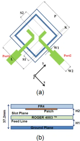
The novel dual-polarized slot-coupled patch antenna fed through a square ring slot is shown in Figure 1.2. It is apparent that the layout is symmetric with respect to the two input ports. The latter represents a useful feature when designing a wideband dual-circular polarized patch (requiring an additional feeding circuit to generate two signals with the same amplitude and a 90° phase shift), or when designing the feeding network of a dual-polarized array.
Figure 1.2 - (a) Top view and (b) stackup of the square patch fed through a square ring slot. Dimension of the geometrical parameters for a WIMAXTM antenna: P=20.5mm, L=16.3mm, K=0.5mm, W1=2.5mm,
It is worth noting that, in dual-polarized patch antennas, geometrical and electrical symmetry are advantageous in improving port isolation and cross-polarization performance.
To show the working principle and the radiation properties of the proposed slot-coupled patch, a sample antenna operating at the 3.3-3.8 GHz WIMAXTM frequency band has been designed, fabricated and characterized. Nevertheless, it is apparent that the proposed geometry can be used for any application where a planar dual-polarized antenna with a port isolation greater than 20dB and a fractional bandwidth greater than 10-15% is required (larger impedance bandwidths can be obtained by adding a square stacked patch).
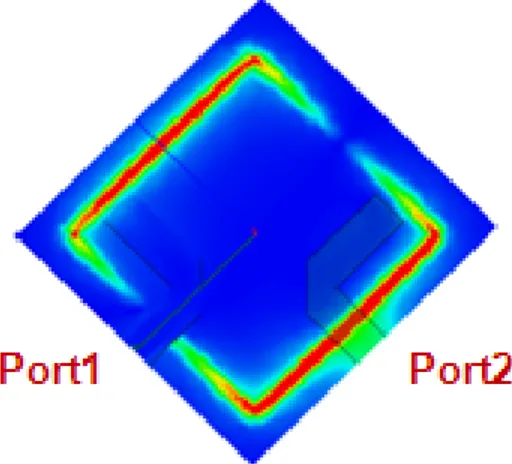
In the sample antenna, both microstrip lines are printed on the same 1.524mm thick Rogers RO4003 substrate (εr=3.55, tgδ=0.0027), which is 70x70 mm2 square. The square ring slot has a perimeter of 65.2mm and is etched on the other side of the above substrate, namely on the metallic ground plane separating the feed lines from the square patch. As in other slot-coupled patch configurations, the length of the open-circuited stub behind the slot is optimized for input impedance tuning. A 100x100 mm2 square aluminum reflector is placed at a distance of 22mm from the feed lines, to reduce back radiation and increase the antenna gain. The 20.5x20.5 mm2 copper patch is printed on the bottom layer of an FR4 laminate, which is 1.6mm thick and 60x60 mm2 wide (it also acts as a cover for the antenna). The air gap between the patch and the slot plane is 11mm thick. Figure 1.3 illustrates the electric field distribution inside the square ring slot when port 1 of the patch in Figure 1.2 is fed. It is apparent that the field distribution resembles that of the fundamental resonating mode of a ring slot. This is in agreement with the fact that the slot perimeter is close to the guided wavelength λg of a slotted line with the same geometrical and electrical parameters as those of the slot: λg=66mm, at 3.5GHz.
The electric field distribution shown in Figure 1.3 reveals a number of interesting features.
Figure 1.3 - (a) Direction and (b) amplitude of the electric field inside the square ring slot, when port 1 of the antenna in Figure 1.2 is fed (HFSS data).
The side of the ring slot that is directly fed and the one parallel to it are both excited, and the electric fields induced into the two slot-sides are in phase and with a similar amplitude; as a consequence, due to above phase relationship and the symmetric position of the above the sides with respect to the patch centre, the resonant mode of the patch (that one associated with port 1) is properly excited and low cross-polarization is expected.
Moreover, the electric field distribution induced into the two sides of the slot orthogonal to the previous ones are out of phase and do not excite the orthogonal resonant mode of the patch (that one associated to port 2). Finally, the induced electric field does vanish close to the centre of the above sides of the slots; it means that relatively high port isolation is expected when that point is used to couple the slot ring to the feed line of port 2.
It is worth noting that since the slot perimeter is less than the free-space wavelength (actually it is around a slot-line guided wavelength) and the patch perimeter is almost double the free-space wavelength, the whole square ring slot always remains under the patch, for any design frequency. Moreover, due to the symmetry between the two ports, the two corporate feed networks of a dual-polarized array can be identical, and the same radiation patterns and gain for the two ports are expected in the whole antenna frequency bandwidth.
The novel layout presented here can be seen as an advancement of the modified “L” configuration presented by Shafai et al. in [42] (the configuration named as “O” in Figure 1.1). Indeed, it is apparent that the 4-slot arrangement in the “O” configuration, which is symmetric with respect to the patch centre, resembles the ring slot geometry. The significant difference is that in the novel configuration all four sides of the ring slot contribute effectively and correctly to the excitation of the two orthogonal fundament patch resonant modes, while in the “O” configuration two slots are just parasitic slots used to minimize the cross-polarization level (also, amplitude and phase of the parasitic slot contribution cannot be easily controlled in the design phase).
1.2.3
Numerical and Experimental Results
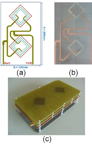
In this paragraph, HFSS simulation results will be compared with measurements carried out on a prototype of the WIMAXTM patch antenna. The antenna prototype is shown in Figure 1.4, and it has been measured in the anechoic chamber at the Department of Electrical Engineering of the University of Oviedo.
Figure 1.4 - Photo of an antenna prototype.
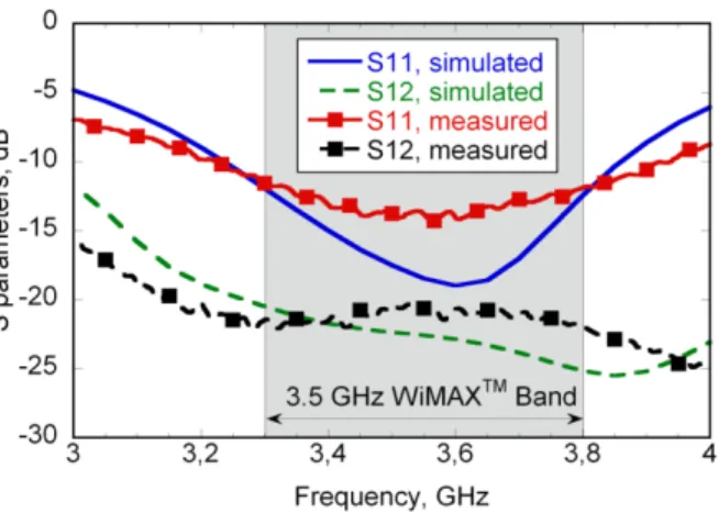
Both measurement and simulation results for the reflection coefficient and port isolation are shown in Figure 1.5, and they exhibit a reasonable agreement.
For both polarizations, the reflection coefficient is less than -10dB, from 3.3GHz to 3.8GHz (percentage impedance bandwidth is 14%). The port isolation is greater than 20dB in the whole WIMAXTM frequency band.
Figure 1.6 - Simulated S-parameters of the square ring slot fed patch as a function of the slot width, L.
Figure 1.7 - Simulated S-parameters of the square ring slot fed patch as a function of the slot width, k.
Figure 1.6-7 show the most significant results of a numerical parametric analysis. Reflection coefficient and port isolation are plotted in Figure 1.6-7 as a function of slot
perimeter and width, respectively (while all other parameters are as those given in the paragraph 1.2.2). Performance dependence on other antenna geometrical parameters (as for example, patch size, stub length, layer thickness, etc.) is comparable to that already discussed in most of the papers relevant to the configurations shown in Figure 1.1.
In Figure 1.6 we can observe that the optimal value of L (edge of the slot, shown in Figure 1.2) is 15.8 mm. Indeed, in this case reflection coefficient is always well below -10 dB in the 3.3-3.8 GHz band; moreover slot and patch resonant-frequencies are positioned in order to create a single large bandwidth. When L is increased from 15.8 mm to 16.8 mm and then 17.8 mm, the slot resonant-frequency moves toward lower frequencies. For the last two values, S11 curves present two separate resonance peaks.
Moreover, as can be seen from Figure 1.6, the patch resonance frequency remains unchanged at around 3.65 GHz. For all considered values of L, port isolation remains greater than 20 dB in the 3.5 GHz WIMAXTM band. In Figure 1.7, the numerical results of a parametric analysis with respect to the slot width (k parameter in Figure 1.2) are shown. The reflection coefficient is almost constant for values of k greater than 0.5mm. For k<0.5 mm worse performance is obtained. The isolation is greater than 20 dB until k is less than 0.5 mm.
Although the achieved port isolation is not as high as that obtained for “T” configurations [43]-[45], it is worth mentioning that even for a high performance slot-coupled single patch the port isolation reduces to less than 25dB [43] when the latter is arranged in antenna arrays, due to the mutual coupling effects.
To show the robustness of our solution in terms of port isolation performance, a small 2x2 array (Figure 1.8) has been designed and it has been verified that the port isolation for the array is still greater than 20dB as for the single element.
To better investigate the properties of the electric field distribution along the ring slot of the designed antenna, the simulated S12 parameter has been calculated when the
square patch is removed. From the numerical results in Figure 1.9 it is apparent the port isolation dips at around 3.6GHz, which was expected on the basis of the discussion in the paragraph 1.2.2.
Figure 1.8 - (a) Comparison between the isolation of the dual-polarized single element in Figure 1.2 and that one of the dual-polarized 2x2 array shown in
Figure 1.9 - Simulated S12 parameter of the square ring slot fed patch in Figure 1.2, when the patch has been removed.
It can be stated that the degraded isolation performance is due to a patch-induced coupling between the two orthogonal modes. On the other hand, it is worth mentioning
that by properly optimizing antenna parameters, a higher isolation could be obtained for those applications where a reduced impedance bandwidth can be accepted.
Figure 1.10 - Measured and simulated co-polar and cross-polar components for the square slot fed patch in Figure 1.2, at f=3.55 GHz when port 2 is fed: (a) =45° plane and (b) =-45° plane.
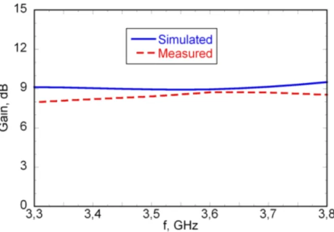
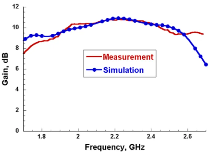
In Figure 1.10, the co-polar and cross-polar components of the radiation pattern, in the φ=45° and φ=-45° radiation planes, are shown, when port 2 is fed. The measured half power beamwidths at 3.55 GHz is around 56° in both principal planes, and cross-polar components are below -18dB at the broadside direction. The measured gain is between 8dB and 8.7dB in the band of interest (Figure 1.11). Similar results are obtained when port 1 is fed. Finally, we verified that the main beam is not depointing and the radiation pattern is almost symmetric, in an extended frequency range; this is as expected since the phase centre is the same for the square slot and the patch [46].
Figure 1.11 - Measured and simulated gain of the square ring slot fed patch in Figure 1.2, when port 2 is fed.
1.2.4
Conclusions
A novel slot-coupled patch fed through a square ring slot has been presented and design criteria have been discussed. Due to its simple structure, the patch described here can be used as the radiating element of medium and large planar arrays with dual linear polarizations (vertical/horizontal polarizations or ±45° slanted polarizations). Antenna performance has been shown by the design, fabrication and characterization of a patch operating at the 3.3-3.8 GHz WIMAXTM frequency band. A port isolation of 20dB has been obtained, in a 500MHz frequency band (14% fractional bandwidth), with cross-polar level less than -18dB in the broadside direction. On the other hand, different geometrical parameter sets could be determined with reference to different specifications; in particular, we found that the final design of the proposed solution is a result of a trade-off between frequency bandwidth enlargement and isolation improvement. With respect to other slot-coupling feeding techniques for dual-polarized patch antennas, the configuration here proposed exhibits a simple structure and a valuable symmetry property with respect to the two feeding ports, while preserving a
satisfying isolation between the two input ports. Moreover, only one feeding network laminate is required, and the level of the coupling between the patch and the feeding line is increased with respect to configurations using (for each polarization) only one rectangular slot shifted with respect to the patch centre. Impedance bandwidth enlargement can be achieved by adding either stacked patches or other parasitic elements close to the main radiating patch, while preserving the original symmetry properties. Finally, due to the symmetry of the antenna layout with respect to the two feed ports, good axial-ratio performance can be obtained when it is used to radiate a circularly polarized field, as shown in [5] and [6], where a single feed and a double feed technique have been used, respectively.
1.3 A wideband slot-coupled stacked-patch array
for wireless communications
1.3.1
Introduction
Recently some frequency bands have been assigned to upcoming wireless applications to guarantee the Broadband Wireless Access (BWA) together with traditional cellular and Local Area Network (LAN) services. Among them, the frequency band from 2500MHz to 2690MHz has been assigned to 3G mobile UMTS (Universal Mobile Telecommunications System) as an expansion band of the 1920-2170 MHz UMTS band. Moreover, the frequency band from 2300MHz to 2700MHz is reserved to WIMAX™ applications in some areas of the north and South America and in the all Asia. The newest installations of base station antennas have to afford the need to provide the area coverage for all above services and in this context it is preferable to avoid using one antenna for each system. For service systems, wideband or multi-band antennas are needed when the lack of space is a determinant constraint or when buildings cannot be defaced by multiple antenna installations. Actual radiating systems provide multi-band operability for GSM and UMTS cellular services, with a maximum percentage bandwidth up to 25%. In addition to the multi-band element need, the antenna system is often requested to provide dual polarization capability. This is necessary to implement diversity at the base station, to compensate for the signal degradation due to multipath phenomena [47]. Diversity consists in using multiple antenna systems that receive two sufficiently uncorrelated copies of the signal and properly combine them at the receiver to increase the signal reliability. A multiple antenna system for diversity techniques that provides two uncorrelated received signals needs two input ports, which can be realized with two antennas placed at a certain
distance (spatial diversity) or with complementary radiation patterns. A space saving solution is gained with polarization diversity [48]. Much attention has been given to polarization diversity through analytical and experimental investigation, resulting in the observation that ±45° slanted polarizations are preferred to vertically/horizontally (V/H) polarizations because they form identical patterns in the azimuth plane and they are equally sensible to horizontally and vertically polarized signals.
This project proposes a two-element linear array of dual polarized wideband stacked patches fed through a novel slot coupling technique [2], where the patch is coupled to the feeding line through a square ring slot. The implementation of a sequential rotation technique and the symmetry properties of the slot-patch pair guarantee good performance in terms of the isolation between the two polarization ports and the level of the cross-polar components in both principal radiation planes. A single layer laminate is needed for the feeding network, since the square ring slot can be excited through two orthogonal non-overlapping microstrip lines. The final array operates in the GSM 1800-1900 band (1710 – 1910 MHz), UMTS band (1920 - 2170 MHz), ISM band (2400 - 2484 MHz) and UMTS 3G expansion band (2500 - 2690 MHz) or, alternatively, WIMAX™ band (2300 – 2700 MHz). The antenna has been designed and optimized by using Ansoft HFSS™. A prototype has been realized and measurements were carried out showing good performance in the whole required bandwidth (45% bandwidth, Reflection Coefficient < -10dB)). Simulated and measured results are shown for reflection coefficient, port isolation, antenna gain, and radiation patterns in the antenna principle radiation planes.
1.3.2
Antenna Design
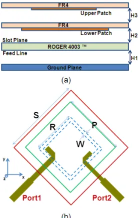
Figure 1.12 shows the stack-up and the layout of the wideband slot-coupled stacked-patch array, together with the two feeding lines. A metallic reflector is needed to limit the back radiation and increase the antenna gain. Since the layout is symmetric with respect to the two input ports, identical radiation and input impedance properties are expected for the two ports.
Figure 1.12 - Stack-up and top-view geometry of the wideband slot-coupled stacked-patch (H1 = 22mm, H2=10mm, H3 = 11mm, S = 45mm (lower plane), P = 35mm (upper plane), R =31mm (slot side), W =
Both microstrip lines are printed on the lower side of a 1.524mm thick RO4003 Rogers substrate (εr=3.55, tgδ=0.0027). The square ring slot has a perimeter of 124mm,
a 0.5mm width, and it is etched on the upper side of the above substrate, i.e. on the metallic ground plane separating the feeding lines from the lower square patch. As in other slot-coupled patch configurations [33], the ground plane prevents spurious radiation from the feeding network, and the length of the open-circuited stub behind the slot is optimized for input impedance tuning. The 45x45mm2 lower patch is printed on the bottom layer of an FR4 laminate, which is 1.6mm thick; the upper 35x35mm2 stacked patch is printed on the bottom layer of another FR4 laminate, which also acts as an antenna cover. The air gap between the slot plane and the lower patch, and that one between the driven patch and the stacked patch is 10mm and 11mm high, respectively.
By referring to port 2, the side of the ring slot that is directly fed and that one parallel to it (i.e. the -45° slanted sides of the ring slot shown in Figure 1.12b) are both excited, and the electric field induced into the two slot-sides are in phase and with a similar amplitude; as a consequence, due to above phase relationship and the symmetric position of the -45° slanted sides with respect to the patch centre, the fundamental resonant mode of the patch (that one associated to port 2) is properly excited and low cross-polarization level is expected. Moreover, the electric field distribution (Figure 1.13) induced into the two sides of the slot orthogonal to the previous ones (i.e. the +45 slanted sides of the ring slot shown in Figure 1.12) are out of phase and do not excite the orthogonal resonant mode of the patch (that one associated with port 1).
Finally, the induced electric field does vanish close to the centre of the -45° slanted sides of the slots; it means that a good port isolation is expected when that point is used to couple the square slot to the orthogonal feed line corresponding to port 1. The previous characteristics are apparently related to the fact that the square ring slot is resonating at the design frequency.
Two radiating elements are lined in a column with a separation equal to 100mm (0.9λ@2.7GHz). The overall size of the array panel is 125x200mm2 and it is 45mm thick, giving the antenna a relatively low profile design. A 50 Ω microstrip line feeds both two elements of each column through one power divider for each polarization.
Starting from the feeding point, a 50Ω microstrip feeding line is transformed to a 25Ω one by a quarter-wavelength impedance matching line located just before the power divider. Quarter wavelength transformers are 24mm long and 6mm wide. To improve polarization purity and port isolation, the novel slot-coupling feeding technique has been combined with a sequential feeding technique [2] as suggested in [50]-[51]. Due to the symmetry of the antenna/slot configuration, the 90° rotation required by the sequential feeding technique does not apply to the radiating patches, but slight modifications are required at the feeding network level only.
Figure 1.13 - Electric field distribution induced into the two sides of the slot when port 2 is fed.
1.3.3
Numerical and Experimental Results
Figure 1.14 shows the realized prototype and the corresponding layout. The 2x1 sub-array prototype (Figure 1.14c), was realized on a 125mm wide and 200mm long laminate with the same stack-up as in Figure 1.12a.
Figure 1.14 - Realized prototype of the wideband slot-coupled stacked-patch array. (a) Simulated 2x1 subarray. (b) Detail of feeding lines and coupling slots. (c) Realized 2x1 prototype.
The sequential rotation technique applies here only to a 2 port sub-array and its effect is consequently reduced with respect to a longer 2Nx1 array where better performance are expected. Reflection coefficient is less than -10dB in the whole frequency band from 1.71GHz to 2.69GHz, as shown in Figure 1.15, where a good agreement is visible between simulation results and measurements data except for a small difference due to imprecision in the prototype realization.
Figure 1.15 - Simulated and measured reflection coefficient for the wideband slot-coupled stacked-patch array.
Figure 1.16 - Simulated and measured isolation for the wideband slot-coupled stacked-patch array.
The overall impedance percentage bandwidth (Reflection coefficient<-10dB) is greater than 45%. Both numerical and measured data are slightly different for the two ports because of some differences in the corresponding feeding lines mainly due to the sequential rotation technique applied to the +45° polarization microstrip line. The array port isolation, shown in Figure 1.16, is greater than 22dB in the whole frequency band of interest.
Figure 1.17 and Figure 1.18 show the co-polar and cross-polar components of the radiation patterns, at 2.2GHz, in the azimuth (φ = 0) and elevation (φ = 0) planes, respectively, when port 1 is fed.
Figure 1.17 - Copolar and crosspolar radiation pattern in the azimuth plane for the wideband slot-coupled stacked-patch array, at 2.2 GHz when port 1 is fed.
Figure 1.18 - Copolar and crosspolar radiation pattern in the elevation plane for the wideband slot-coupled stacked-patch array, at 2.2 GHz when port 1 is fed.
The relative amplitude of the cross-polar components is less than -20dB. Half Power Beam Width (HPBW) is 61° in the azimuth plane and 36° in the elevation plane. The antenna gain for Port 1 (Figure 1.19) is between 8dB and 11dB in the entire band of interest. Similar results have been obtained for the orthogonal polarization (when port 2 is fed).
Figure 1.19 - Simulated and measured gain for the wideband slot-coupled stacked-patch array (when Port 1 is fed).
In Table 1.1 - Gain and HPBW for the wideband slot-coupled stacked-patch array. HPBW and antenna gain are summarized in Table 1.1.
Frequency, MHz Gain, dB HPBW, deg
(Horizontal Plane) 1800 8.7 60° 2050 10.4 61° 2400 10.4 57° 2500 9.5 56° 2600 9.3 55°
Table 1.1 - Gain and HPBW for the wideband slot-coupled stacked-patch array. We can observe that the HPBW in the horizontal plane is quite stable in the whole antenna operating band.
1.3.4
Conclusions
A 2x1 array module of wideband dual-polarization stacked-patch antennas working between 1.71GHz and 2.69GHz (percentage bandwidth greater than 45%) has been described in this paragraph. The array is intended as a module for any 2Nx1 linear array to be composed on the basis of gain requirements for base station antennas. The radiating elements are fed through a novel slot coupling technique and a sequential feeding technique has been implemented for each patch pair. As a result, good isolation and cross-polarization purity performance are obtained, as required by the specifications for dual-polarization base station antennas. Array performance was analyzed by numerical simulations and a prototype was realized. A measurement campaign was conducted to evaluate reflection coefficient, isolation, radiation patterns and antenna gain. Simulated and experimental results are in quite good agreement and they exhibit low crosspolar components and a relatively high isolation.
1.4 A Circularly Polarized 2x2 Array
1.4.1
Introduction
In microwave radio links, circular polarization is able to reduce multipath effects. It also allows more flexible reciprocal orientations between the transmitting and the receiving antennas. For the above reasons, circularly polarized (CP) antennas are used in a number of communication systems, as for example GPS (Global Positioning System) terminals and satellite-to-mobile wideband communication links, as well as UHF RFID (Radio Frequency IDentification) readers. Moreover, a number of ATC (Air Traffic Control) radars and SAR (Synthetic Aperture Radar) systems adopt CP antennas, exploiting some interesting properties of the polarimetric scattering. CP patch antennas are generally divided into two categories, named as single-feed and dual-feed configurations. Both these configurations are able to excite the patch orthogonal principal modes with a quadrature phase shift. Dual-feed layouts resort to an external power splitter (for example a reactive power divider or a 90° quadrature hybrid). On the other hand, single-feed configurations are based on a single feed and perturbation segments that are applied to the patch boundary. Typical single-feed configurations are the corner truncated patch and the nearly square patch with the feeding point located along the patch axes or diagonals. Single-feed solutions are simpler but exhibit a limited Axial Ratio (AR) bandwidth [52]. On the contrary, the dual-feed technique results in a larger AR bandwidth [39], [53] at the expense of a more complex feeding network, which is a substantial drawback in electrically large array antennas.
In the paragraph 1.4.2, a patch antenna using a novel slot-coupling technique (firstly introduced in [2] for dual-linear polarization patch antennas) is used to realize a CP 2x2 array with wide impedance matching and AR bandwidths. Specifically, a dual-feed
technique is used for each array element, and it is combined with a sequential rotation array feeding technique [54]-[56]. The sequential rotation technique consists in sequentially rotating each patch element together with imposing an appropriate offset in the feed excitation phase. Sequential rotation feeding can be used to improve cross polarization (circular polarization purity), radiation pattern symmetry and impedance bandwidth, also providing improved port isolation in dual-circular polarization arrays [49]. Numerical simulations obtained with Ansoft DesignerTM are used to show the remarkable AR performance of the 2x2 array. The above described improvements are obtained at the cost of a moderately increased feeding network complexity. Numerical results are validated through comparisons with measurements performed on an array prototype.
1.4.2
Antenna Design and Experimental Results
2x2 square array with an inter-element distance equal to 72mm (about 0.85λ0, where
λ0 is the free space wavelength at the centre of the WIMAXTM frequency band) has been
analyzed in this paragraph. Preliminary numerical results have been obtained by feeding each array element with an ideal 90° phase shifter (in the numerical tool, Port1 and Port2 of the (n,m) array element have been fed with an input current equal to In,m and
In,mexp(+j/2), respectively). The radiating element has been used in a conventional 2x2
array (In,m=1, with n=1,2 and m=1,2) and later on in a 2x2 sequentially rotated array
(I1,2=exp(+j/2)I1,1=-I2,1, I2,2=-I1,1, and each patch is 90° rotated with respect to the
adjacent one): in both cases the array was constituted by four patches and four ideal 90° phase shifters. The use of ideal phase shifters instead of a microstrip feeding network allows us to avoid AR performance degradation due to phase shift errors in the element feeding currents; nevertheless, mutual coupling between array patches is still accounted for. The conventional 2x2 array (where the four array elements are fed in-phase) exhibits very good AR performance with respect to both frequency and angular
deviation from broadside direction, θ. From the numerical results shown in Figure 1.20, it results that the simulated AR at the broadside direction is less than 2.25dB in the whole frequency band, and its variations within the array beam are less than 0.5dB, in both principal radiation planes at =0° and =90°. Such a good performance is in some way related to the symmetry properties of the novel slot-coupling feeding technique [2].
Figure 1.20 - AR for a 2x2 conventional array (without sequential rotation) and with ideal phase shifters (without microstrip feeding network). AR is plotted vs. the angular displacement from broadside, θ, for different frequency values (3.3GHz, 3.55GHz and 3.8GHz), and in both principal radiation planes (=0° and
=90°).
Simulation results also showed a stable half-power beamwidth (HPBW), versus frequency, in both principal planes. Indeed, we observed a HPBW of 32° at the central frequency, 3.55GHz, with variations of less than 2° in the WIMAXTM frequency band. The array gain is about 13dB in the broadside direction (θ=0°). When the four array elements are sequentially 90° rotated and fed with a proper phase shift, as required by the sequential rotation technique, the same performance in terms of HPBW and gain is obtained as for the conventional 2x2 array. On the other hand, it is apparent from the results in Figure 1.21 that the AR at broadside becomes less than 0.03dB over the whole WIMAXTM frequency band. Moreover, AR variations with respect to the angle θ are
less than 0.5dB, in the whole frequency band and in both the =0° and the =90° radiation planes.
Figure 1.21 - AR for a 2x2 array with sequential rotation and with ideal phase shifters (without microstrip feeding network). AR is plotted vs. the angular displacement from broadside, θ, for different frequency values
(3.3GHz, 3.55GHz and 3.8GHz), and in both principal radiation planes (=0° and =90°).
Figure 1.22 - Layout of the 2x2 sequentially rotated CP array.
Above results confirm that the sequential rotation technique can significantly improve AR performance, giving an improvement of about 2dB with respect to the
conventional 2x2 array. Finally, a sequentially rotated 2x2 array with a complete microstrip feeding network has been designed, as shown in Figure 1.22. Each dual-linear polarized patch has been fed through a reactive 3dB power divider that includes two microstrip lines whose lengths differ of λg/4, where λg is the microstrip wavelength
(λg=52mm, microstrip wavelength at 3.55GHz).
The power divider also includes a quarter-wavelength impedance transformer (6mm wide and 12.6mm long microstrip line). The feeding network consists of microstrip lines whose lengths have been adjusted to achieve the required 90° current phase difference between adjacent elements. A prototype of the array has been fabricated and a photo is shown in Figure 1.23.
Figure 1.23 - A prototype of the 2x2 CP array.
The reflection coefficient for the 2x2 CP array is shown in Figure 1.24.
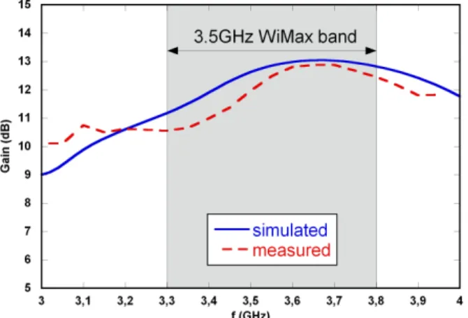
It is apparent that the measurements and the numerical data are in a very good agreement; except for a frequency shift which has been often noted when using an electromagnetic tool that considers infinite dielectric layers. In the whole WIMAXTM frequency band, the measured reflection coefficient is less than -10dB. As apparent from Figure 1.25, the maximum measured gain is about 12.8dB.
Figure 1.24 - Simulated (solid line) and measured (dashed line) reflection coefficient for the 2x2 CP array in Figure 1.23.
Figure 1.25 - Simulated (solid line) and measured (dashed line) broadside gain vs. frequency for the 2x2 CP array in Figure 1.23.
Figure 1.26 illustrates the simulated and measured array radiation patterns, in the =0° plane, at 3.55GHz. The antenna radiates a Right Hand Circular Polarization (RHCP) and the measured cross-polar component (LHCP, Left Hand Circular Polarization) is less than -20dB within the HPBW which is equal to 28° (a little bit smaller than the simulated one which is equal to 32°).
Figure 1.26 - Simulated (solid line) and measured (dashed line) normalized radiation pattern for the 2x2 CP array in Figure 1.23, in the φ=0° principal plane, at 3.55GHz: RHCP (without markers) and LHCP (with
markers).
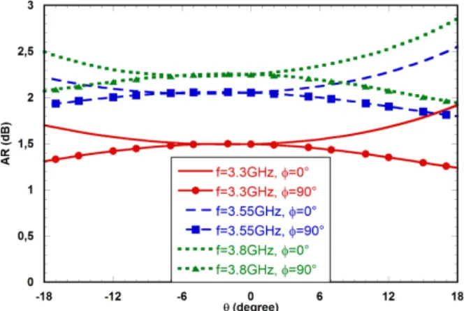
The measured and simulated AR, versus the frequency and the angle from broadside are shown in Figure 1.27 and Figure 1.28, respectively. In the broadside direction, the measured AR is less than 1.35dB in the whole WIMAXTM frequency bandwidth, and the 3dB AR bandwidth is of about 30%. The measured AR is less than 2.25dB at the centre frequency (3.55GHz), for any direction within the array main beam, and in both the =0° and the =90° radiation planes.
Figure 1.27 - Simulated (solid line) and measured (dashed line) Axial Ratio vs. frequency for the 2x2 CP array in Figure 1.23 (at the broadside direction, θ=0°).
Figure 1.28 - Simulated (solid line) and measured (dashed line) Axial Ratio vs. the θ angle, for the 2x2 array in Figure 1.23, at the centre frequency (3.55GHz) and in both principal planes: φ=0° (without markers) and
φ=90° (with markers).
1.4.3
Conclusions
A dual-feed square patch coupled to the microstrip feeding line through a square ring slot has been used to realize a circularly polarized 2x2 array. To obtain a wide impedance bandwidth as well as a wide axial ratio bandwidth a sequential rotation feeding technique has also been adopted. Simulation and measurement results for an array designed to operate in the WIMAXTM frequency band have shown that both an AR<3dB and a return loss greater than 10dB can be obtained. In particular, the measured 3dB AR percentage bandwidth results to be as high as 30%.
Chapter II
2 D
UAL
-B
AND
PIFA
FOR
W
IRELESS
C
OMMUNICATIONS
S
YSTEMS
2.1 Introduction
In recent years, specific attention has been focused on terrestrial high definition television services and applications. The DTV (Digital TeleVision) and the European DVB-T (Digital Video Broadcasting-Terrestrial) standards are rapidly becoming very popular and they are nowadays the only terrestrial television service available in many regions [58]. Next generation terminals will be required to have an integrated antenna in order to avoid cabled connections and to render them relatively portable (at least within an indoor scenario). In addition to this, a web access through a Wireless Local Area Network (WLAN) could be provided to guarantee access to on-demand services. Therefore, dual-band compact integrated antennas for DVB-T and WLAN applications represent a valuable solution.
A number of DTV wideband antennas have been recently presented [59]-[65], which are mainly low cost and low profile and of easy fabrication printed monopoles and patch-alike antennas. Printed monopoles require a careful positioning inside devices with high circuitry density, as they are quite sensitive to the presence of close by metal
parts. On the other hand, patch-alike antennas and PIFAs are suitable for integration because their ground plane also acts as a shield.
In this communication, a dual-band PIFA operating in both the DVB-T (470–862 MHz, 59% percentage bandwidth [58]) and the WLAN (2400-2484 MHz, 2.7% percentage bandwidth) frequency bands is presented, which is suitable to be integrated into devices, such as a monitor or a TV chassis, where relatively large volumes are often available along their sides or top. The proposed solution exploits the working principle recently proposed for an UWB PIFA [66], which is characterized by a driven (fed) radiating element separated by a small gap from a coplanar parasitic branch. In [66], the driven PIFA element acts as the primary element, governing the lowest resonant frequency, while the higher resonant frequency is controlled by the parasitic element. The proper dimensioning of the driven and parasitic branches and of the separating gap allowed us to get a compact dual-band antenna design. The extent of the antenna proposed in [66] was also reduced. In modern displays, the available volume in a monitor chassis has a transverse area usually less than 15mmx10mm, while almost its entire border length is accessible. Consequently, in this work, it was assumed that a volume less than 250 x 15 x 10 mm3 should be occupied by the radiating element.
2.2 Compact Dual-Band PIFA for DVB-T and
WLAN Applications
2.2.1
Introduction
DVB-T PIFAs have been recently proposed [67]-[68]. In [67], the radiating patch and the ground plane are not facing each other, as it happens in conventional PIFAs, but they are orthogonal. This could result in high coupling with the circuitry, if the latter results to lie in close proximity. The antenna structure proposed in [68] looks more as a multi-antenna system (two radiating elements are separately fed and coupled to a third parasitic one). The PIFA here proposed is electrically smaller than the element in [68], where the parasitic patch and a wide ground plane increase the entire antenna volume. In addition, it offers dual-band functionality as it operates also in the 2.4 GHz IEEE 802.11b,g WLAN band, so that a single antenna can guarantee access to both TV and internet services, while simplifying terminal chassis design. To the best of authors’ knowledge, dual-band radiating elements for DVB-T and WLAN applications have not been proposed yet.
The proposed PIFA layout is presented in the paragraph 2.2.2, where numerical data and experimental measurement results on two prototypes are also shown. In particular, the robustness of the solution in terms of antenna impedance matching against detuning effects that can be caused by the presence of surrounding metal parts is discussed.
2.2.2
Antenna Design and Experimental Results
Figure 2.1 shows the layout of the proposed PIFA and Table 2.1 summarizes its main dimensions. The layout resulted from an optimization process focused to reduce the overall antenna dimensions as much as possible.
Figure 2.1 - Geometry and prototype of the proposed dual-band PIFA (the SMA connector model is also shown). L 207 M 10 W 12 B 133 H 8 N 10 S 5 D 51 A 69 F 10
Table 2.1 - PIFA dimensions (MM)
The antenna is cut from a single metal sheet (even the trapezoidal feed plate is part of it) in the required planar geometry/shape and then it is properly bent to obtain the
final 3D structure. This simplifies the industrial fabrication and avoids any soldering, except for that at the antenna connector.
Similarly to the antenna in [66], the proposed PIFA is characterized by a driven radiating element separated by a small gap from a coplanar parasitic branch. The driven PIFA element acts as the primary element, governing the lowest resonant frequency, while the upper resonant frequency close to the DVB-T band is controlled by the parasitic element. Moreover, the separating gap helps in controlling a third resonance around 2.45 GHz in the IEEE 802.11b,g band for WLANs. Thus, as an improvement of the solution in [66], the proposed PIFA exhibits a dual band functionality. Moreover, if compared with [66], a significant reduction of 63% and 87% was achieved for the electrical thickness (H) and width (W), respectively (the electrical size is referred to the wavelength at the DVB-T band centre frequency, where λ=448mm) at the cost of only 9% length (L) increase.
The linear PIFA occupies an overall volume of 207 x 12 x 8 mm3. This radiating element is relatively large with respect to antennas printed or mounted on high permittivity substrates but, at the same time, it can guarantee higher gains and efficiencies.
Figure 2.2 - Simulated reflection coefficient for the proposed dual-band PIFA.
As shown in Figure 2.2, the reflection coefficient is below -6 dB in the whole DVB-T band, and less than -10 dB in the IEEE 802.11b,g band.
The above values are typical thresholds for integrated antennas for such communication standards. It is worth noting that wideband performance in the DVB-T band (59% percentage bandwidth) is achieved through a careful tuning of two distinct main resonances. On the basis of a parametric analysis, the main parts for the antenna optimization were identified. The driven and parasitic elements jointly contribute to determine the two resonances at the DVB-T band. They can be controlled by varying the W, H and L parameters.
Figure 2.3 - Simulated reflection coefficient of the proposed dual-band PIFA as a function of frequency for different values of ∆S.
Figure 2.3 shows the reflection coefficient behaviour with respect to frequency for different values of ∆S between -3 mm and 3 mm (see Figure 2.3 for ∆S meaning). The gap S between the two elements, mainly affects the antenna reflection coefficient at the IEEE 802.11b,g band.
The reflection coefficient is plotted in Figure 2.4 and Figure 2.5 for different values of the M and N parameter, respectively. It is worth noting that these parameters affect the reflection coefficient values both in the IEEE 802.11 and in the DVB-T bands. Indeed, M and N variations cause the resonant frequency to shift in the IEEE 802.11b,g band and the reflection coefficient values to increase at the DVB-T frequencies. In particular, it is observed that M and N values greater than 10mm determine similar
performances in terms of reflection coefficient values and this minimum value is obviously preferred in order to minimize the total volume of the antenna. By varying the feed distance from the short-circuit, D, no effects are visible in the DVB-T band. However D is effective for fine tuning at 2.4 GHz. The parameter A affects both the resonance in the WLAN band and the second of the two resonances in the DVB-T band.
Figure 2.4 - Simulated reflection coefficient of the proposed dual-band PIFA as a function of frequency for different values of the parameter M.
Figure 2.5 - Simulated reflection coefficient of the proposed dual-band PIFA as a function of frequency for different values of the parameter N.
The gain and the radiation patterns in the principal planes (co-polar and cross-polar components) are shown in Figure 2.6-8 for the centre frequencies of the bands of interest.
Figure 2.6 - Simulated gain for the proposed dual-band PIFA in the DVB-T band.
Figure 2.7 - Simulated gain for the proposed dual-band PIFA in the WLAN band.
The antenna gain is between 2.4 dBi and 3.3 dBi in the DVB-T band, and between 4.4 dBi and 4.8 dBi in the WLAN band. Radiation patterns have different shapes in the two frequency bands.
Figure 2.8 - Simulated radiation patterns (components Eθ and Eφ) in the principal planes at 670 MHz (central
frequency for the DVB-T band) and 2440 MHz (central frequency for the IEEE 802.11b,g band) for the proposed dual-band PIFA.
At lower frequencies, in the DVB-T band, the antenna behaves like a dipole with main lobes along broadside directions and nulls in the endfire ones. An omni-directional pattern is observed in the plane transverse to the antenna (yz-plane). At higher frequencies the antenna is electrically longer, high side lobes occur and no main beam can be identified. Cross-polar component levels are always below -18dB in the DVB-T band, while in the IEEE 802.11 band they cannot be distinguished in some planes (see for instance the xy-plane). However, since the terminal where the antenna has to be integrated is often an indoor device operating in a rich multipath environment, radiation patterns are not required to have specific properties in terms of beam width/shape and cross-polar levels.
On the other hand, when the antenna is integrated into the device, radiation patterns would be furtherly deformed, exhibiting higher cross-polar components, by the presence of internal parts of the monitor chassis.
A first prototype (Prot.1) was realized with a 0.4mm thick adhesive copper tape, cut and folded around a 207 mm long, 12 mm wide and 8 mm high polystyrene block (Figure 2.1). Measured reflection coefficients are shown in Figure 2.9, and compared with simulated results. The first prototype (Prot.1) exhibits a WLAN operating band slightly up-shifted with respect to simulation data.