www.nature.com/scientificreports
Multi-Scale-Porosity TiO
2
scaffolds
grown by innovative sputtering
methods for high throughput
hybrid photovoltaics
Salvatore Sanzaro
1,2, Emanuele Smecca
1, Giovanni Mannino
1, Corrado Bongiorno
1,
Giovanna Pellegrino
1, Fortunato Neri
2, Graziella Malandrino
3, Maria Rita Catalano
3,
Guglielmo Guido Condorelli
3, Rosabianca Iacobellis
4,5, Luisa De Marco
6, Corrado Spinella
1,
Antonino La Magna
1& Alessandra Alberti
1We propose an up-scalable, reliable, contamination-free, rod-like TiO2 material grown by a new
method based on sputtering deposition concepts which offers a multi-scale porosity, namely: an intra-rods nano-porosity (1–5 nm) arising from the Thornton’s conditions and an extra-intra-rods meso-porosity (10–50 nm) originating from the spatial separation of the Titanium and Oxygen sources combined with a grazing Ti flux. The procedure is simple, since it does not require any template layer to trigger the nano-structuring, and versatile, since porosity and layer thickness can be easily tuned; it is empowered by the lack of contaminations/solvents and by the structural stability of the material (at least) up to 500 °C. Our material gains porosity, stability and infiltration capability superior if compared to conventionally sputtered TiO2 layers. Its competition level with chemically synthesized reference counterparts is
doubly demonstrated: in Dye Sensitized Solar Cells, by the infiltration and chemisorption of N-719 dye (∼1 × 10²⁰ molecules/cm3); and in Perovskite Solar Cells, by the capillary infiltration of solution
processed CH3NH3PbI3 which allowed reaching efficiency of 11.7%. Based on the demonstrated attitude
of the material to be functionalized, its surface activity could be differently tailored on other molecules or gas species or liquids to enlarge the range of application in different fields.
A bright future of our society is based on the capability of tuning the material properties for beneficial scopes. TiO2–based 1D nanostructures are especially appealing to combine the advantages of exposing large active facets1,2
with good mechanical performances and high electrical conductivity3. All those properties enrich 1D-TiO 2
architectures with a transversal empowering for energy, health, and environment applications, since they can be efficiently used as scaffold for Dye4 and Perovskites Solar Cells5, anodes for Li batteries6, electrodes for water
splitting devices7, materials for biosensors detecting DNA8 or glucose3, scaffold for gas sensing9,10, and scaffold
for photo-catalysis11,12.
Among the possible applications that can take advantage from the use of TiO2 nanostructures having
multi-scale-porosity, DSCs (Dye Solar Cells)13,14 have been pushed to a high level of maturity and, nowadays,
represent an interesting alternative to semiconductors technologies mainly due to the large versatility and the low production cost15,16. Using DSC technologies, the light-to-current conversion efficiency was raised up to
13%17. More recently, hybrid solar cells replacing the dye with hybrid Perovskites (PSC) materials18–22 as
sensi-tizer allowed getting efficiency values as high as 22.1% using advanced mixed perovskites23,24. In the standard 1National Research Council-Institute for Microelectronics and Microsystems (CNR-IMM), Zona Industriale-Strada VIII no. 5, Catania 95121, Italy. 2University of Messina, Department of Mathematical and Computational Sciences, Physics and Earth Sciences, V. le F. Stagno d’Alcontres 31, Messina 98166, Italy. 3Department of Chemical Sciences, University of Catania, V. le Andrea Doria 6, 95125 Catania, Italy. 4Italian Institute of Technology Foundation-Center for Biomolecular Nanotechnology (IIT-CBN) Via Barsanti sn, 73010, Arnesano, Italy. 5University of Salento, Department of Innovation Engineering, Via per Monteroni 73100, Lecce, Italy. 6National Research Council-Institute of Nanotechnology (CNR-Nanotec), District of Technology, Via Arnesano 16, 73100 Lecce, Italy. Correspondence and requests for materials should be addressed to A.A. (email: [email protected])
Received: 18 October 2016 Accepted: 21 November 2016 Published: 21 December 2016
www.nature.com/scientificreports/
scheme of the photo-anode of a DSC4 or PSC18, a mesoporous thin film of nanosized TiO
2 crystals is deposited
on a Transparent Conductive Oxide (TCO), annealed for grains sintering and anatase crystallization (typically at 500 °C), and subsequently imbued with a photoactive dye25–29 or infiltrated with perovskite30. In both cases,
mes-oporous TiO2 in the anatase polymorphism has emerged as the most appropriate choice for cell scaffold15,21,23,31.
The most diffused and versatile way to generate nano-TiO2 architectures is by chemical approaches. They offer a
large plethora of fascinating hierarchical and mesoporous structures32–34 with high infiltration capability.
On the other hand, standard physical growth methods cannot straightforwardly compete with chemical approaches since they have an intrinsic tendency to form compact layers. The advent of modified sputtering methodologies to grow, instead, TiO2 scaffolds with high porosity levels would open the field to high production
throughput as linked to the reproducibility of the materials and to the up-scalability of the processes. A first attempt was provided by Thornton with his semi-empirical model35,36. The Thornton’s model defines a range of
deposition parameters such that the layer structure can be qualitatively tuned from dense to nano-porous. On the basis of this model, the deposition temperature must be taken as low as possible to reduce surface diffusion of the deposited ad-atoms, and the Ar pressure likely high enough to increase the layer porosity. Nonetheless, the pore size is extremely limited. Several attempts were done in the literature in order to increase the TiO2 layer
porosity above the Thornton limit by using sputtering or evaporation approaches which generated cauliflower37,
penniform38 or zig-zag39 structures. Some other attempts were done by GLancing Angle Deposition (GLAD)40
to deposit Ti nanostructures41–43 which requires ex-situ oxidation for TiO
2 reaction; or by using array of template
materials (e.g. polystyrene nano-spheres) to exploit their shadowing effect during TiO2 growth44. They however
lack of process simplification and of a transversal demonstration on the applicative valence of the porous scaffold to largely and deeply infiltrate materials of different size and/or nature to be used for wide-ranging applications. This evidence must be also corroborated by the demonstration of an effective interconnection between the host (scaffold) and the guest (infiltrated materials) to exchange information (e.g. carriers).
In this paper we propose a material with multi-scale porosity ranging from nano- to meso- dimensionalities grown by a modified (up-scalable) sputtering method, and we demonstrate its attitude to be functionalized with species of different nature. To this intent, two photoactive blends, namely TiO2+ dye and TiO2+ perovskite, are
realised, characterised and tested in prototype DSCs and PSCs to provide a proofs-of-concept on the transversal empowering of the material.
Results and Discussion
Grazing incidence-local oxidation (gig-lox) process description.
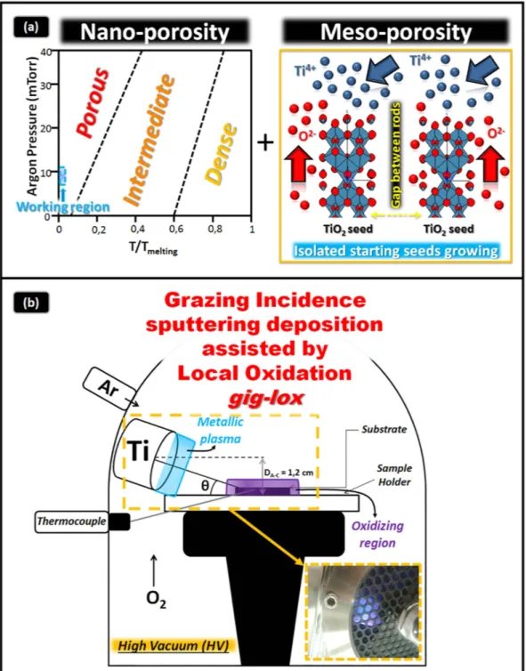
The idea to build the new material is sketched in Fig. 1(a). It is based on the exploitation of a double strategy to provide the material with a dou-ble-range-porosity during growth (in-situ processes).A nano-porosity (1–5 nm) was settled by applying Thornton’s conditions35. Our specific working area is
indi-cated in Fig. 1(a) (left), with the argon pressure raised up to 10.5 mTorr, and the deposition done at room temper-ature to reduce diffusive effects. To reach a higher porosity (> 5 nm) we used a customized sputtering equipment empowered by a Ti off-axis source with an inclination angle θ (Fig. 1(b)) and an oxidizing zone confined at the sample surface, far from the cathode sheath region.
The success in growing a layer with meso-porosity extending through thick layers (e.g. through 1000 nm) mainly resides in the choice of the inclination angle θ (see Supplementary Information Fig. 1S). An optimum inclination angle of 12.7° was identified in our setup as a compromise between the shadowing effect by the start-ing TiO2 seeds (this define the lower limit in θ ) and the verticalization of the Ti flux by increasing θ , that has a
tendency to progressively close the pores by proceeding the deposition. Hereafter we refer to our refined method-ology at inclination angle of 12.7° as gig-lox; the reference process, related to the use of a standard parallel plate geometry in Thornton conditions45, will be indicated by ppg. See methods and SI for more details.
Morphological analyses.
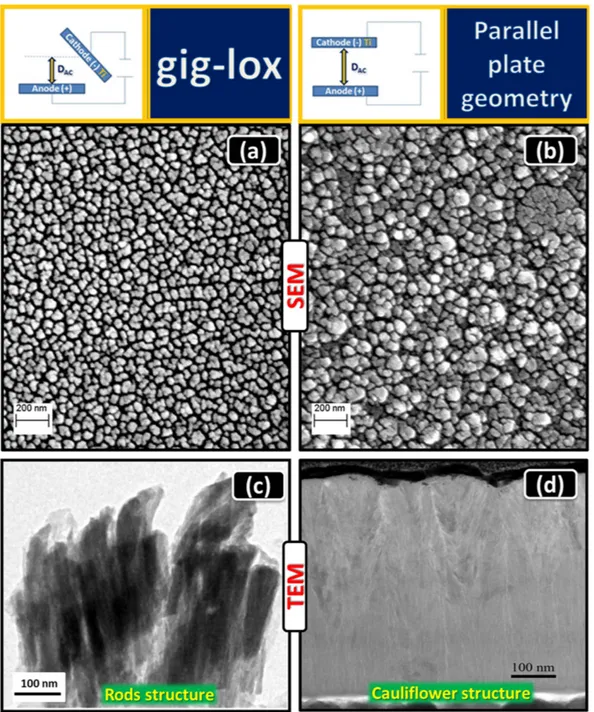
The morphology of the Ti-oxide layers was evaluated by Field Emission-Scanning Electron Microscopy (FE-SEM) in plan-view and cross section configurations (Fig. 2(a,b)). To avoid charging effects, Au nanograins (∼ 5 nm in diameter) were sputtered on the sample surface or section (in some cases they are visible on the sample surface). The as deposited gig-lox layer (Fig. 2(a))is characterized by an array of grains, whose diameter is in the range of ∼ 60–90 nm (Supplementary Information Fig. 2S). For the starting material composition see XPS results in the Supplementary Information, Fig. 3S.The TiO2 grains are surrounded by a network of voids. As counterpart, the as deposited ppg layer, shown in
Fig. 2(b), is made of grains with larger size (∼ 50–150 nm) often aggregated in form of cauliflowers. The TEM cross sections of the two layers are compared in Fig. 2(c,d). The gig-lox layer is made of separated rods extending through the whole thickness. On the other hand, the ppg layer is more compact especially at the bottom half part. The uppermost part has instead a typical cauliflower morphology often reported in the literature37, which
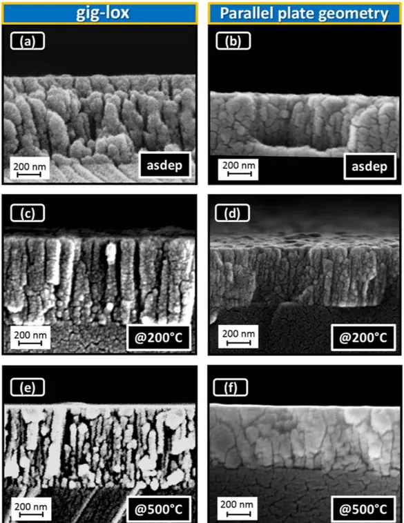
pro-duces a high surface roughness (± 20 nm) in correspondence of the boundaries between adjacent grains. Figure 3a visualizes a rods forest in the as deposited gig-lox layer, with rod diameter in the range of ∼80–90 nm, in agreement with their plan-view (Fig. 2(a)). The rods are separated by ∼10–50 nm large voids extending through the whole thickness (∼ 800 nm). This represents the meso-porosity of the layer. The ppg layer appears, instead, more compact, similarly to what reported in the literature37,45–48. Accordingly, after
ther-mal treatments, grain coalescence causes a shrinkage of the pores in the ppg layer (especially at the surface: see Fig. 3(d,f)). This effect is more pronounced after annealing at 500 °C. On the other hand, the gig-lox layer retains its porosity through the whole thickness with the rod forest architecture still preserved.
Porosity calculation from Ellipsometric measurements.
The TiO2 porosity has been evaluated bySE measurements on ∼ 800 nm-thick samples. The values of n at 550 nm and the layer porosity (see methods for details) are available in Table 1. We found that as deposited ppg sample is less porous than the gig-lox one and it
www.nature.com/scientificreports/
becomes much more compact when subjected to annealing at 500 °C. In contrast, the porosity in the gig-lox sam-ple does not change with annealing because the nano-structure is preserved; its refractive index is rather reduced according to the structural arrangement of TiO2 in the anatase lattice49 (Fig. 4(d) and Table 1. See also XRD). As
a related effect of the annealing, we measured an increase of the bandgap (see Fig. 4S) which has been associated to the improvement of the lattice quality. Regarding the transmittance, the gig-lox layer retains an average value of ∼80% in the visible range below the TiO2 bandgap (Fig. 4(c)).
Figure 1. Schematic representing the combined methodology to deposit TiO2 materials with a multi-scale
porosity. (a) Left panel: nano-porosity expected by the Thornton’s model; right panel; meso-porosity achieved
by a combination of shadowing effects plus local oxidation. The seeds are formed at the early stages of the deposition process. (b) Customized Sputtering system which allows working in a separated-charged-species regime combined with shadowing effects. θ is the inclination angle of the source. The inset is a picture of the double plasma (cyan = metallic and violet = oxidizing) established inside the chamber.
www.nature.com/scientificreports/
Structural analyses.
X-Ray diffraction analyses have confirmed that a structural improvement arises from the use of a thermal treatment. This improvement is progressively gained by raising the temperature from 200 °C to 500 °C (see Supplementary Information Fig. 5S). The final lattice structures of the gig-lox with respect to the ppg layer are compared in Fig. 5(a) after a thermal treatment at 500 °C50,51. We deduce a general predominanceof the (004) growth planes in both materials. Despite this similarity, the gig-lox layer has a larger abundance of domains exposing (004) planes at the sample surface. The texturing values (J) calculated for all the detected crys-tallographic planes31 are reported in SI, Table 2S.
Most of the works in the literature on 1D-nano-structured TiO2 materials report the (101) as preferential
growth planes1,44,52–55; in some other cases (220)37 or (004)44,46,47,54,56 planes were claimed as preferentially selected
during the growth process. The different findings must be rationalized in the framework of the specific growth conditions/methods used, namely the anode-cathode distance, the oxygen concentration during deposition, the power loading, etc. The comparison of literature data elucidates that ad-atoms with high mobility are created under low pressure and/or high potential and/or high deposition temperature57, and this favours the exposure of
(101) surfaces.
Figure 2. Morphological analyses of the as prepared samples. FE-SEM images in plan-view of TiO2 (a) in gig-lox and (b) in ppg configurations. Cross section TEM images of TiO2 (c) gig-lox rods and (d) ppg grains
having a cauliflower structure. In the gig-lox layer the grains size distribution is more uniform than in the ppg material.
www.nature.com/scientificreports/
Figure 3. Cross-section FE-SEM images of TiO2 layers deposited. TiO2 (a) in gig-lox (∼ 800 nm) and (b) in
ppg (∼ 500 nm) configurations. Layers after thermal treatment: at 200 °C 30 min in (c) gig-lox, (d) ppg layers; at 500 °C 30 s in (e) gig-lox, (f) ppg layers. The annealings were done in air. Notice how the gig-lox layer, differently from the reference, retains its deep porosity even after treatment at 500 °C.
Parallel plate geometry Grazing incidence geometry assisted by local oxidation As deposited Annealed at 500 °C As deposited Annealed at 500 °C 500 °C + N-719Annealed at
Refractive index at 550 nm 2.22 2.30 2.13 2.05 2.22
Porosity (%) 34 ≤ 21 41 41 28
Table 1. Porosity calculated by Ellipsometric measurements. Refractive index and layer porosity from
www.nature.com/scientificreports/
To go deeper into the growth process and to understand the origin of the preferential orientation of our gig-lox layer along the [001] direction, a complementary study on the structure was performed by Transmission Electron Microscopy. The meso-porosity of the layer is visible in Fig. 5(b) with the pores giving a bright contrast. The dark field image in Fig. 5(c), collected by selecting a small portion of the (004) planes (Fig. 5d), highlights a rod structure made of vertically stacked grains, with nano-porosity between them. The grains are laterally faceted as shown in Fig. 5e and f. Similar architectures made of stacked faceted grains were reported elsewhere58,59 for
TiO2 synthesized by sol-gel procedures. In those cases, it was proposed that the self-assembling of nanostructures
into branched rods is based on a surface free energy gain (thermodynamics) combined with kinetic factors. In particular, the self-assembling of TiO2 nanograins along the [001] growth axis is argued to originate from
the inherent anisotropy (tetragonal unit cell) and the centro-symmetry (body-centered lattice) of the TiO2
ana-tase lattice. This promotes equi-directional linear development of the nanocrystal lattice mainly along the high symmetry c-axis. The concept can be properly applied to gig-lox and ppg growth processes. Specifically, in the ppg growth, the TiO6-based chain-like pattern can expand out of the main c-axis58 and generate the cauliflower
structures frequently observed in thick layers37, likely due to the branching of the TiO
6 blocks mainly along the
equivalent transversal [101] and [011] directions58,60. In the gig-lox case instead, the shadowing prevents the TiO 6
blocks to widely and freely expand in the lateral directions.
On the basis of what discussed, a general summarizing schematic is drawn in Fig. 6. In particular, it is evi-denced the empowering introduced by the porosity retention in the gig-lox scheme after annealing with respect to the reference approach, due to the rods separation.
Dye loading.
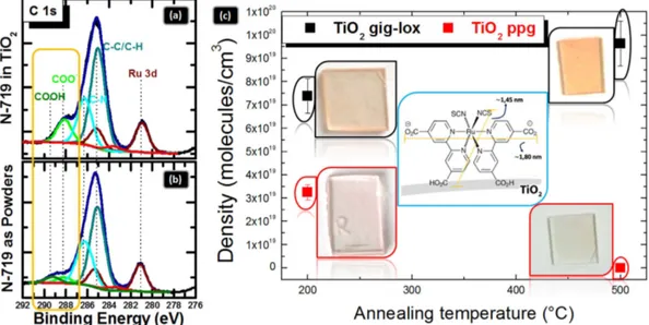
The empowering offered by the gig-lox structure was tested on its infiltration capability and sur-face reactivity by using test-molecules bearing a COOH group to be anchored on the TiO2 surfaces like N-7194,since largely used in the literature. X-Ray Photoelectron Spectroscopy was used to investigate the TiO2 surface
modification after sensitization (Fig. 7(a)). The band due to the C-C/C-H species is located at 285.0 eV, whilst the C-N bond and the COO− group give contributions at 286.3 eV and at 288.2 eV, respectively. As a fingerprint of
the anchoring, the last component is more pronounced in the gig-lox than in the powders spectrum (Fig. 7(b)). As a further evidence of the molecular anchoring on the TiO2 surface, the band at 289.4 eV, due to the unreacted Figure 4. Ellipsometric measurements. Spectroscopic Ellipsometric measurements of experimental (symbols)
and generated (lines) curves at 55° and 65° angles of incidence of Ψ (a), and of Δ (b) for the gig-lox layer as deposited; (c) transmission data (symbols) and simulated (lines) for gig-lox layer annealed at 500 °C and gig-lox layer annealed at 500 °C + N-719, (d,e) the calculated refractive index (n) and extinction coefficient (k) of ppg and gig-lox layers before and after annealing at 500 °C and for the gig-lox layer after annealing at 500 °C + N-719.
www.nature.com/scientificreports/
COOH groups, is not present in the spectrum of the infiltrated TiO2 layer. All those findings thus testify that dye
chemisorption is occurred on the TiO2 surface61. Chemisorption is the pre-requisite for photo-electron injection
from the dye to TiO2.
Spectroscopic Ellipsometry reveals the occurrence of some optical modifications after dye loading: an increase of the refractive index which was associated to the dye molecules filling the TiO2 pores (see Fig. 4(d) and Table 1);
a reduction of the layer transmittance in the range of 2.2–3.5 eV, wherein the specific absorption on N-719 is expected (Fig. 4(c)); and, accordingly, an increase of the extinction coefficient in the tail below 3.5 eV (Fig. 4(e)).
By UV-Vis absorption measurements we estimate the density D[N-719] using the Lambert-Beer law:
= ε × ×
‐
D[N 719] Ab NA, where A is the absorbance, ε is the molar absorption coefficient, b is the light path and the NA is the Avogadro’s number62. In our case, the molar absorption coefficient is ∼ 1.4 × 10⁴ M−1cm−1 4 (see Table
3S). The data were also represented in Fig. 7(c) as a function of the annealing temperature done before sensitiza-tion. From the comparison it emerges that the gig-lox layer annealed at 500 °C accommodates the largest amount of molecules, likely due to the crystallographic improvement of the surface exposed by the TiO2 rods edges with
respect to the starting material, comprising: a) the faceting of the external surfaces (see TEM in Fig. 5) and b) a likely increased reactivity of the anatase surfaces in comparison to less ordered surfaces3,4,25,63. Note that a value
of ∼ 1 × 10²⁰ molecules/cm3 is consistent with a complete pore filling as calculated by taking into account the full Figure 5. Structural analyses. (a) symmetric XRD patterns (2θ -ω ) of TiO2 layers deposited in gig-lox (red) and in ppg (blue) configuration after thermal treatment at 500 °C. Both patterns refer to anatase. TEM analyses of the TiO2 gig-lox layer after annealing at 500 °C: (b) bright field image showing the meso-porous structure (the
pores give a bright contrast); (c) dark field image originating from the region circled in (d), highlighting single grains stacked within the rods (the bright objects); (e) detail of a rod with the related SAED in (f). Left panel: a representative schematic of a TiO2 rod made of stacked grains with facets along (101) and (10-1) planes, with
growth axis along the [001] direction, according to XRD data in (a). The preservation of this fine structure denotes that the annealing has a conservative effect on the porosity.
www.nature.com/scientificreports/
volume of the pores and the N-719 size (the volume occupied by each molecule was ∼ 3.8 nm3). On the other
hand, a lower infiltration capability is offered by the ppg layer in the sample pre-treated at 200 °C due to the more
Figure 6. Representative schematic of gig-lox and ppg processes. The porosity of the gig-lox TiO2 layer is maintained even after annealing at 500 °C, while in the ppg TiO2 layer a dramatic pore shrinkage is observed
after the same thermal treatment. Note also: (1) the double plasma regime used in gig-lox; (2) the double range porosity (nano and meso) achieved in gig-lox.
Figure 7. Analyses on the dye loading process. XPS high resolution spectra in the C 1 s region for (a)
gig-lox TiO2 layer functionalized with N-719 compared to (b) N-719 powders. The comparison with the N-719
powders in (b) allows associating the contribution at 280.9 eV to the Ru 3d5/2 binding energy (the Ru 3d3/2
component is at 285.1 eV). The COO− groups, giving contributions 288.2 eV, are used as markers for the
molecular anchoring on the TiO2 surface; (c) density of molecules infiltrated into the differently pre-treated
TiO2 layers (gig-lox vs. ppg). Insets: photos of functionalized TiO2 glasses with the colour depending on the
www.nature.com/scientificreports/
compact overall structure (see Fig. 2d); moreover, grain coalescence definitively obstructs the dye infiltration in the sample pre-treated at 500 °C.
Devices.
As a first proof of concept, we employed the described gig-lox material in the architecture of Dye Sensitized Solar Cells. The photocurrent-voltage characteristics are shown in Fig. 8.They testify the successful combination of dye loading and chemisorption occurred into the TiO2 gig-lox
scaffold. Photo-conversion efficiencies of 6.3% were measured for the gig-lox layers (see methods for details), showing performances comparable to the commercial reference device. Those values are positively considered if taken in relationship to the reduced thickness of the scaffold (we used 1 μ m instead of ∼ 10 μ m as commonly done) and to the low molar absorption coefficient of the N-719 dye29,34. This represents our first demonstration
that a sputtered TiO2 layer aspires to compete with chemically prepared counterparts (integrated in the same
architecture), additionally offering the up-scalability of the growth process as added-value.
A second proof of concept was provided by integrating the TiO2 gig-lox layer as scaffold in Perovskite Solar
Cells, using a solution processed CH3NH3PbI3 material. Consistently with what already shown, a 1 μ m-thick
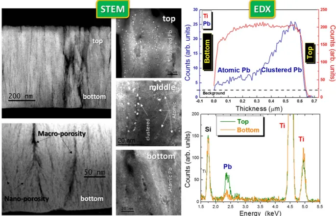
TiO2 layer was investigated and the extent of infiltration by the perovskite evaluated19,64,65. In Fig. 9 we
pro-vide the demonstration of the successful deep interpenetration between our gig-lox scaffold and the solution processed CH3NH3PbI3. Since STEM is very sensitive to species with high atomic number (Z), it indeed gives
evidence (mainly) of the spatial distribution of the Pb atoms. They are found to be atomically distributed through the layer or aggregated in nanometer spheres giving a bright contrast in the images. This results from (mainly) vacuum-induced degradation66,67 of the starting perovskite layer. Perovskite degradation occurs by creation and
loss of volatile species66, and this causes iodine leaving the sample likely in form of HI. The consequent huge
vol-ume contraction20 with respect to the initial perovskite distribution is responsible for the spatial discontinuity of
residual Pb species observed in Fig. 9. Nonetheless, the integral amount of Pb atoms, compared to the Ti counter-part (see EDX results in Fig. 9), accounts for a starting complete pore filling inside the TiO2 scaffold.
Although the information on the continuity of the perovskite coverage over the TiO2 rods is consequently lost,
the distribution and location of the Pb agglomerates depict the capability of the perovskite to deeply enter the structure (Pb distribution used as marker). As a matter of fact, in the STEM view of the top region of the sample, the Pb nano-agglomerates are vertically stacked into the TiO2 pores. A different scenario is encountered in the
bottom part of the layer wherein the Pb is atomically distributed (not aggregated) through the TiO2 layer even
entering into the nano-pores, as further supported by EDX profiling. The coexistence of atomic and clustered Pb is found in the middle part of the layer.
The results indeed indicate that the perovskite enters the TiO2 scaffold with a diffusion profile. This implies
that, scaling the gig-lox layer thickness to a value of 150–200 nm represents a strategy to get a uniform distri-bution of the infiltrated perovskite. This reduction of the layer thickness also positively combines with the high absorption coefficient offered by the perovskite materials18,68 (the dye, instead, having a relatively low absorption
coefficient, forces the TiO2 thickness to be more properly around 10 μ m to increase the density of light absorbers).
As a matter of fact, the penetration depth of light in CH3NH3PbI3 layers at 750 nm (close to the bandgap) is
∼ 250 nm: wavelengths shorter than that value have progressively smaller penetration depth.
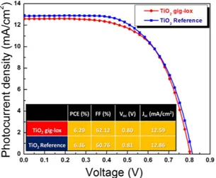
For device purposes, we were indeed authorized to scale the layer thickness to 150 nm. The related cell perfor-mances are shown in Fig. 10.
The solar cell based on gig-lox TiO2 exhibited a photoconversion efficiency of 11.7%. compared to a device
fabricated using commercially available colloidal TiO2 grains, which reached 10.5% efficiency. The curves do not
show hysteresis.
The enhanced photovoltaic performances of the gig-lox TiO2 are mainly ascribed to the higher photocurrent
density related to the fine grain morphology of the scaffold. In fact, the gig-lox TiO2 layer is characterized by
small interconnected grains, as seen in Figs 5 and 9. An additional value-added for the benefit of the device per-formances is given by the capillary pervasive infiltration of the perovskite into the multi-scale-pores of the gig-lox
Figure 8. I–V curves of DSCs. Devices (∼ 1 μ m-thick) based on gig-lox TiO2 layers compared to a reference made by commercial TiO2 pastes (Dyesol 18NR-T) under 1.0 sun illumination.
www.nature.com/scientificreports/
structure (Fig. 9); this leads to a more extended TiO2-perovskite interface that rises the electrons injection
effi-ciency. Although this value does not represent a record24, it states the potentialities of the material and encourages
further optimizations of the TiO2-perovskite blend and of the overall cell architecture.
Figure 9. STEM and EDX analyses on the TiO2 gig-lox layer after CH3NH3PbI3 infiltration. In the STEM
images, the Pb nano-aggregates (white Z-contrast) result from the perovskite degradation under high vacuum conditions66 and are used as markers of the original distribution of the perovskite layer. Notice how the Pb
aggregates nicely stack into the pores; also follow the Pb atomic distribution into the bottom part of the layer. Here the Pb/Ti atomic ratio is ∼ 1/10, close to what expected by combining their atomic density in the starting CH3NH3PbI3 (∼ 3Pb/1nm3) and in the TiO2 layer with the gig-lox porosity (CH3NH3PbI3/TiO2 ∼ 40% in
volume) in a regime of complete pore filling.
Figure 10. I–V curves of Perovskite Solar Cells. Devices based on gig-lox TiO2 layers (∼ 150 nm-thick) under 1.0 sun illumination (both are reverse curves).
www.nature.com/scientificreports/
Conclusions
We grow multi-porosity TiO2 scaffolds offering, in perspective, a transversal empowering over different
technolo-gies, including photovoltaics, sensors, water purification, water splitting etc. The method used is new, up-scalable, reliable and indeed industrially implementable, and can be, in principle, extended to any reactive metallic source to produce porous oxides. The multi-scale-porosity (nano and meso) represents the key parameter to allow mate-rial of different size (and nature) intimately entering into the TiO2 scaffold and forming an active interacting
(chemically and physically) blend such as with: dye molecules with their steric hindrance and their anchoring groups; hybrid perovskites with their own chemistry and nanostructuring. The material gains an average porosity of ∼ 40% in volume which is maintained up to (at least) 500 °C of post-deposition annealing; additionally, surface faceting represents an added-value for the TiO2 surface to interact with functional materials. In all those respects,
the gig-lox layer structure surpasses what achievable by sputtering in conventional ways. Its competition level with chemically synthesized reference counterparts is doubly demonstrated by integration of the gig-lox TiO2
scaffold in DSC and PSC architectures. A high photo-active molecular infiltration was proved by chemisorption of N-719 (∼ 1 × 10²⁰ molecules/cm3) on the TiO
2 surfaces. In Perovskite Solar Cells, the capillary infiltration of
CH3NH3PbI3 into the differently sized pores of the TiO2 architecture allowed reaching efficiency values of 11.7%,
higher than in the reference cell made with commercial TiO2 under the same conditions.
Materials and Methods
Sputtering equipment.
TiO2 layers have been deposited on corning glass slices by using two differentgeome-tries: a standard parallel plate geometry (Kenotec equipment–Magnetron DC-reactive sputtering) and a customized grazing incidence geometry (Kenosistec equipment–Magnetron DC-pulsed sputtering). The processes on both equipments were calibrated on the basis of the semi-empirical Thornton’s model (Tmelting anatase = 1843 °C)
with the intent of confining the TiO2 growth within the porous region (see Fig. 1(a)). Different parameters were
thus explored, namely: the anode-cathode distance, the flow rate of both the carrier gas (Ar) and reactive gas (O2), the power applied to the cathodes and the temperature on the substrate. The total pressure and the
depo-sition temperature were chosen as shown in Fig. 1(a), and the oxygen partial pressure was tuned in order to get stoichiometric TiO2 layers. In both working geometries, each deposition process is preceded by a pre-sputtering
step to clean up the surface of the Titanium target and to remove residual thin oxide layer. With our best process, mesoporous TiO2 layers were deposited at room temperature, with thickness in the range from 350 to 1000 nm.
The effect of post-deposition thermal treatments was also explored, namely at 200 °C for 30 minutes and at 500 °C for 30 (and also 450 °C 1 h) seconds both performed in a mixture of 78%N2:22%O2.
TiO
2deposition by grazing incidence geometry assisted by local oxidation (gig-lox).
We useda customized grazing incidence source of Titanium (2-inch circular target) at incident angle of 12.7° taken with respect to the sample surface. The choice of the incident angle was done on the basis of geometrical considera-tion, being a compromise between the deposition rate and the shadowing effectiveness. The other peculiarity of the equipment resides in the oxygen source location, being independent from the Ar source and placed in close proximity to the substrate. A schematic of the equipment is shown in Fig. 1(b). In our optimized process the Ar flow-rate was settled at 69 sccm, corresponding to a deposition pressure of 14.0 μ bar (10.5 mTorr-see working region inside the Thornton schematic of Fig. 1(a)). The depositions were done at room temperature in O2 reactive
ambient with a flow rate of 2 sccm, using a power of 140 W, a current of 475 mA and a voltage of 295 V (power loading 6.9 W/cm2). The corresponding growth rate was 4 nm/min, able to guarantee the proper layer
stoichi-ometry (as demonstrated by X-ray photoelectron spectroscopy analyses) by local oxidation during growth. The anode-cathode distance was set at 1.2 cm and, during deposition, the substrate was kept rotating under the beam (20 rpm) in order to improve the layer uniformity over the sample surface. In these working conditions, a dou-ble regime is settled up into the deposition chamber (see Fig. 1(b)): a blue plasma (metallic) in proximity of the source, and an oxidizing region confined at the sample surface (violet colour). This allowed avoiding charging effects and working under stable conditions, at relatively high deposition rate. As main focus, the procedure allows performing a progressive local oxidation during growth, thus avoiding ex-situ treatments in oxygen. The material used in the paper is the result of systematic action on the deposition parameters (see SI).
TiO
2deposition by parallel plate geometry (ppg).
We used a standard anode-cathode parallel plateequipment with a 6-inch circular target of Titanium as a source. The process was carried out in Oxygen ambient by applying a constant power of 600 W (1.24 A, 498 V, power loading 4.9 W/cm2). An O
2/Ar flow rate ratio as low
as of 5/45 sccm was set in order to maintain a growth rate comparable to that used in the gig-lox geometry (here 3.7 nm/min) and to guarantee the proper layer stoichiometry. The deposition processes were carried out at a pressure of 9.0 μ bar (7 mTorr-see working region inside the Thornton schematic of Fig. 1a) with an anode–cath-ode distance of 10 cm. In the chamber, a uniform plasma (pink colour), rich of oxygen species, was established between the plates.
Spectroscopic Ellipsometry analyses.
Spectroscopic Ellipsometry (SE) data were collected using aJ.A.Woollam VASE instrument. Measurements were performed in a vertical configuration, which is better suited for transparent samples in order to measure on the same point ellipsometric and transmittance data. Optical spectra were recorded from 300 to 2100 nm (step 5 nm) at 55°, 60° and 65°. An initial model of the optical transi-tions was built for each layer constituting the sample. The TiO2 layer was modeled by using a single Tauc-Lorentz
oscillator and the surface roughness by the Bruggeman effective medium approximation (EMA). We evaluated that the use of graded layer model by an increased number of fitting parameters easily leads to unphysical results. In order to fit the sample with absorbed N-719 dye in the spectral range from 2 eV to 3.25 eV, where the trans-mittance drops abruptly, we have used two additional Gaussian oscillators accounting for the N-719 absorption
www.nature.com/scientificreports/
bands centered at 2.33 eV and 3.15 eV. Special care has been taken to evaluate the optical constants for the glass substrate taking into account backside reflection and unpolarized light. Excellent data fitting has been obtained through the whole range of measurements (300–2100 nm) including transmittance data. From the fitting of the raw psi and delta data (Fig. 4(a,b)) we extracted the optical parameters n and k (the real and imaginary parts of the complex refractive index). The material porosity was measured using the same approach applied by Richards
et al.49, assuming that the nano-structuring (mainly grain size and stoichiometry) of the layer does not
remark-ably change with the annealing (as verified for the gig-lox layer). This allowed exploring the effect of the thermal treatment on the layer porosity.
Structural and morphological characterizations.
X-ray diffraction (XRD) analyses were performedby using a D8-Discover Bruker AXS diffractometer, equipped with a Cu Kα source, in symmetric
configura-tion (source and detector move by the same incremental angle). Transmission Electron Microscopy (TEM) and Selected Area Electron Diffraction analyses (SAED) were done using a JEOL JEM 2010 microscope operating at 200 kV. Field Emission Scanning Electron microscopy (FE-SEM) images were obtained by using a ZEISS VP 55 microscope equipped with Energy Dispersive X-ray analyses (EDX) INCA-Oxford windowless detector. STEM analysis are obtained using a Jeol ARM200 equipped with a cold FEG electron source, CEOS condenser aberra-tion corrector and 100 mm2 Jeol EDXS detector. Some images are acquired in STEM mode in Z-contrast
config-uration. EDXS profiles are extracted by a 730 × 180 nm spectrum image across the whole thickness, with 7 nm pixel size, and 0.1 s pixel time. The scanned area was selected in a thicker region of the sample in order to increase and average the signal.
Dye-sensitizing, XPS and UV-Vis characterization of the TiO
2layers.
The surface stoichiometry ofthe as deposited layers was investigated by X-Ray Photoelectron Spectroscopy (XPS). XPS analyses have been per-formed by using a PHI ESCA/SAM 5600 Multy technique spectrometer equipped with a Mg Kα X-ray source at a
pressure of 5 × 10⁻⁹ Torr. The TiO
2 layers were sensitized with di-tetrabutylammonium cis-bis (isothiocyanato)
bis (2,2-bipyridyl-4,4-dicarboxylato) ruthenium(II) (N-719, Aldrich) by immersion into 5 × 10⁻⁵ M Ethanol
solu-tions of the complex for 18 h at room temperature. The sensitized layers were withdrawn from the solution, rinsed in pure Ethanol to remove any physisorbed dye and dried in nitrogen flux. UV-VIS measurements were carried out on an UV-Vis V-650 JASCO spectrophotometer, and the spectra were recorded with a ± 0.2 nm resolution.
DSC architecture and I-V characterization.
Fluorine-doped tin oxide (FTO, 15 Ω/sq, provided bySolaronix S.A.) glass plates were first cleaned in a detergent solution using an ultrasonic bath for 15 min, and then rinsed with water and ethanol. Compact TiO2 layers were prepared as follows: FTO glasses were coated
with 0.15 M titanium diisopropoxide bis(acetylacetonate) (75% Aldrich) in 1-butanol (Aldrich) solution by the spin-coating method, which was heated at 125 °C for 5 min. After the coated film was cooled down to the room temperature, the same process was repeated and the two times coated FTO glasses were finally heated at 500 °C for 30 min. The prepared dense TiO2 blocking layer were thus covered by: 1) mesoporous TiO2 gig-lox layers
depos-ited by sputtering at RT; or 2) standard nanocrystalline TiO2 pastes (reference) deposited by a doctor-blading
technique using a commercial diluted colloidal titania paste (Dyesol 18NR-T). The reference samples were heated in air at 150 °C for 15 min. To compensate the limitations associated to the poor light harvesting capability29 of
the sensitizer and to reinforce the potentiality of the new material, we associated to the gig-lox scaffold to a com-mercial scattering layer by doctor blading a comcom-mercial scattering paste (Solaronix D/SP colloidal paste) onto the above described transparent layers and sintering the double-layer photoanode at 500 °C for 30 min. The same was done for the reference photoanode. For all the samples, the dye sensitization was performed by keeping the electrodes for 14 h and under dark in 0.2 mM solutions of bis(tetrabutylammonium)-cis-di(thiocyanato)-N,N′ -bis(4-carboxylato-4′ -carboxylic acid-2,2′ -bipyridine) ruthenium(II) (N-719, purchased by Solaronix S.A.) in a mixture of acetonitrile and tert-butyl alcohol (1:1 v/v). The counter-electrodes were prepared by sputtering a 50 nm Pt layer on a hole-drilled cleaned FTO plate. The photo-anode and the counter-electrode were faced and assembled using a suitably cut 50 μ m thick Surlyn
®
hot-melt gasket for sealing. The iodine redox electrolyte (0.1 M LiI, 0.03 M I2, 0.6 M 1-methyl-3-propylimidazolium iodide, and 0.5 M tert-butylpyridine in dry acetonitrile) wasvacuum-injected into the space between the electrodes through pre-drilled holes on the back of the counter elec-trode. The holes were eventually sealed using Surlyn
®
hot melt film and a cover glass. Photocurrent-voltage meas-urements were performed using a Keithley unit (Model 2400 Source Meter). A Newport AM 1.5 Solar Simulator (Model 91160 A equipped with a 1000 W Xenon arc lamp) serving as a light source.PSC architecture and I-V characterization.
Fluorine-doped tin oxide (FTO, 15 Ω/sq, provided bySolaronix S.A.) glass plates were first etched with zinc powder and HCl 2 M to form the desired electrode pattern, then cleaned in a detergent solution using an ultrasonic bath for 15 min, and rinsed with water and ethanol. A hole blocking layer of TiO2 (40 nm) was deposited on the cleaned FTO substrates by sputtering.
The TiO2 blocking layers were covered by: (1) mesoporous TiO2 gig-lox layers deposited by sputtering at RT;
or (2) standard nanocrystalline TiO2 pastes (reference) deposited by spin coating a commercial diluted colloidal
titania paste (Dyesol 30NR-T). The samples were heated in air at 450 °C for 1 h. The annealing is equivalent to 500 °C 30 s.
The perovskite films were deposited from a precursor solution containing 461 mg of PbI2, 159 mg of CH3NH3I,
and 78 mg of DMSO (molar ratio 1:1:1) in 600 mg of DMF. The completely dissolved solution was spin-coated on the TiO2 layer at 4000 rpm for 25 sec and 100 μ L of toluene were poured on the spinning substrate 15 s prior
to the end of the program. The film were heated at 65 °C for 1 min and 100 °C for 2 min in order to obtain a dense CH3NH3PbI3 film69. The hole transporting material solution, Spiro-MeOTAD, 50 mM in chlorobenzene
www.nature.com/scientificreports/
was spun at 3000 rpm for 30 s. As a last step, 60 nm of gold top electrode were thermally evaporated under high vacuum. Photocurrent-voltage measurements were performed using a Keithley unit (Model 2400 Source Meter). A Newport AM 1.5 Solar Simulator (Model 91160A equipped with a 1000W Xenon arc lamp) serving as a light source.
References
1. Liu, N. et al. Crystallographic Facet-Induced Toxicological Responses by Faceted Titanium Dioxide Nanocrystals. ACS Nano 10, 6062− 6073 (2016).
2. Zhai, P. et al. Trifunctional TiO2 Nanoparticles with Exposed {001} Facets as Additives in Cobalt-Based Porphyrin-Sensitized Solar
Cells. Adv. Funct. Mater. 25, 6093–6100 (2015).
3. Zhao, Z., Tian, J., Sang, Y., Cabot, A. & Liu, H. Structure, Synthesis, and Applications of TiO2 Nanobelts. Adv. Mater. 27, 2557–2582
(2015).
4. Grätzel, M. Solar Energy Conversion by Dye-Sensitized Photovoltaic Cells. Inorg. Chem. 44, 6841–6851 (2005).
5. Kojima, A., Teshima, K., Shirai, Y. & Miyasaka, T. Organometal Halide Perovskites as Visible-Light Sensitizers for Photovoltaic Cells.
J. Am. Chem. Soc. 131, 6050–6051 (2009).
6. Guo, W., Xue, X., Wang, S., Lin, C. & Wang, Z. L. An integrated power pack of dye-sensitized solar cell and Li battery based on double-sided TiO2 nanotube arrays. Nano Lett. 12, 2520–2523 (2012).
7. Cho, I. S. et al. Highly Efficient Solar Water Splitting from Transferred TiO2 Nanotube Arrays. Nano Lett. 15, 5709–5715 (2015).
8. Gao, H., Sun, M., Lin, C. & Wang, S. Electrochemical DNA Biosensor Based on Graphene and TiO2 Nanorods Composite Film for
the Detection of Transgenic Soybean Gene Sequence of MON89788. Electroanalysis 24, 2283–2290 (2012).
9. Karunagaran, B., Uthirakumar, P., Chung, S. J., Velumani, S. & Suh, E. K. TiO2 thin film gas sensor for monitoring ammonia. Materials Characterization 58, 680–684 (2007).
10. Li Wang, Y. et al. The gas sensing properties of TiO2 nanotubes synthesized by hydrothermal method. Chinese Chemical Letters 22,
603–606 (2011).
11. Fei, J. & Li, J. Controlled Preparation of Porous TiO2–Ag Nanostructures through Supramolecular Assembly for Plasmon-Enhanced
Photocatalysis. Adv. Mater. 27, 314–319 (2015).
12. Alberti, A. et al. Low temperature sputtered TiO2 nano sheaths on electrospun PES fibers as high porosity photoactive material. RSC Adv. 5, 73444–73450 (2015).
13. Yella, A. et al. Porphyrin-sensitized solar cells with cobalt (II/III)-based redox electrolyte exceed 12 percent efficiency. Science 334, 629–634 (2011).
14. Song, L. et al. Spray Deposition of Titania Films with Incorporated Crystalline Nanoparticles for All-Solid-State Dye-Sensitized Solar Cells Using P3HT. Adv. Funct. Mater. 26, 1498–1506 (2016).
15. O’Reagan, B. & Grätzel, M. A low-cost, high-efficiency solar cell based on dye-sensitized colloidal TiO2 films. Nature 353, 737-740
(1991).
16. Tian, H. et al. The Influence of Environmental Factors on DSSCs for BIPV. Int. J. Electrochem. Sci. 7, 4686–4691 (2012).
17. Mathew, S. et al. Dye-sensitized solar cells with 13% efficiency achieved through the molecular engineering of porphyrin sensitizers.
Nature Chemistry 6, 242–247 (2014).
18. Burschka, J. et al. Sequential deposition as a route to high-performance perovskite-sensitized solar cells. Nature 499, 316–319 (2013).
19. Miyasaka, T. Perovskite Photovoltaics: Rare Functions of Organo Lead Halide in Solar Cells and Optoelectronic Devices. Chem. Lett.
44, 720–729 (2015).
20. Alberti, A. et al. Similar Structural Dynamics for the Degradation of CH3NH3PbI3 in Air and in Vacuum. Chem. Phys. Chem. 16, 3064–3071 (2015).
21. Mahmood, K., Swain, B. S. & Amassian, A. Highly Efficient Hybrid Photovoltaics Based on Hyperbranched Three-Dimensional TiO2 Electron Transporting Materials. Adv. Mater. 27, 2859–2865 (2015).
22. Pascoe, A. R. et al. Enhancing the Optoelectronic Performance of Perovskite Solar Cells via a Textured CH3NH3PbI3 Morphology.
Adv. Funct. Mater. 26, 1278–1285 (2016).
23. Noh, J. H. & Seok, S. I. Steps toward efficient inorganic–organic hybrid perovskite solar cells. MRS Bulletin 40, 648–653 (2015). 24. Saliba, M. et al. Cesium-containing triple cation perovskite solar cells: improved stability, reproducibility and high efficiency. Energy
& Environ. Sci. 9, 1989–1997 (2016).
25. Pellegrino, G. et al. Study of the Anchoring Process of Tethered Unsymmetrical Zn-Phthalocyanines on TiO2 Nanostructured Thin
Films. J. Phys. Chem. C 117, 11176–11185 (2013).
26. Alberti, A. et al. Combined Strategy to Realize Efficient Photoelectrodes for Low Temperature Fabrication of Dye Solar Cells. ACS
Appl. Mater. Interfaces 6, 6425–6433 (2014).
27. Alberti, A. et al. Efficiency Enhancement in ZnO:Al-Based Dye-Sensitized Solar Cells Structured with Sputtered TiO2 Blocking
Layers. J. Phys. Chem. C 118, 6576–6585 (2014).
28. Liu, H., Avrutin, V., Izyumskaya, N., Özgür, Ü. & Morkoç, V. Transparent conducting oxides for electrode applications in light emitting and absorbing devices. Superlattices Microstruct. 48, 458–484 (2010).
29. Agosta, R. et al. An engineered co-sensitization system for highly efficient dye solar cells. Chem. Commun. 50, 9451–9453 (2014). 30. Miyasaka, T. Highlight Review: Perovskite Photovoltaics: Rare Functions of Organo Lead Halide in Solar Cells and Optoelectronic
Devices. Chem. Lett. 44, 720–729 (2015).
31. Alberti, A., Bongiorno, C. & Pellegrino, G. Anatase/Rutile nucleation and growth on (0002) and (11-20) oriented ZnO:Al/glass substrates at 150 °C. Thin Solid Films 555, 3–8 (2014).
32. Lin, J. J. et al. 3D Hierarchical Rutile TiO2 and Metal-free Organic Sensitizer Producing Dye-sensitized Solar Cells 8.6% Conversion
Efficiency. Sci. Rep. 4, 5769 (2014).
33. Lin, J. J. et al. Mesoporous anatase single crystals for efficient Co(2+ /3+ )-based dye-sensitized solar cells. Nano Energy 11, 557–567 (2015).
34. Lin, J. J. et al. N719- and D149-sensitized 3D hierarchical rutile TiO2 solar cells-a comparative study. Phys. Chem. Chem. Phys. 17,
7208–7213 (2015).
35. Thornton, J. A. The microstructure of sputter-deposited coatings. J. Vac. Sci. Technol. A 4, 3059–3065 (1986).
36. Movchan, B. A. & Demchishin, A. V. Study of the structure and properties of thick vacuum condensates of nickel, titanium, tungsten, aluminium oxide and zirconium dioxide. Phys. Met. Metallogr. 28, 83–90 (1969).
37. Kang, S. H. et al. Columnar rutile TiO2 based dye-sensitized solar cells by radio-frequency magnetron sputtering. Journal of Power Sources 184, 331–335 (2008).
38. Gomez, M. M., Lu, J., Olsson, E., Hagfeldt, A. & Granqvist, C. G. High efficiency dye-sensitized nanocrystalline solar cells based on sputter deposited Ti oxide films. Solar Energy Materials & Solar Cells 64, 385–392 (2000).
39. Gonzàlez-Garcìa, L., Gonzàlez-Valls, I., Lira-Cantu, M., Barranco, A. & Gonzàlez-Elipe, A. R. Aligned TiO2 nanocolumnar layers
prepared by PVD-GLAD for transparent dye sensitized solar cells. Energy & Enviromental Science 4, 3426–3435 (2011).
40. Zhou, Q., Li, Z., Ni, J. & Zhang, Z. A Simple Model to Describe the Rule of Glancing Angle Deposition. Materials Transactions 52, 469–473 (2011).
www.nature.com/scientificreports/
41. Li, Z., Teng, Y., Xing, L., Zhang, N. & Zhang, Z. Enhancement of the photocatalytic property of TiO2 columnar nanostructured films
by changing deposition angle. Materials Research Bulletin 50, 68–72 (2014).
42. Motemani, Y. et al. Adherence of human mesenchymal stem cells on Ti and TiO2 nano-columnar surfaces fabricated by glancing
angle sputter deposition. Applied Surface Science 292, 626–631 (2014).
43. Pihosh, Y. et al. Photocatalytic Properties of TiO2 Nanostructures Fabricated by Means of Glancing Angle Deposition and
Anodization. J. of the Electrochemical Society 156, K160–K165 (2009).
44. Chen, S., Li, Z. & Zhang, Z. Anisotropic TixSn1-xO2 nanostructures prepared by magnetron sputter deposition. Nanoscale Research Letters 6, 326–330 (2011).
45. Waits, R. K. Planar Magnetron Sputtering. J. Vac. Sci. Technol. 15, 179–187 (1978).
46. Gòmez, M. M. et al. Dye-sensitized sputtered titanium oxide films for photovoltaic applications: influence of the O2/Ar gas flow ratio during the deposition. Solar Energy Materials & Solar Cells 76, 37–56 (2003).
47. Sério, S., Melo Jorge, M. E., Maneira, M. J. P. & Nunes, Y. Influence of O2 partial pressure on the growth of nanostructured anatase phase TiO2 thin films prepared by DC reactive magnetron sputtering. Materials Chemistry and Physics 126, 73–81 (2011).
48. Lindgren, T. et al. Photoelectrochemical and optical properties of nitrogen doped titanium dioxide films prepared by reactive DC magnetron sputtering. J. Phys. Chem. B 107, 5709–5716 (2003).
49. Richards, B. S., Huong, N. T. P. & Crosky, A. Highly Porous Nanocluster TiO2 Films Deposited Using APCVD in an Excess of Water
Vapor. J. of The Electrochem. Soc. 152, F71–F74 (2005).
50. Zhang, H. & Banfield, J. F. Thermodynamic analysis of phase stability of nanocrystalline titania. J. Mater. Chem. 8, 2073–2076 (1998).
51. Park, T.-J., Levchenko, A. A., Zhou, H., Wong, S. S. & Navrotsky, A. Shape-dependent surface energetics of nanocrystalline TiO2. J. Mater. Chem. 20, 8639–8645 (2010).
52. Fukushima, K. & Yamada, I. Electrical properties of TiO2 films deposited by a reactive-ionized cluster beam. J. Appl. Phys. 65,
619–623 (1989).
53. Suhail, M. H., Mohan Rao, G. & Mohan & S. D. C. reactive magnetron sputtering of titanium-structural and optical characterization of TiO2 films. J. Appl. Phys. 71, 1421–1427 (1992).
54. Eufinger, K., Poelman, D., Poelman, H., De Gryse, R. & Marin, G. B. Effect of microstructure and crystallinity on the photocatalytic activity of TiO2 thin films deposited by dc magnetron sputtering. J. Phys. D: Appl. Phys. 40, 5232–5238 (2007).
55. Karunagaran, B., Rajendra Kumar, R. T., Mangalaraj, D., Narayandass, Sa. K. & Mohan Rao, G. Influence of thermal annealing on the composition and structural parameters of DC magnetron sputtered titanium dioxide thin films. Cryst. Res. Technol. 37, 1285–1292 (2002).
56. Meng, L.-J., Andritschky, M. & dos Santos, M. P. The effect of substrate temperature on the properties of d.c. reactive magnetron sputtered titanium oxide films. Thin Solid Films 223, 242–247 (1993).
57. Schiller, S., Beister, G. & Sieber, W. Influence of deposition parameters on the optical and structural properties of TiO2 films
produced by reactive d.c. plasmatron sputtering. Thin Solid Films 83, 239–245 (1981).
58. Pagliaro, M., Palmisano, G., Ciriminna, R. & Loddo, V. Nanochemistry aspects of titania in dye-sensitized solar cells. Energy &
Environ. Sci. 2, 838–844 (2009).
59. Buonsanti, R. et al. Hyperbranched Anatase TiO2 Nanocrystals: Nonaqueous Synthesis, Growth Mechanism and Exploitation in
Dye-Sensitized Solar Cells. J. Am. Chem. Soc. 133, 19216–19239 (2011).
60. Hanaor, C. & Sorrell, C. Review of the anatase to rutile phase transformation. J. Mater Sci. 46, 855–874 (2011).
61. Singh, J. et al. XPS, UV–vis, FTIR, and EXAFS studies to investigate the binding mechanism of N719 dye onto oxalic acid treated TiO2 and its implication on photovoltaic properties. J. Phys. Chem. C 117, 21096–21104 (2013).
62. Li, D., Swanson, B. I., Robinson, J. M. & Hoffbauer, M. Porphyrin Based Self-Assembled Monolayer Thin Films: Synthesis and Characterization. J. Am. Chem. Soc. 115, 6975–6980 (1993).
63. Pellegrino, G. et al. Dye-Sensitizing of Self-Nanostructured Ti(:Zn)O2/AZO Transparent Electrodes by Self-Assembly of
5,10,15,20-Tetrakis(4 carboxyphenyl)porphyrin. J. Phys. Chem. C 115, 7760–7767 (2011).
64. Pellegrino, G. et al. A. Texture of MAPbI3 Layers Assisted by Chloride on Flat TiO2 Substrates. J. Phys. Chem. C 119, 19808–19816
(2015).
65. Colella, S. et al. Elusive Presence of Chloride in Mixed Halide Perovskite Solar Cells, J. Phys. Chem. Lett. 5, 3532–3538 (2014). 66. Smecca, E. Stability of solution-processed MAPbI3 and FAPbI3 layers. Phys. Chem. Chem. Phys. 18, 13413–13422 (2016). 67. Deretzis, I. et al. Atomistic origins of CH3NH3PbI3 degradation to PbI2 in vacuum. Appl. Phys. Lett. 106, 131904–4 (2015). 68. Leguy, A. M. A. et al. Experimental and theoretical optical properties of methylammonium lead halide perovskites. Nanoscale 8,
6317–6327 (2016).
69. Ahn, N. et al. Highly Reproducible Perovskite Solar Cells with Average Efficiency of 18.3% and Best Efficiency of 19.7% Fabricated via Lewis Base Adduct of Lead(II) Iodide. J. Am. Chem. Soc. 137, 8696–8699 (2015).
Acknowledgements
The authors thank Stefano Perugini, Giovanni Barbieri and Carlo Aliberti (Kenosistec S.r.l.) for the technical collaboration and assistance on the customization of sputtering equipments. This work was partially supported by the Italian Project “Elettronica su Plastica per Sistemi Smart disposable” (Electronics on Plastics for ‘Smart disposable’ Systems) funded by MIUR (Ministero Istruzione Università e Ricerca) to the Distretto Tecnologico Sicilia Micro e Nano Sistemi by means of the Italian Program PON02_00355_3416798.
Author Contributions
A.A. conceived the new deposition method and designed the experiments; with the support of A. La M., she made coordination actions and wrote the manuscript. S.S.: performed the deposition of all the materials discussed in the paper and dealt with most of the data analyses. XRD measurements were done by E.S.: G.M. performed Spectroscopic Ellipsometry and Transmission measurements accompanied by data modelling. C.B. performed TEM analyses. G.P. and G.G.C. performed surface HR-XPS and UV-VIS analyses. M.R.C. performed SEM analyses. R.I. and L. De M. realised and characterised the solar cells. G.M., F.N. i and C.S. critically revised the manuscript and contributed to data interpretation.
Additional Information
Supplementary information accompanies this paper at http://www.nature.com/srep Competing financial interests: The authors declare no competing financial interests.
www.nature.com/scientificreports/
How to cite this article: Sanzaro, S. et al. Multi-Scale-Porosity TiO2 scaffolds grown by innovative sputtering methods for high throughput hybrid photovoltaics. Sci. Rep. 6, 39509; doi: 10.1038/srep39509 (2016).
Publisher's note: Springer Nature remains neutral with regard to jurisdictional claims in published maps and
institutional affiliations.
This work is licensed under a Creative Commons Attribution 4.0 International License. The images or other third party material in this article are included in the article’s Creative Commons license, unless indicated otherwise in the credit line; if the material is not included under the Creative Commons license, users will need to obtain permission from the license holder to reproduce the material. To view a copy of this license, visit http://creativecommons.org/licenses/by/4.0/