FACOLTÁ DI INGEGNERIA
DIPARTIMENTO DI INGEGNERIA ELETTRICA ELETTRONICA ED INFORMATICA
DOCTOR OF PHILOSOPHY IN ELECTRONIC, AUTOMATION AND CONTROL OF COMPLEX
SYSTEMS ENGINEERING XXV Cycle
G
IORGIOM
AIELLAROA
NALOG AND
D
IGITAL
C
IRCUITS IN A
C
OMPLEMENTARY
O
RGANIC
TFT
T
ECHNOLOGY ON
F
LEXIBLE
S
UBSTRATE
P
H.D. T
HESIS TUTOR: PROF.G.PALMISANO COORDINATOR: PROF.L.FORTUNA 2011 - 2012I
Acknowledgment
I would like to thank my advisor, Prof. Giuseppe Palmisano, for guiding and supporting me during these years and for giving me the chance to work in a challenging research environment. I would also like to thank Eng. Egidio Ragonese and Eng. Francesco Carrara for their valuable technical advice and cooperation. I am very grateful to my friend and colleague Alessandro Castorina, his technical support was crucial to achieving good experimental results. I would also like to thank my colleagues at RF-ADC and STMicroelectronics Catania, each of them has contributed in some way to my personal and professional growth.
Last but not least, I would like to express my deeply gratitude to my parents and my brother; they have always believed in me. This thesis work is dedicated to them.
III
Publications
[1] M. Rapisarda, A. Valletta, G. Fortunato, L. Mariucci, M. Benwadih, S. Jacob, R. Coppard, F. Tramontana, L. Maddiona, A. Scuderi, G. Maiellaro, and F. Carrara, “Modeling of the electrical characteristics of fully printed CMOS Organic Thin Film Transistors including contact effects” Proceedings of the International Conference on
Organic Electronics 2011, June 22-24, 2011, CNR,
Rome, Italy.
[2] S. Abdinia, F. Torricelli, M. Benwahid, R. Coppard, A. Daami, S. Jacob, L. Maddiona, G. Maiellaro, L. Mariucci, M. Rizzo, F. Tramontana, A.H.M. van Roermund, and E. Cantatore, “Design of digital and analogue building blocks based on Monte Carlo simulations for a fully printed organic complementary technology,” Proceedings of the International Conference
on Organic Electronics 2012, Terragona, Spain June
25-27, 2012
[3] S. Jacob, M. Benwadih, J. Bablet, I. Chartier, R. Gwoziecki, S. Abdinia, E. Cantatore, L. Maddiona,
IV
F. Tramontana, G. Maiellaro, L. Mariucci, G. Palmisano, R. Coppard, “High performance printed N and P-type OTFTs for complementary circuits on plastic substrate,”
Proceedings of the European Solid-State Device Conference (ESSDERC), 17–21 Sept. 2012, pp. 173–176.
[4] S. Abdinia, M. Benwadih, E. Cantatore, I. Chartier, S. Jacob, L. Maddiona, G. Maiellaro, L. Mariucci, G. Palmisano, M. Rapisarda, F. Tramontana, A. H. M. van Roermund, “Design of analog and digital building blocks in a fully printed complementary organic technology,” Proceedings of the European Solid-State
Device Conference (ESSCIRC), 17–21 Sept. 2012,
pp. 145–148.
[5] S. Abdinia, R. Coppard, S. Jacob, G. Palmisano, G. Maiellaro, M. Rizzo, A. Scuderi, F. Tramontana, A. H. M. van Roermund and E. Cantatore, “A 4-bit ADC Manufactured in a Fully-printed Organic Complementary Technology Including Resistors” Accepted to International Solid-State Circuits Conference (ISSCC) 2013.
V
Table of Contents
Chapter 1
1.1 Introduction ... 1 1.2 Research background ... 5 1.3 Key applications ... 81.3.1 Low-end smart cards and electronics identification tags ... 9
1.3.2 Sensors ... 11
1.3.3 Flat panel displays ... 12
1.4 Objectives of research activity ... 14
Chapter 2
2.1 Organic thin film transistor ... 212.1.1 Organic TFT operation ... 24
2.1.2 Electrical characteristic of organic TFT... 28
2.1.3 Organic TFT structures ... 33
2.1.3.1 Bottom Gate – Bottom Contact ... 33
2.1.3.2 Bottom Gate – Top Contact ... 34
2.1.3.3 Top Gate – Top Contact ... 35
VI
2.2 Fully-printed organic complementary technology on
flexible substrate ... 38
2.3 Digital and analog basic building blocks ... 46
2.3.1 Static CMOS inverter and NAND gate ... 46
2.3.2 7-stage CMOS ring oscillator ... 56
2.3.3 Static CMOS J/K flip-flop ... 61
2.3.4 Dynamic CMOS NAND gate and positive edge triggered TSPC D flip-flop ... 66
2.3.5 Single-stage CMOS differential amplifier with active load ... 77
2.3.6 Rectifier and envelope detector ... 82
2.3.6.1 Description ... 82
2.3.6.2 Measurement results ... 83
Chapter 3
3.1 Introduction ... 933.2 Single-stage folded-cascode amplifier ... 93
3.2.1 Description ... 93
3.2.2 Measurement results ... 98
3.3 Cascode stacked-mirror and 2-stage high-gain OTAs .. 104
3.3.1 Description ... 104
3.3.2 Measurement results ... 108
3.4 Switched-capacitor comparator... 120
VII
3.4.2 Measurement results ... 125
Chapter 4
4.1 Organic light sensor ... 1294.1.1 Description ... 129
4.1.2 Measurement results ... 141
4.1.2.1 Organic photodiode ... 141
4.1.2.2 Operational amplifier ... 145
IX
List of Figures
Chapter 1
Fig. 1.1. Flexible RFID tag fabricated by PolyIC ... 10 Fig. 1.2. 55-inch flexible OLED display developed by LG
Electronics ... 13
Chapter 2
Fig. 2.1. Historic progress in the performance and maximum
reported carrier mobility of organic TFTs ... 22
Fig. 2.2. Schematic cross-section of OTFT ... 24 Fig. 2.3. OTFT in accumulation regime; total drain-source
current is the sum of channel current and bulk current ... 26
Fig. 2.4. OTFT in transition regime; bulk current represents
the main contribution to the total drain-source current ... 26
Fig. 2.5. OTFT in depletion regime; the drain-source current
typically decreases by increasing the gate-source voltage ... 27
Fig. 2.6. Output characteristics of a p-type OTFT ... 29 Fig. 2.7. Square-root of IDS current versus VGS voltage for a
X
Fig. 2.8. Transfer characteristics of a p-type OTFT on
logarithmic scale ... 32
Fig. 2.9. Bottom Gate–Bottom Contact structure (BG–BC) . 34 Fig. 2.10. Bottom Gate–Top Contact structure (BG–TC) ... 35 Fig. 2.11. Top Gate–Top Contact structure (TG–TC) ... 36 Fig. 2.12. Top Gate–Bottom Contact structure (TG–BC) ... 37 Fig. 2.13. Picture of 11 cm x 11 cm flexible foil with fully
printed OTFTs and digital and analog CMOS basic building blocks ... 39
Fig. 2.14. Transistor cross-section of the fully-printed organic
complementary technology on flexible substrate developed by CEA ... 40
Fig. 2.15. Microphotograph of a multi-finger OTFT with a
W = 2000 µm and L = 20 µm fabricated by CEA ... 40
Fig. 2.16. Schematic view of the fabrication process steps of
the fully-printed complementary organic technology on flexible substrate developed by CEA ... 42
Fig. 2.17. Output characteristic of p-type OTFT with channel
width and length of 2000 µm and 20 µm, respectively ... 44
Fig. 2.18. Transfer characteristic of p-type OTFT with
channel width and length of 2000 µm and 20 µm, respectively
... 44
Fig. 2.19. Output characteristic of n-type OTFT with channel
width and length of 2000 µm and 20 µm, respectively ... 45
Fig. 2.20. Transfer characteristic of n-type OTFT with
channel width and length of 2000 µm and 20 µm, respectively
XI
Fig. 2.21. Symbol, truth table and schematic of a static CMOS
inverter ... 47
Fig. 2.22. Layout picture and photograph of the static CMOS
inverters ... 49
Fig. 2.23. Input-output characteristics of the three inverters at
two different supply voltages ... 50
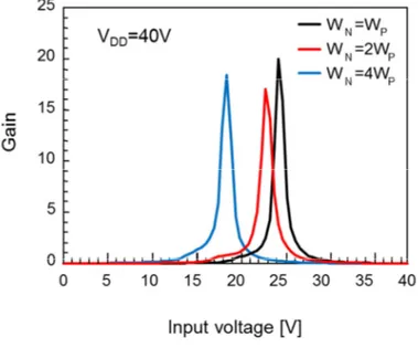
Fig. 2.24. Gain vs. input voltage of the three CMOS inverters
for a supply voltage of 40 V ... 52
Fig. 2.25. Symbol, truth table and schematic of a static CMOS
NAND gate ... 53
Fig. 2.26. Layout picture and photograph of the static CMOS
NAND gate ... 54
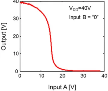
Fig. 2.27. Measured dc characteristic of the static CMOS
NAND gate ... 55
Fig. 2.28. Schematic of the 7-stage CMOS ring oscillator ... 57 Fig. 2.29. Layout picture of the 7-stage CMOS ring oscillator
... 58
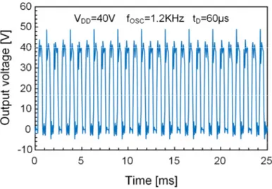
Fig. 2.30. Photograph of the 7-stage CMOS ring oscillator 58 Fig. 2.31. Output waveform of the 7-stage CMOS ring
oscillator at a supply voltage of 40 V ... 59
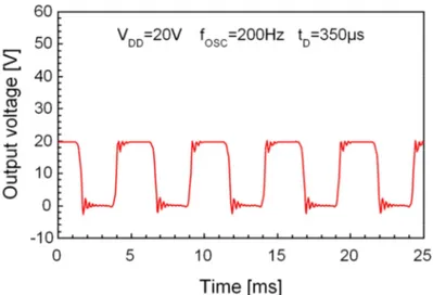
Fig. 2.32. Output waveform of the 7-stage CMOS ring
oscillator at a supply voltage of 20 V ... 60
Fig. 2.33. Symbol and truth table of a static CMOS J/K
flip-flop ... 61
Fig. 2.34. Schematic of a static CMOS J/K flip-flop
XII
Fig. 2.35. Schematic of three and two inputs static CMOS
NAND gates used for designing the static CMOS J/K flip-flop
... 63
Fig. 2.36. Layout picture of the static CMOS J/K flip-flop ... 64 Fig. 2.37. Photograph of the static CMOS J/K flip-flop ... 64 Fig. 2.38. Experimental result of the static CMOS J/K
flip-flop ... 65
Fig. 2.39. Basic structure of a dynamic logic gate
implemented with PDN ... 68
Fig. 2.40. Schematic of the dynamic CMOS NAND gate with
an additional static CMOS output buffer ... 69
Fig. 2.41. Layout picture and photograph of the dynamic
CMOS NAND gate with static CMOS output buffer ... 70
Fig. 2.42. Experimental result of the dynamic NAND gate for
two different input states (A = ”0”, B = ”1” and A = ”1”, B = ”1”) ... 72
Fig. 2.43. Schematic of the positive edge triggered TSPC D
flip-flop ... 73
Fig. 2.44. Layout picture of the positive edge triggered TSPC
D flip-flop ... 74
Fig. 2.45. Photograph of the positive edge triggered TSPC D
flip-flop ... 75
Fig. 2.46. Experimental result of the positive edge triggered
TSPC D flip-flop ... 76
Fig. 2.47. Schematic of the single stage CMOS differential
amplifier with complementary active load. (a) n-type input differential pair; (b) p-type input differential pair ... 77
XIII
Fig. 2.48. Layout picture and photograph of the p-type
differential amplifier with current mirror active load ... 79
Fig. 2.49. Short-circuit output current of the single stage
n-type differential amplifier with current mirror active load ... 80
Fig. 2.50. Short-circuit output current of the single stage
p-type differential amplifier with current mirror active load ... 81
Fig. 2.51. Measurement setup of the rectifier/envelope
detector ... 84
Fig. 2.52. Rectifier output voltage as a function of input
frequency at different load currents ... 84
Fig. 2.53. Rectifier output voltage as a function of load
current at 13.56-MHz input frequency ... 85
Fig. 2.54. Rectifier output voltage as a function of input signal
amplitudes for different input frequencies ... 86
Fig. 2.55. Diode dc characteristics before and after
large-signal ac measurements ... 87
Chapter 3
Fig. 3.1. Schematic of the single-stage folded-cascode
transconductance amplifier ... 94
Fig. 3.2. Layout picture of the single-stage folded-cascode
transconductance amplifier ... 97
Fig. 3.3. Photograph of the single-stage folded-cascode
XIV
Fig. 3.4. Measured input-output dc characteristic and
short-circuit output current of the single-stage folded-cascode amplifier ... 99
Fig. 3.5. Measurement setup for open-loop gain
characterization ... 100
Fig. 3.6. Measured open-loop gain and phase of the
single-stage folded-cascode amplifier ... 101
Fig. 3.7. Measured closed-loop gain in inverting
configuration of the folded-cascode amplifier ... 102
Fig. 3.8. Measured THD of the single-stage folded-cascode
amplifier ... 103
Fig. 3.9. Schematic of the cascode stacked-mirror OTA .... 105 Fig. 3.10. Schematic of the 2-stage OTA ... 106 Fig. 3.11. Layout picture and photograph of the cascode
stacked-mirror OTA ... 107
Fig. 3.12. Layout picture and photograph of the 2-stage OTA
... 108
Fig. 3.13. Input-output characteristic and short-circuit output
current of the cascode stacked-mirror OTA ... 109
Fig. 3.14. Input-output characteristic and short-circuit output
current of the 2-stage OTA ... 110
Fig. 3.15. Measurement setup for open-loop gain
characterization of the cascode stacked-mirror OTA ... 111
Fig. 3.16. Measurement setup for step-response
XV
Fig. 3.17. Measured open-loop gain and phase of the cascode
stacked-mirror OTA ... 113
Fig. 3.18. Measured step-response of the cascode stacked-mirror OTA ... 114
Fig. 3.19. Measurement setup for step-response characterization of the 2-stage OTA ... 115
Fig. 3.20. Measured step-response of the 2-stage OTA ... 116
Fig. 3.21. Measured closed-loop gain of both OTAs in inverting closed-loop configuration ... 117
Fig. 3.22. Measured THD at 2 Hz in inverting configuration of both OTAs ... 118
Fig. 3.23. Simplified schematic of the SC comparator ... 120
Fig. 3.24. Detailed schematic of the SC comparator ... 121
Fig. 3.25. Control signals of the SC comparator ... 121
Fig. 3.26. Layout picture and photograph of the switched-capacitor comparator ... 124
Fig. 3.27. Switched-capacitor comparator measurement for an input signal frequency of 20 Hz and a sampling frequency of 120 Hz ... 125
Chapter 4
Fig. 4.1. Circuit schematic of the organic light sensor ... 129Fig. 4.2. Schematic of the 2-stage OTA ... 130
Fig. 4.3. Circuit schematic of the light sensor with the OPD equivalent circuit ... 133
XVI
Fig. 4.4. Cross-section and layout bottom view of the
encapsulated organic photodiode ... 135
Fig. 4.5. Layout picture of the stand-alone OP-AMP ... 136 Fig. 4.6. Layout pictures of the foil-to-foil organic light
sensor ... 137
Fig. 4.7. Layout picture of the on-foil light sensor with
integrated nominal passive components ... 139
Fig. 4.8. Layout picture of the on-foil light sensor with
integrated reconfigurable passive components ... 140
Fig. 4.9. Photograph of the organic photodiode fabricated on
flexible plastic substrate ... 141
Fig. 4.10. I-V characteristics of the OPD measured at
different intensity of incident light ... 142
Fig. 4.11. I-V characteristics of the OPD measured at
different intensity of incident light after 12 hours from the first measurement ... 143
Fig. 4.12. The first and the second (after 12 hours) measured
I-V characteristic of the OPD in dark and maximum
illumination condition, respectively ... 144
Fig. 4.13. Photograph of the measurement setup adopted for
the characterization of the operational amplifier ... 145
Fig. 4.14. Detailed photograph of the PCB and the
operational amplifier glued on flexible flat cable ... 146
Fig. 4.15. Input-output characteristic of the operational
amplifier at three different supply voltages ... 147
Fig. 4.16. dc open-loop gain vs. input voltage of the
XVII
Fig. 4.17. Output short-circuit current vs. input voltage of the
operational amplifier at three different supply voltages ... 149
Fig. 4.18. Measurement setup adopted for step-response
characterization of the operational amplifier in closed-loop configuration ... 150
Fig. 4.19. Measured step-response of the operational
amplifier in closed-loop configuration (i.e. light sensor configuration) ... 151
Fig. 4.20. Measurement setup adopted for current step
response characterization of the operational amplifier in closed-loop configuration ... 152
Fig. 4.21. Measured output voltage of the operational
amplifier in closed-loop configuration when a discrete current ramp is applied at the input ... 153
Fig. 4.22. Photograph of the measurement setup adopted for
the foil-to-foil light sensor characterization ... 154
Fig. 4.23. Photograph of the foil-to-foil light sensor ... 155 Fig. 4.24. Measurement setup adopted for the light sensor
characterization ... 156
Fig. 4.25. Foil-to-foil light sensor output voltage variation
measured at ten different values of the incident light intensity
XIX
List of Tables
Chapter 2
Table 2.1. Main parameters of the complementary organic
TFTs reported in [9] (2005) and [10] (2012), respectively .. 23
Table 2.2. Measured electrical characteristics of both p-type
and n-type OTFT with W=2000 µm and L=2000 µm ... 43
Table 2.3. Transistor sizing of the static CMOS inverters ... 48 Table 2.4. Transistor sizing of the static CMOS NAND gate 54 Table 2.5. Transistor sizing of the 7-stage CMOS ring
oscillator ... 57
Table 2.6. Transistor sizing of the static CMOS J/K flip-flop
... 63
Table 2.7. Transistor sizing of the dynamic CMOS NAND
gate and static CMOS output buffer ... 70
Table 2.8. Transistor sizing of the positive edge triggered
TSPC D flip-flop ... 74
Table 2.9. Transistor sizing of both n-type and p-type single
XX
Chapter 3
Table 3.1. Transistor sizing and parasitic capacitances of the
single-stage folded-cascode transconductance amplifier ... 96
Table 3.2. Transistor sizing and parasitic capacitances of the
cascode stacked-mirror OTA ... 105
Table 3.3. Transistor sizing and parasitic capacitances of the
2-stage OTA ... 106
Table 3.4. Summary of the measured performance ... 119 Table 3.5. Transistor sizing and parasitic capacitances of the
SC comparator ... 122
Chapter 4
Table 4.1. Transistor sizing and parasitic capacitances of the
OP-AMP designed for the integration of organic light sensor
... 132
Table 4.2. Summary of the simulated performance of the
OP-AMP and light sensor, respectively... 134
Table 4.3. Range of variation of each reconfigurable passive
component ... 139
Table 4.4. Measured OPD current in dark and maximum
illumination condition at two different reverse bias voltages
XXI
Abstract
During the last decades, organic semiconductor technology on flexible substrate is attracting the interest of both academia and industrial communities since it is considered a very promising alternative to silicon technology in those applications where low cost, flexibility, and capability to cover large surfaces are required. The great advantage of organic thin-film transistor (OTFT) technology is the direct fabrication of circuits on low-cost plastic foils by using both low processing temperatures and printing methods that guarantee cost-efficient production. Several applications were faced by using OTFTs, such as flexible displays, RFID tags and organic processors. Such technologies also allow the integration on the same substrate of different kinds of organic sensors (i.e., light, temperature, pressure, humidity, pH, biosensors, etc.) in order to implement fully-integrated flexible organic smart sensors.
Despite these interesting developments, most OTFT processes still feature only p-type transistors, while very few complementary OTFT (C-OTFT) platforms have been
XXII
developed. Of course, the availability of a reliable process flow featuring both p-type and n-type transistors is now of utmost importance to advance in industrial applications development. Indeed, complementary organic technology would allow the implementation of complex digital circuits with higher yield and lower current consumption, as well as an increased reliability in mixed analog/digital circuits.
Research efforts on organic electronics have been mainly addressed towards digital circuits, while there is still a serious lack of significant results in the analog field. This lacuna hampers the advance towards the implementation of fully-integrated mixed-signal organic systems, including analog front-ends, signal conditioning, and/or analog-to-digital conversion (i.e., RFIDs, smart sensors, etc.).
In this thesis work analog and digital basic building blocks (i.e., inverters, static and dynamic logic gates, static and dynamic flip-flops, ring oscillator, differential gain stage, and rectifier/envelope detector) fabricated using a fully-printed organic complementary technology on flexible substrate are presented. The performance of the rectifier/envelope detector are explored up to 13.56-MHz thus demonstrating that adopted technology is suitable for the implementation of a flexible organic RFID tag.
XXIII
Moreover, design of complex analog building blocks (i.e. folded-cascode transconductance amplifier, 2-stage OTA, stacked-mirror OTA and switched-capacitor comparator) are also faced since the research on complementary organic analog circuits is still at very beginning and they are essential for enabling the implementation of fully-integrated mixed-signal systems (i.e., smart sensor interfaces, wireless communication systems, etc.). The measured performance of the single-stage folded-cascode transconductance amplifier is the best-in-class for complementary OTFT technologies on flexible substrate.
Finally, design and experimental results of the first fully-integrated flexible organic light sensor are also presented.
1
Chapter 1
1.1 Introduction
Organic electronics is an emerging technology field that is attracting the interest of both academia and industrial communities. Recent advances in organic electronics open new perspectives on developing much cheaper technologies for manufacturing electronic circuits and systems. Key to these new developments is the performance of organic thin-film transistors. Organic technology cannot achieve the performance of the silicon-based technologies in a relatively short time but it is expected to become suitable for designing complex electronic circuits and systems. Many researchers and companies are focused on development of new technologies, circuits and complex systems based on organic materials.
Organic semiconductor technology is expected to be able to create innovative applications and it is considered to be a new class of electronics with a huge market potential.
The processing characteristics and performance of FOLAE (Flexible Organic Large-Area Electronics) technology so far
2
show that it can be used for exiting or novel applications requiring large-area coverage, flexibility, and low temperature processing and low manufacturing cost. Moreover, large-area organic electronics will become “invisible”. Thanks to all these characteristics the new products could be integrated in most of daily live consumer goods, such us clothing, cars, houses, packaging and many others.
According to a study conducted by the US marketing research institute IDTechEx in 2006, the global market for organic and printed electronics will grow from its current 1.18 billion US dollars to more than 40 times that, to a volume of 48.18 billion US dollars, within the next 10 years [1].
A long-term market evaluation is difficult to do for an emerging technology but this preliminary forecast of the market share clearly indicates a strongly positive trend for FOLAE technology, in particular for logic and memory segment.
The logic segment covers all the applications of electronic circuits made on flexible substrate by printing or printing like processes. The segment named “Plastic Electronics” includes high-volume markets such as: large-area sensing applications, Radio Frequency IDentification and intelligent tags, electronics circuits for entertainment and games.
3
The ability to integrate on the same organic substrate all the functionalities needed to realize a complex system is the differentiating advantage of flexible organic and large area electronics that will create new applications and markets. In the last decade several basic functionalities, such as backplane matrices, displays, light emission and detection, sensing, energy storage and circuits for RF-ID, etc., have been realized. However, electronic circuits needed to integrate complete systems are so complex that a hybrid implementation with silicon-based technologies is still required.
A first revolution in the flexible organic large area electronic field was brought around 2006 by the chemical companies which have developed and commercialized air stable p-type organic semiconductors. Based on these materials, mature technologies are suitable for display backplane matrices and to drive a specific actuator for example in flexible Braille displays [2].
Except for these specific applications, p-type only circuits show strong limitations in performance: intrinsic high operating voltages and low switching speeds; low noise margin and sensitivity to variability, hence low yield and no possibility to build circuits with complex functionality. These major drawbacks of p-type only circuits limit the possible
4
applications of organic large area electronics to low complexity digital circuits.
A new revolution for the organic technology is needed in order to make the ambitious market forecast became a reality. The complementary organic technology, also named “organic CMOS technology” is the key point for developing all applications that nowadays the p-type only technology does not permit. Indeed, organic CMOS technology will allow to reach higher complexity digital circuits with substantial high yield and at low operating voltage and will also allow the integration of analogue circuits that are required to address many of the potential electronics applications like sensors, actuators and radio frequency communication systems.
In the recent years, chemical companies such as POLYERA, BASF and many others, brought to the market the first generation of n-type organic semiconductors that are printable and air-stable, enabling the development of the complementary organic technology.
Scientific community must, however, still overcome huge technical challenges in order to develop a stable and reliable organic CMOS technology that could be transferred to industry environment and enable the new applications.
5
1.2 Research background
Organic TFTs have seen a large research and development effort in the past ten years as they can be processed at ambient temperature, starting from the soluble, ink-like materials. The reduced temperature budget and the thin-film approach enable:
- To manufacture electronics on basically any substrate, for instance flexible plastic films, making it possible to integrate electronics on cheap flexible surfaces.
- To cover large surfaces with electronics at an extremely low cost per unit area using simple and high throughput technologies like printing.
Research on organic electronics by many industrial and academic research groups focused on application like flexible displays [3], low cost identification tags or RF-ID tags [4], photovoltaic surfaces and cells [5], sensors [6], etc. Some of these efforts are now leading to real product, like roll-up displays (Polymer Vision) [7] and low-end radio frequency identification tags [8].
The advancement in the field of the organic semiconductor materials have been impressive [9], with state-of-the-art solution-processed p-type materials reaching mobility in order
6
of 1 [cm2/V s] [10] and vacuum deposited p-type materials
reaching 40 [cm2/V s] [11].
Most of organic semiconductor investigated until now are p-type materials. N-type materials have received quite some attention in the last few years, with recent reports on high mobility (up to 0.85 [cm2/V s]), printable and air-stable polymers [12] and air-stable oligomers [13].
The availability of p-type and n-type materials enables the development of technologies integrating complementary organic thin film transistors (BASF and POLYERA and other companies brought to the market the first generation of n-type organic semiconductor).
As for silicon technology, the availability of a technology which integrates complementary organic transistors allows: - To design digital circuits with higher complexity (thanks
to the higher noise margin) being much more robust to process and aging variations (>10000 OTFTs), which can be used in display drivers and microcontrollers.
- To produce low-consumption and low operating voltage logic (<5V) as demonstrate in [14] compatible with existing electronics and energy sources.
- To improve switching speed in digital circuits (0.1 – 0.25 µs).
7
- To design reliable analogue building blocks such as operational amplifiers, comparators, peak detectors and filtering stage that can be used for designing a more complex mixed-signal systems like A/D converter that enables the integration of electronics interface for sensors using the same organic technology.
- A further cost reduction by a higher level of integration; Si-based logic could be replaced by organic CMOS for some applications.
- Improved device performance (increased flexibility, robustness, etc.)
The better performance of complementary organic technology was already demonstrated in 2000 [15]. However, most efforts till now in complementary organic thin-film transistor technology have been concentrating on laboratory scale, shadow-mask based processed [16]. Only in recent year inkjet and potentially high-throughput printing techniques like roll-to-roll, gravure and flexo have been experimented to fabricate p-type and complementary organic thin-film transistors. [12] [17].
The chance to have a robust, reproducible and full-printing process flows for organic CMOS circuits have a strategic importance for the development of the meaningful industrial applications.
8
Nowadays it is possible to integrate digital circuits based on p-type only transistors at a complexity level of more than 1000 gates with reasonable yield; the organic CMOS technology can be able to increase the complexity by at least a factor of 10 enabling a relevant applications.
On the other hand, the progress in the field of analogue circuits and systems has been limited until now. This is mainly due to the heavy constrains posed by the state-of-the-art organic technology to the design analogue circuits:
- The lack of complementary transistors.
- Insufficient modeling for analogue purposes (i.e., accuracy, scaling, continuity and derivability of the simulated characteristics).
- Immature characterization and modeling of transistor variability and noise mechanisms.
1.3 Key applications
The key applications of organic semiconductor technology can be grouped in three major application areas:
1. Flat panel displays based on liquid crystal pixels 2. Low-end smart card and electronic identification tags 3. Sensors.
9
1.3.1 Low-end smart cards and electronic identification tags
The performance of OTFTs in terms of field-effect mobility, threshold voltage, operating voltage and yield are still limited respect to those of silicon-based counterparts (MOSFETs). However, the performance of the current organic semiconductor technology is sufficient to develop low-cost applications that require a limited switching speed such as intelligent ticket, card games and product packaging.
An integrated radio frequency identification (RFID) tag, which normally operates at 13.56 MHz, becomes a promising candidate for organic electronics. RFID tags are typically used in smart cards, tickets, library book labels, passport, laundry tags and many other applications.
The effective cost of organic RFID tags realized using a solution processing could be low enough to be competitive with that of bar codes while providing a lot of advantages offered by silicon-based version. Besides, making the organic RFID tag on plastic substrate it will be more flexible and thinner than those based on silicon.
Pentacene-based RFID circuits were presented by Baude et al. in 2003 [18]. The RFID circuits, without a rectification stage, were powered directly by RF and operated at 125 KHz.
10
Fig.1.1. Flexible RFID tag fabricated by PolyIC.
In 2004, Subramanian et al. reported 135 KHz all-printed organic RFID tags using novel pentacene and oligothiophene precursors for p-type semiconductors and ZnO nanoparticles for the n-type semiconductor [19]. The first working 4-bit transponder based on organic complementary metal-oxide-semiconductor (CMOS) operating at carrier frequency of 13.56MHz was published by Blache et al. in 2009 [20]. The devices were fabricated on flexible polyester substrate and all the active layers of the device consisted of soluble organic molecules deposited by spin coating.
11
1.3.2 Sensors
A very important trend recently emerged in organic electronics is the development of sensors which can be used for food and environmental monitoring, intelligent lighting and bandage, medical diagnostics and home security as well.
Organic semiconductor offer many advantages in comparison with their inorganic counterparts, which make them particularly attractive for sensor applications. First, organic sensors can be manufactured at room temperature on flexible substrate with large-area coverage and using low-cost processes, an important attribute for disposable sensors and artificial skin. Second, their properties can be tuned by means of chemical synthesis.
A ion-selective (IS) FETs for pH monitoring using proton sensitive OTFT as a transducer was published by Bartic et al. in 2002 [21]. In 2004, Someya et al. reported a large-area flexible pressure sensor suitable for electronic artificial skin with organic transistors [22]. The organic transistors, which were integrated with a graphite-containing rubber pressure sensor layer form a very wide area structure, were used to realize a flexible AM, which was used to read out pressure image from the sensors. The device was electrically functional when it was wrapped around a cylindrical bar with a 2 mm radius. The chance to integrate OTFTs for chemical and
12
biological sensors, capable of detecting parts per billion anyalyte concentrations in water was demonstrated by Roberts et al. in 2008 [23]. Organic thin-film transistors, based on a thin, cross-linked gate dielectric and stable organic semiconductor, could be able to detect changes in pH and low concentrations of chemicals, i.e., trinitrobenzene, cysteine, methylphosphonic acid and glucose in water.
In order to exploit this new application domain advance the state-of-the-art of analogue circuits is needed. Indeed, analogue circuits are the basic building blocks for designing sensor interface, i.e., A/D converter. In this scenario, the availability of robust and reliable organic CMOS technology plays a crucial role for realizing the integration of a complete system, i.e. sensor and electronic interface on the same flexible substrate.
1.3.3 Flat panel displays
One of the key applications of organic semiconductor technology is the backplane for displays. To date, most backplane of AM LCDs and AM OLED displays are based on TFTs comprising hydrogenate amorphous silicon (a-Si:H) or low temperature poly silicon (LTPS) as the active layer. However, OTFTs (Organic Thin-Film Transistors) has several advantages over structures fabricated from inorganic
13
semiconductors: flexibility, large-area coverage and low-cost manufacture. These make OTFTs a promising candidate for inexpensive and flexible displays. For example, it is not possible to make AM LCDs based on a-Si:H TFTs on a transparent plastic substrate because of the relatively high processing temperature needed for a-Si:H deposition. However, OTFTs can be processed at room temperature and thus are compatible with flexible substrates. Furthermore, solution-processed OTFTs can enable low-cost large-area manufacturing approaches, such as those based on inkjet-printing and roll-to-roll processing, for large-area AM LCD of TVs.
Fig.1.2. 55-inch flexible OLED display developed by LG Electronics.
14
The first AM displays based on organic semiconductors was reported in 2000 by Philips Research [24]. In 2001, Rogers et al. reported an electrophoretic flexible display using a backplane based on OTFTs [25]. Following Rogers’s report, many research groups have described OTFTs backplane in combination with electrophoretic display media and simple OLED pixels. Hong et al. have also shown the chance of an OTFT backplane with fairly large size and high resolution for AM LCDs in 2005 [26]. OLED TV and e-Book sales revenues may rise up to 140 % to 49 %, each year from 2008 to 2016, respectively [27].
1.4 Objectives of research activity
The content of this work addresses some of the objectives and issues in the field of organic semiconductor technologies that are highlighted by both academia and industrial communities.
In particular, the research activity was characterized by three different phases.
In the first phase, basic devices and test structures, i.e. OTFTs with different lengths, width and layout, inverters, logic gates, ring oscillators, differential gain stage etc., needed
15
for developing a robust and reliable complementary organic technology process, were designed and measured (Chapter 2).
In the second phase, more complex digital and analogue building blocks which allow the integration of complete systems were developed and tested (Chapter 3).
In the third phase the feasibility of a complete system was further investigated. Indeed, a fully-integrated flexible organic light sensor was designed and tested (Chapter 4).
16
References
[1] P. Harrop and R. Das, “Organic Electronics Forecast, Players and Opportunities,” IDTechEx, 2006.
[2] Y. Kato, et al., “Flexible Braille Displays,” IEDM 2005, pp. 105-108.
[3] Van Lieshout, et al., “A Flexible 240x320-pixel Display with Integrated Row Drivers Manufactured in Organic Electronics,” ISSCC Digest of Tech. Paper, 2005, pp. 578-618.
[4] W. Clements, et al., “New High Volume Applications with Printed RFID and more,” MST-News, 2007; 3(5): 10-12.
[5] C. J. Brabec, et al., “Solution Processed Organic Solar Cells,” MRS Bull., 2008; 33(7): 670-675.
[6] J. B. Chang, et al., “Electronic Noses Sniff Success,”
IEEE Spectrum, 2008; 45(3): 50-56.
[7] Available at: http://www.readius.com [8] Available at: http://polyid.de/de/index.php
[9] H. Klaud, et al., “Organic Circuits on Flexible Substrate,”
17
[10] S. K. Park, et al., “High Mobility Solution Processed 6,13-bis(triisopropyl-silylethynyl) Pentacene Organic Thin-Film Transistors,” Appl. Phys. Lett., 2007.
[11] O. D. Jurchescu, et al., “Interface-Controlled, High-Mobility Organic Transistors,” Adv. Mater, 2007; 19: 688-692.
[12] H. Yan, et al., “A High-Mobility Electron-Transporting Polymer for Printed Transistors,” Nature, 2009; 457: 679-686.
[13] R. T. Weiz, et al., “Organic n-Channel Transistor Based on Core-Cyanated Perylene Carboxylic Diimide Derivatives,” J. AM. SOC., 2008, 130 : 4637-4645. [14] S. De Vusser, et al., “A 2V Organic Complementary
Inverter,” Proceeding of ISSCC 2006, pp. 15.7 and pp. 282-283, San Francisco, February 4-8, 2006.
[15] H. Klaud, et al., “Ultra Low-Power Organic Complementary Circuits,” Nature, 2007; 445: 745-748. [16] H. Klaud, et al., ‘Flexible Organic Complementary
Circuits,” IEEE TED, 2005; 52: 618-622.
[17] T. Sekitani, et al., ‘Organic Transistor Manufactured Using Inkjet Technology with Subfemtoliter Accuracy,”
PNAS, 2008; 105(13): 4976-4980.
[18] P. F. Baude et al., “Pentacene-based Radio-Frequency identification circuitry,” Appl. Phys. Lett., 82: 3964, 2003.
18
[19] V. Subramanian et al., “Progress Toward Development of All-Printed RFID Tags: Materials, Processes and Devices,” Proc. of the IEEE, 93: 1330, 2005.
[20] R. Blache et al., “Organic CMOS Circuits for RFID applications,” ISSCC Dig. Tech. Papers 2009: 208, 2009. [21] C. Bartic et al., “Monitoring pH with Organic-Based
Field-Effect Transistors,” Sens. Actuators B, 83: 115, 2002.
[22] T. Someya et al., “A large-area, flexible pressure sensor matrix with organic field-effect transistors for artificial skin applications,” Proc. Natl. Acad. Sci. USA, 101: 9966, 2004.
[23] M. E. Roberts et al., “Water-stable Organic Transistor and their Application in Chemical and Biological Sensors,” Proc. Natl. Acad. Sci. USA, 105: 12134, 2008. [24] C. D. Sheraw et al., “Organic thin-film
transistor-driven polymer-dispersed liquid crystal displays on flexible polymeric,” Appl. Phys. Lett., 80: 1088, 2002. [25] J. A. Rogers et al., “Paper-like electronics displays:
Large-area rubber-stamped plastic sheets of electronics and microencapsulated electrophoretic inks,” Proc. Natl.
19
[26] M. P. Hong et al., Soc. Inf. Display Symp. Dig., 36: 23, 2005.
[27] D. Hsieh, Quarterly Worldwide FPD Shipment and
21
2.1 Organic thin film transistor
The key component of organic electronics is the Organic Thin-Film Transistor (OTFT) that is a Field-Effect Transistor (FET) based on organic semiconductors and dielectrics. Traditionally, silicon has been the most widely used semiconductor material for fabrication of FET.
The interest of organic semiconductor has grown when the field-effect conduction in small organic molecules [1] and conjugated polymers [2] was demonstrated.
The first Organic Field-Effect Transistor (OFET) was reported in 1986 by Tsumara [3]. Since then, huge advances were made in development of new technology processes, materials and organic TFT structures.
The growing interest of industries towards organic electronics is mainly due to the possibility to fabricate OTFTs with very low-cost processes and materials on large-area and on flexible plastic substrate.
Despite in the last years great progress on development of organic TFTs was done, their performance is still lower than
22
the silicon-based transistor. The main limitations of organic TFTs respect to the silicon counterparts are due to the low charge carrier mobility, high threshold voltage, high supply voltage, low operating frequency, high process mismatch and low yield.
The first organic TFTs were p-type only due to the lack of a stable n-type organic semiconductor. The state-of-the-art solution-processed and vacuum-deposited p-type materials show a charge carrier mobility in the order of 1 [cm2/V s] and
40 [cm2/V s] respectively, as reported in [4] and [5].
Fig. 2.1. Historic progress in the performance and maximum reported carrier mobility of organic TFTs [6].
23
In the last few years, a strong research activity was carried out towards the development of air-stable n-type polymers [7] and oligomers [8]. For the n-type semiconductor a charge carrier mobility up to 0.85 [cm2/V s] was reported [7], [8].
Table 2.1 summarizes the three main parameters to be used when evaluating the performance of organic TFTs.
[8] 2005 [9] 2012 p-type n-type p-type n-type Mobility [cm2/V·s] 0.1 0.002 1.5 0.55
ION/IOFF ratio 104 103 107 >107
Subthreshold Slope [V/decade] 0.6 1.4 2.4 1.2 Table 2.1. Main parameters of the complementary organic TFTs reported in [9] (2005) and [10] (2012), respectively.
The availability of a robust and reproducible complementary organic technology plays a crucial role for developing new industrial applications. Since, complementary organic technology allows the implementation of complex digital circuits with higher yield and lower current consumption, as well as an increased reliability in mixed analog/digital circuits. Indeed, mixed-signal circuits such as analog to digital converter are crucial to enable the integration of sensor interfaces or wireless communication systems.
24
2.1.1 Organic TFT operation
Organic field-effect transistor (OFET) is a three terminals device: drain, gate and source and it can be considered as a parallel plate capacitor. A schematic cross-section of OTFT is shown in Fig. 2.2. As can be shown the gate terminal is electrically insulated from semiconductor layer. When a voltage is applied between gate-source terminals (VGS) charge
carriers are accumulated at semiconductor/dielectric interface. Typically, organic FET works in accumulation regime rather than in inversion regime.
The drain-source current can flow both in the accumulation layer and in the bulk of semiconductor thanks to the mobile charges induced by doping.
Fig. 2.2. Schematic cross-section of OTFT.
For a better understanding of organic transistor operation it is interesting to analyze the different current contributions at the different transistor operation regimes. For this reason, it is useful to define the meaning of the flat band voltage for a
25
MOS transistor before to proceed with the above-mentioned analysis.
The flat band voltage (VFB) is the voltage value at which
the electric field in the insulator is zero. In this case, the semiconductor energy bands are flat and hence transistor is in thermodynamic equilibrium condition.
As already said above, unlike to silicon MOS transistor, organic TFT works in accumulation region and hence no depletion region and inversion regime have to be created and so the threshold voltage is equal to the flat band voltage:
2.1 =
For a p-type OTFT, when VG < VFB, it is in accumulation
regime. In this case, the total drain-source current (IDS) is
given by the sum of channel current and bulk current, as shown in Fig. 2.3. Moreover, bulk current is a function of drain-source voltage (VDS) and it is independent from the
gate-source voltage (VGS). This physical effect limits the
26
Fig. 2.3. OTFT in accumulation regime; total drain-source current is the sum of channel current and bulk current.
In the transition regime, when VG = VFB, the total
drain-source current (IDS) is mainly due to the bulk current, as
shown in Fig. 2.4. In this operating condition, the transistor behavior is similar to that of a resistance.
Fig. 2.4. OTFT in transition regime; bulk current represents the main contribution to the total drain-source current.
27
In the depletion regime, when VG > VFB, the transistor
channel region is enhanced by the charge carriers with opposite sign as shown in Fig. 2.5.
Fig. 2.5. OTFT in depletion regime; the drain-source current typically decreases by increasing the gate-source voltage.
The bulk current continues to flow between source and drain terminals and it decreases by increasing the gate voltage. There will be a gate voltage value for which no charge carriers will be present within semiconductor layer and thus no source-drain current will flow in the organic OTFT.
28
2.1.2 Electrical characteristic of organic TFT
In the first approximation, the classical characteristic equations of silicon MOS transistor can be used also for OTFT.
For VDS < (VGS-VTH) transistor works in linear regime and
the drain-source current is given by the following equation:
2.2 = − − 2
Where VTH is the threshold voltage, COX is the dielectric
capacitance per unit area and µ is the charge carrier mobility. For VDS > (VGS-VTH) transistor works in saturation regime
and the drain-source current is given by the following equation:
2.3 =12 −
In Fig. 2.6 is shown the typical output characteristics of a p-type OTFT.
29
Fig. 2.6. Output characteristics of a p-type OTFT.
The charge carrier mobility is proportional to semiconductor conductivity, and is thus directly related to the performance of OTFT in terms of maximum operating frequency.
The charge carrier mobility is normally calculated in both linear and saturation regime. In linear regime (µlin), it can be
estimated through the transistor transconductance value gm
calculated by differentiating the equation (2.2) and it is given by:
2.4 =
30
Instead, in saturation regime the charge carrier mobility can be calculated by differentiating the equation (2.3) and it is given by the following expression:
2.5 = 2
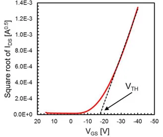
The charge carrier mobility in saturation region can be also evaluated from the plot of square-root of drain-source current versus the gate-source voltage. Moreover, the intercept point of this plot with x-axis provides a rough estimation of the threshold voltage as shown in Fig. 2.7.
Fig. 2.7. Square-root of IDS current versus VGS voltage for a typical
31
It is important to notice that charge carrier mobility in OTFT is a function of gate voltage [11] [12]. According to the model reported in [11], applying a voltage between gate and source terminals charge carriers are induced in organic semiconductor and they are trapped in numerous traps and only a fraction of charge carriers contribute to current conduction. The relationship between mobility and gate-source voltage [11] is given by the following equation:
2.6 = −
Where γ and VAA are empirical parameter that can be
extracted from the OTFT transfer characteristic and µ0 is a
constant.
Another important parameter for the OTFT is ION/IOFF
current ratio; it is defined as the ratio between the transistor current in accumulation mode and the transistor current in depletion mode. The ION/IOFF current ratio is essential for
evaluating the performance of OTFT when it is used as switch. Values as high as 107 were reported by recent OTFT
32
Fig. 2.8. Transfer characteristics of a p-type OTFT on logarithmic scale.
ION/IOFF ratio and subthreshold slope (SS) can be extracted
by the plot of drain-source current in saturation regime on a logarithmic scale versus the gate-source voltage as shown in Fig. 2.8.
Typically, the research activity on OTFT seeks to optimize two of the most important transistor parameters that are charge carrier mobility and ION/IOFF ratio.
33
2.1.3 Organic TFT structures
Organic TFTs are basically made using only five layers, i.e. substrate, semiconductor layer, source/drain layer, dielectric layer and gate layer. Their performance is affected by both physical and chemical layer properties as well as from the order in which each layer is deposited on substrate.
Basically, there are four main organic TFT structures: Bottom Gate-Bottom Contact (BG-BC), Bottom Gate-Top Contact (BG-TC), Top Gate-Top Contact (TG-TC) and Top Gate-Bottom Contact (TG-BC). In all structures the Source/Drain electrode has to be in contact with organic semiconductor to inject and retrieve charge carriers and the gate layer has to be isolated from organic semiconductor by means of dielectric layer. Pros and cons of each structure are highlighted in the following sections.
2.1.3.1 Bottom Gate – Bottom Contact
It is the commonly used structure for fabricating OTFT since organic semiconductor is deposited without limit on previous steps, see Fig. 2.9. Source/drain and gate electrode can be made using photolithographic patterning. Instead, gate dielectric can be deposited using different methods, i.e. plasma-enhanced chemical vapor deposition, RF magnetron sputtering.
34
Fig. 2.9. Bottom Gate – Bottom Contact structure (BG-BC).
One of the main disadvantages of BG-BC structure is the large contact resistance due to the small effective area for charge injection into the transistor channel. Moreover, during organic semiconductor deposition its morphology is disrupted because it goes in contact with two different materials, i.e. gate dielectric and source/drain electrode, simultaneously. As a result, BG-BC structure is characterized by large source/drain contact barriers and contact resistance.
2.1.3.2 Bottom Gate – Top Contact
BG-TC structures (Fig. 2.10) typically show a lower contact resistance respect to the BC structure thanks to the larger effective area where charges are injected into the organic semiconductor. This area is equal to the overlap area of source/drain electrode with organic semiconductor.
35
Fig. 2.10. Bottom Gate – Top Contact structure (BG-TC).
In this structure charge carriers that represent the transistor channel are induced on the opposite side respect to the source/drain electrodes. Thus, the charge carriers have to pass through an undoped highly resistive organic semiconductor layer. Mobility and threshold voltage of OTFTs made using this configuration may show a dependence on the thickness of the organic semiconductor layer.
Moreover, a photolithographic patterning cannot be made on organic semiconductor since organic semiconductor can be damaged; this means that source/drain electrodes have to be deposited using techniques with a lower resolution limiting the minimum transistor channel length.
2.1.3.3 Top Gate – Top Contact
This structure (Fig. 2.11) is not used because it is affected to a large contact resistance due to the small effective area in
36
which charge carriers are injected into the organic semiconductor for creating the transistor channel.
Fig. 2.11. Top Gate – Top Contact structure (TG-TC).
In this configuration, source/drain electrodes and gate dielectric are deposited on organic semiconductor layer. For this reason gate dielectric construction cannot be made using physical deposition methods such as sputtering due to the damages on organic semiconductor layer caused by the energetic ion during deposition. Moreover, for the same reason, photolithography techniques cannot be used for fabrication of source/drain electrodes.
In this structure gate dielectric encapsulate the organic semiconductor protecting it from oxygen and air exposure that can cause the degradation of organic semiconductor.
37
2.1.3.4 Top Gate – Bottom Contact
In this structure (Fig. 2.12) gate dielectric and gate electrode encapsulate organic semiconductor layer protecting it from any degradation processes.
Fig. 2.12. Top Gate – Bottom Contact structure (TG-BC).
On the other hand, there are many challenges that have to be overcome during the integration of this structure.
As first thing, gate dielectric and gate electrode have to be fabricated on organic semiconductor layer avoiding any damages to the organic material.
As second thing, any vertical interconnections between gate and source/drain electrodes have to be made through the organic semiconductor and hence fabrication processes that do not damage organic material have to be used.
38
As third thing, the deposition of gate dielectric on organic semiconductor can damage or unintentionally dope it by affecting on the performance of OTFT in terms of ION/IOFF
ratio.
TG-BC structure is characterized by a low contact resistance because the effective area for injecting of the charge carriers into the organic semiconductor is quite large; source/drain electrodes are embedded into the organic material.
High resolution and integration of organic TFT can be achieved because photolithographic pattering can be used for fabricating gate and source drain electrodes.
2.2 Fully-printed organic complementary
technology on flexible substrate
Circuits and systems reported in this thesis work were fabricated using the fully-printed complementary organic technology on flexible substrate developed by CEA-LITEN, Grenoble, France [10] [13-15].
Circuits fabrication is carried out on 11 cm x 11 cm flexible substrate, see Fig. 2.13. The organic complementary thin-film transistors (C-OTFT) are implemented in a top-gate bottom-contact multi-finger structure with a minimum
39
channel width (W) and length (L) of 140 µm and 5 µm, respectively. The technology process also features metal-insulator-metal (MIM) capacitors with a specific capacitance of 20 pF/mm2, which are built by using source/drain metal layer, gate dielectric layer and gate metal layer. Thanks to an additional process step, resistors with a sheet resistance of 35 kΩ/sq can also be integrated by screen-printing a carbon-ink after the organic semiconductor deposition and before the screen-printing of gate metal layer.
Fig. 2.13. Picture of 11 cm x 11 cm flexible foil with fully-printed OTFTs and digital and analog CMOS basic building blocks.
40
The OTFT cross-section and a microphotograph of an OTFT with a W=2000 µm and L=20 µm are shown in Figs. 2.14 and 2.15, respectively.
Fig. 2.14. Transistor cross-section of the fully-printed organic complementary technology on flexible substrate developed by CEA.
Fig. 2.15. Microphotograph of a multi-finger OTFT with a W=2000 µm and L=20 µm fabricated by CEA.
The fabrication process is characterized by few steps, see Fig. 2.16. It starts from a 125 µm thick polyethylene-naphtalate (PEN) foil that is a robust and flexible substrate. The first step consists of a sputtering of a 30 nm gold layer
41
that is then patterned using photolithography or laser ablation processes for realizing the source/drain electrodes as well as the first metal layer for interconnection.
N-type organic semiconductor is deposited before the p-type one. In the second step, the deposition of n-p-type organic semiconductor is preceded by the deposition of the Self-Assembled Monolayer (SAM) useful for the optimization of the electron injection in the Lowest Unoccupied Molecular Orbital (LUMO) [16]. The n-type organic semiconductor is patterned by means of printing method leading to create a final thickness in the range from 50 nm to 200 nm.
In the third step, a cleaning process with O2 UV free
plasma during 180 s is carried out in order to prepare the type area and the substrate for the deposition of SAM and p-type organic semiconductor. Also in this case, p-p-type material has a thickness in the range from 50 nm to 200 nm.
In the fourth step, the common fluoropolymer dielectric (CYTOP) that is the gate dielectric is deposited using the screen-printing technique on top of both semiconductors. The dielectric layer is then annealed reaching a final thickness of 750 nm. At the end, the gate electrodes and the second metal layer for interconnection are fabricated using a silver-ink conductor paste that is screen-printed and annealed at 100 °C.
42
In Fig. 2.16 is shown a simplified and schematic view of the fabrication process steps.
Fig. 2.16. Schematic view of the fabrication process steps of the fully-printed complementary organic technology on flexible substrate developed by CEA.
Two different process generations (GEN1 [13] and GEN2 [10], respectively) were developed by CEA-LITEN. The process flow above described refers to the latest process GEN2 that shows better performance respect to the GEN1 thanks to an additional optimization step based on a cleaning process with O2 UV free plasma for a time of 180 s. As
43
clearly reported in [10], the optimization process guarantees better stability and repeatability of transistor’s performance as well as a higher process yield.
Table 2.2 summarizes the measured electrical characteristics of both p-type and n-type OTFT, fabricated using GEN2 process flow, with a channel width and channel length of 2000 µm and 20 µm, respectively.
p-OTFT n-OTFT µSAT [cm 2 /V·s] 1.5 0.55 ION/IOFF ratio 10 4 2·105 Subthreshold Slope [V/decade] 4 2
VTH(SAT) [V] -22 18
Table 2.2. Measured electrical characteristics of both p-type and n-type OTFT with W=2000 µm and L=20 µm.
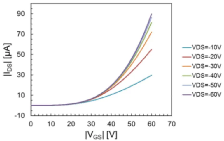
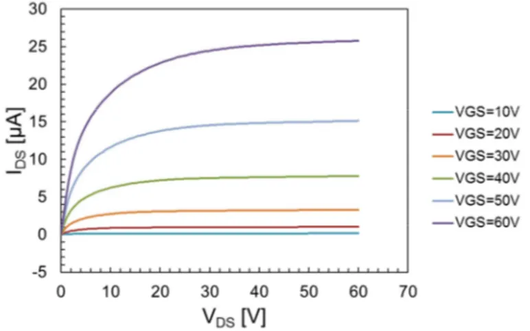
Output and transfer characteristics of GEN2 p-type and n-type transistors with channel width and length of 2000 µm and 20 µm are reported in Figs. 2.17, 2.18, 2.19 and 2.20, respectively.
A dedicated compact transistor model was developed for this technology [17]. This model is physically based and can describe both n-type and p-type OTFTs. The electrical
44
characteristics of transistor are basically modeled as a series of an “ideal transistor” and a reverse biased Schottky diode.
Fig. 2.17. Output characteristics of p-type OTFT with channel width and length of 2000 µm and 20 µm, respectively.
Fig. 2.18. Transfer characteristics of p-type OTFT with channel width and length of 2000 µm and 20 µm, respectively.
45
Fig. 2.19. Output characteristics of n-type OTFT with channel width and length of 2000 µm and 20 µm, respectively.
Fig. 2.20. Transfer characteristic of n-type OTFT with channel width and length of 2000 µm and 20 µm, respectively.
46
2.3 Digital and analog basic building blocks
Several digital and analog basic building blocks were designed using OTFT manufactured in a fully-printed complementary organic technology on flexible substrate. The main technology characteristics were already presented in the previous paragraph (¶ 2.2).Circuits design was carried out by taking advantage of the dedicated transistor model in [17].
In the following section, measurements of seven stage ring oscillator and fully-static logic gates such as inverters, NAND gate and J/K flip-flop are reported. Moreover, measured results of first dynamic NAND gate and positive edge triggered TSPC D flip-flop are also presented.
Finally, measurements of differential gain stage with active load and a complete characterization of simple rectifier/envelope detector up to 13.56-MHz are also discussed.
2.3.1 Static CMOS inverter and NAND gate
Most of the published organic logic gates were fabricated using only p-type OTFTs. They are mainly based on ratioed logic architecture in which the pull-down network is made up of a diode-connected p-type transistor or by using a zero-VGS
47
load [18]. Moreover, a new design logic named PMOS-only
Pre-Discharge logic was also proposed in [19] to implement
logic functions. It uses mostly p-type OTFTs based on principles of dynamic logic.
The availability of complementary technology that integrate both p-type and n-type OTFTs allows implementation of static CMOS logic gates that show better performance in terms of power dissipation, noise margin as well as less required area for integration respect to the ratioed logic gates.
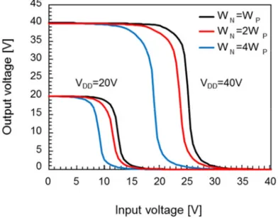
Fig. 2.21. Symbol, truth table and schematic of a static CMOS inverter.
![Fig. 2.1. Historic progress in the performance and maximum reported carrier mobility of organic TFTs [6]](https://thumb-eu.123doks.com/thumbv2/123dokorg/4473504.32036/47.630.160.478.406.710/historic-progress-performance-maximum-reported-carrier-mobility-organic.webp)