XXV CICLO DEL CORSO DI DOTTORATO
Metamaterials and plasmonics for novel components
at microwave and optical frequencies
(Metamateriali e materiali plasmonici per la progettazione di componenti innovativi a microonde e frequenze ottiche)
Dottorando:
Ing. Davide Ramaccia
To the most exciting, fast growing, and fully challenging area. METAMATERIALS.
Acknowledgements
This research project was carried out at the Department of Applied Electronics (DEA), “RomaTre” University, Rome, Italy, from January 2010 to December 2012.
Firstly, I owe my sincere gratitude to my supervisor Professor Alessandro Toscano, Head of the Electromagnetic Diagnostic Laboratory, for his support and guide during my research in metamaterial field. Moreover, I express my special appreciation to him for giving me autonomy and responsibilities.
I wish to express my warmest thanks to Professor Filiberto Bilotti for valuable ideas and introduction to scientific work. His enthusiasm and trust in me sustained my research project through difficulties. He deserves all my heartfelt gratitude and deepest thanks for his formative and congenial support in posing and solving advanced electromagnetic problems, and the fortunate liberty to collaborate with many people and institutions.
I cordially express my thankfulness to Professor Giorgio Guattari, Head of Department of Applied Electronics, for the excellent conditions, and pleasant working environment at the Department.
Also, I render thanks to Dr. Alessio Monti and Dr. Mirko Barbuto, research mates at the Applied Electromagnetic Laboratory, for the wonderful days spent in the laboratory between pure research work and enjoyments.
Finally, I want to reserve a special word of gratitude to my parents, girlfriend Roberta and friends for their love, enthusiastic encouragements, and a huge variety of other reasons.
Contents
Esteso Sommario (Italiano) vi
Introduction xi
1 Metasurfaces with electrically small circular inclusions 1
1.1 Introduction...2
1.2 Partially reflective surface...2
1.3 High impedance surface...13
1.4 References ...29
2 Metamaterial-based filter element for waveguide applications 33 2.1 Introduction...34
2.2 The bi-omega particle ...36
2.3 Connected bi-omega particle ...43
2.4 Metamaterial-inspired waveguide filter ...46
2.5 Self-filtering horn antenna ...51
2.6 Waveguide power splitters ...56
2.7 References ...61
3 ENZ metamaterial lens for novel aperture antennas 64 3.1 Introduction...65
3.3 Horn antennas with steerable beam ...84
3.4 References ...91
4 Guiding and radiating components at IR and optical frequencies 96 4.1 Introduction...97
4.2 Silver MIM nano-waveguide with pillars ...99
4.3 Horn nano-antenna: design and performaces ...102
4.4 References ...105
List of Figures and Tables 107
Publications and presentations 113
Esteso Sommario
(Italiano)
Introduzione
Negli ultimi cento anni, l’elettromagnetismo è stata ampiamente impiegato per comprendere a fondo l'interazione con la materia a qualsiasi scala, dalla cosmologica fino ai fenomeni su scala atomica. La teoria elettromagnetica classica è anche alla base di molte applicazioni pratiche che influenzano fortemente la vita di tutti i giorni. Sembra quindi molto difficile aggiungere qualcosa di concettualmente nuovo a tali teorie e tecnologie ben consolidate. Tuttavia, circa dieci anni fa, un nuovo concetto apparso nell'universo della teoria elettromagnetica classica: metamateriale.
Che cosa è un "metamateriale"? Si tratta di un materiale artificiale opportunamente ingegnerizzato la cui risposta elettromagnetica non è facilmente reperibile in natura. Per esempio, i metamateriali possono presentare valori negativi della permettività elettrica della permeabilità magnetica, o entrambi, in un certo intervallo di frequenza delle microonde. La risposta non convenzionale di questi metamateriali è ottenuta attraverso inclusioni metalliche elettricamente piccole o disomogeneità dielettriche in un mezzo dielettrico ospite. Le proprietà esotiche di metamateriali possono essere previste utilizzando approcci quasi-statici e considerando l'interazione tra le diverse inclusioni disposte in un reticolo tridimensionale. Anche se l'interazione tra onde elettromagnetiche e la materia è un tema di ricerca della Fisica, le relative applicazioni sono ampiamente studiati nell’ Ingegneria Elettrica ed Elettronica. Pertanto, i metamateriali hanno contribuito a colmare il divario tra queste due comunità e ora i fisici e gli ingegneri lavorano insieme su questo tema. L'attuale interesse dei metamateriali è dovuto alla loro capacità di presentare le proprietà elettromagnetiche inedite utili in diversi campi applicativi. Utilizzando i metamateriali, infatti, è possibile modificare quasi a volontà le proprietà delle onde elettromagnetiche.
Aumentando la frequenza del campo elettromagnetico, alcune delle proprietà insolite appena citate sono già date dalla natura, anche se è sempre possibile ingegnerizzarle attraverso appropriate tecnologie di fabbricazione su scala nanometrica. Ad esempio, a
frequenze ottiche, la natura ci dà i materiali plasmonici. I materiali plasmonici sono semplicemente metalli nobili, come oro o argento, che alle frequenze ottiche consentono la propagazione delle onde superficiali estremamente confinate all'interfaccia metallo-dielettrico. La propagazione è data dalla oscillazione collettiva degli elettroni all'interno del metallo che sono eccitati dal campo esterno. Per spiegare tale comportamento anomalo, i metalli sono descritti come materiali dielettrici ed è stato dimostrato che tale propagazione avviene solo se la permittività efficace, o permittività ottica, del metallo è negativa, proprio come i metamateriali alle microonde.
In questo scenario, è evidente che metamateriali e materiali plasmonici possono aprire molte sfide di interesse per i fisici e gli scienziati in generale. Dal punto di vista tecnologico, l'interesse per tali materiali si basa sulla possibilità di progettare dispositivi e sistemi con nuove proprietà o funzionalità, in grado di aprire nuovi campi di applicazione o per migliorare le prestazioni di quelli già esistenti.
In questa tesi, vorrei raccogliere i risultati della mia ricerca per l'impiego di metamateriali e materiali plasmonici per la progettazione di nuovi componenti a microonde e frequenze ottiche. Nel capitolo 1 sono riportati i modelli analitici per l'analisi di metasurfici con inclusioni elettricamente piccole. Queste sono stati utilizzate per realizzare superfici parzialmente riflettenti (PRS) e superfici ad alta impedenza (HIS) per applicazioni in polarizzazione circolare. Capitolo 2 è focalizzato sulla progettazione di un elemento filtrante basato su metamateriale impiegato per la realizzazione di nuovi e compatti componenti a microonde per la guida e la radiazione di campo elettromagnetico. Capitolo 3 è dedicato ai metamateriali ENZ (epsilon-near-zero) e le loro applicazioni in antenne a tromba. Infine, il capitolo 4 è dedicato ai materiali plasmonici che sono stati impiegati per la progettazione di un guida d'onda e una antenna a tromba che lavorano a frequenze ottiche.
In tutti i capitoli, ho riportato lo stato dell’arte sul tema particolare del capitolo e incluso una combinazione di risultati teorici, numerici e sperimentali per la comprensione del comportamento dei metamateriali nella particolare applicazione considerata.
1 Metasuperfici con inclusioni elettricamente piccole
In questo capitolo, è presenta l'analisi e la progettazione di un metasurface costituita da una serie di inclusioni circolari allineate lungo le due direzioni principali del piano della superficie con periodicità inferiore alla lunghezza d'onda. Il modello proposto è stato applicato ad una parete metallica su cui sono stati effettuati dei fori circolari e anche a una serie di patch circolari stampati su un substrato dielettrico elettricamente sottile elettricamente. La prima configurazione realizzare una superficie parzialmente riflettente che induce un onda leaky ed un effetto di beam-forming quando è posta di fronte a una antenna ad apertura, o una antenna a patch, o a un qualsiasi radiatore standard. Il guadagno e larghezza di banda dipendono dalla riflessione (ampiezza e fase) del superficie nonché la distanza dal radiatore stesso. Al contrario, la seconda configurazione è nota come superficie ad alta impedenza ed è posta indietro al radiatore. Poiché le dimensioni sono di molto inferiori alla lunghezza d'onda, l’array di patch e il substrato possono essere descritti in termini di una capacità e una induttanza concentrata, rispettivamente. Intorno alla frequenza di risonanza, la superficie riflette totalmente un'onda elettromagnetica incidente con uno sfasamento nullo. Grazie a questa proprietà, è ampiamente impiegata in sistemi di antenna come riflettore posteriore compatto con migliori prestazioni rispetto al riflettore tipico metallo.
2 Elemento filtrante basato su metamateriale
In questo capitolo, è riportato il modello analitico della particella bi-omega composta da due risonatori ad omega orientati in verso opposto ed opportunamente distanziati. Posizionando le due particelle ad omega molto vicine, l'effetto di accoppiamento tra di loro contribuisce a spostare verso il basso la frequenza di risonanza, ottenendo un risonatore semplice ed elettricamente piccolo che lavora nella gamma delle microonde. Il modello proposto, basato sulla teoria delle antenna piccole, tiene conto di tutti gli effetti di accoppiamento che entrano in gioco quando la distanza tra le due omega è molto piccola. Poi, due particelle bi-omega sono collegate tra loro, al fine di ottenere un trasferimento di energia da un bi-omega, usata come antenna ricevente, e l'altra, l'antenna trasmittente, quando è collocata in una fenditura in uno schermo metallico.
Grazie al suo comportamento risonante, la struttura proposta può essere usato con successo come filtro passa-banda in grado di selezionare la frequenza di interesse con elevata precisione, che è fortemente richiesto in molte applicazioni di guida d'onda e antenne apertura. Tra questi, è presentata la progettazione e la realizzazione sperimentale di componenti a microonde innovative, come ad esempio i filtri in guida d'onda, diplexer, power-splitter, filtri modali, antenne a tromba, ecc I componenti proposti sono verificati attraverso adeguate simulazioni numeriche full-wave e risultati sperimentali.
3 Metamateriali ENZ per antenne ad apertura innovative
In questo capitolo, sono presenti due nuovi layout di lente piatte, costituite da materiale convenzionale e da un metamateriale ENZ (epsilon-near-zero) o da un metamateriale ENZ caricato con induttori. Entrambe le configurazioni sono utilizzate come plug sulle aperture di antenne a tromba, al fine di ottenere nuove prestazioni in radiazione .
In primo luogo, è presentata una lente in metamateriale per antenne ad apertura accorciate che permette di raggiungere su un'ampia gamma di frequenze prestazioni radianti simili a quelle delle antenne corrispondenti con lunghezza ottimale. In funzionamento è basato sul concetto di compensazione di fase: la fase del fronte di campo propagante all’interno della antenna a tromba si propaga con differenti velocità di fase nei due materiali della lente, presentandosi poi con una fase uniforme all’uscita della lente stessa. Inoltre è presentata una versione realistica della lente, realizzata con un allineamento di fili metallici che esibiscono una permittività effettiva vicino allo zero nella gamma di frequenze di interesse. Considerando due esempi in banda C, si dimostra che la lente può essere progettata per antenne a tromba sia coniche che piramidali. In entrambi i casi, la lunghezza delle horn è metà delle corrispondenti versioni ottime, mentre le prestazioni di radiazione ottenute sono simili a quelle delle horn ottime su una banda di frequenza molto ampia.
Successivamente, sono riportati i risultati numerici di una antenna a tromba con diagramma di radiazione orientabile. La rotazione del massimo del diagramma di
radiazione è ottenuta modificando localmente l'indice di rifrazione della lente ENZ al fine di modificare localmente la lunghezza elettrica della lente stessa.
4 Guida d’onda e antenna ad apertura a frequenze ottiche
In questo capitolo, sono stati discussi il design e le prestazioni di una guida d'onda ottica e di una antenna a tromba che lavorano alle frequenze vicine all'infrarosso. Per prima cosa, è stata progettata la guida d'onda a scala nanometrica, che dovrebbe soddisfare alcuni requisiti importanti per essere una buona guida d'onda: da un lato, dove guidare efficacemente la luce e, dall'altro, dove presentare una topologia che è simile alla sua controparte alle frequenze delle microonde. Quindi ci si è basati su una linea di trasmissione simmetrica costituito da una lastra di materiale non plasmonico tra due strati plasmonici. Tale struttura supporta un modo fondamentale che si propaga tyra i due strati metallici e presenta una forte componente di campo elettrico ortogonale ad essi.Successivamente, si considera il problema della radiazione efficace del campo elettromagnetico guidato. Di recente il concetto di antenna è stato trasferito dalle microonde all’ottica, per via delle possibili applicazioni nella raccolta di energia, nell’ illuminazione intelligente, e nei collegamenti ottici per la comunicazione senza fili. Inoltre, i recenti progressi nella nano-tecnologia rendono la possibile realizzazione di tali dispositivi. Quindi, è riportato il progetto di una nano-antenna ottica ottenuta sagomando ad una delle estremità della guida d'onda ottica in modo tale da aumentare l'apertura fisica e progressivamente adattare l’impedenza d’onda all’impedenza dello spazio libero.
Introduction
In the last century, electromagnetic theory has been widely employed to deeply understand the interaction with matter at any scale, from cosmological down to atomic scale related phenomena. Classic electromagnetic theory is also the base of many practical applications which strongly influence everyday life.
It seems very difficult, thus, to add something conceptually new to such well-established theories and technologies. However, around ten years ago, a new concept appeared in the universe of classical electromagnetic theory: metamaterials.
What is a “metamaterial”? It is an artificially engineered material whose electromagnetic response is not readily available in nature. For instance, metamaterials can exhibit negative values of the electric permittivity of the magnetic permeability or both in a certain microwave frequency range. The unconventional response of these metamaterials is obtained through electrically small metallic inclusions or dielectric inhomogeneities within a dielectric host medium. The exotic properties of metamaterials can be predicted by using quasi-static approaches and considering the interaction among the different inclusions arranged in a 3D lattice. Although the interaction between electromagnetic waves and matter is a hot research topic in Physics, the related applications are widely studied in Electrical and Electronic Engineering. Therefore, metamaterials helped to bridge the gap between these two communities and now physicists and engineers work together on these topics. The current interest in metamaterials is driven by their potential to obtain unprecedented electromagnetic properties useful in several application fields. By using metamaterials, in fact, it is possible to tailor the wave properties almost at will.
Increasing the frequency of the electromagnetic field, some unusual properties are already given by nature, though it is always possible to engineer them through proper nano-scale fabrication technologies. For example, at optical frequencies, nature gives us the plasmonic materials. The plasmonic materials are simply noble metals, such as gold or silver, that at optical frequencies allow the propagation of surface waves extremely confined at the metal-dielectric interface. The propagation is given by the collective oscillation of the electrons inside the metal that are excited by the external impinging
field. In order to explain such anomalous behavior, metals are described as dielectric materials and it has been shown that such propagation takes place only if the effective permittivity, or optical permittivity, of metal is negative, just as the metamaterials at the microwaves.
With this scenario, it is evident that metamaterials and plasmonic materials may open many challenges of interest to physicists and scientists in general. From the technological and engineering viewpoint, the interest in such materials is based on the possibility of designing devices and systems with new properties or functionalities, able to open up new fields of application or to improve existing ones
In this dissertation, I would like to collect the results of my research on the employment of metamaterials and plasmonic materials for the design of novel components at microwave and optical frequencies. Chapter 1 develops the analytical models for the analysis of metasurfaces with electrically small inclusions. They have been used to realize Partially Reflective Surfaces (PRS) and High-Impedance Surfaces (HIS) for circular polarization applications in antenna field. Chapter 2 is focused on the design of a metamaterial-based filter element employed for the realization of novel compact guiding and radiating microwave components. Chapter 3 is devoted to the epsilon-near zero (ENZ) metamaterials and their applications in horn antennas. Finally, Chapter 4 is devoted to plasmonic materials exploited to design a nano-waveguide, acting as its microwave counterpart, and an innovative horn nano-antenna working at near-infrared and optical frequencies.
In all chapters, I have reported the state-of-the-art on the particular topic of the chapter and included a combination of theoretical, numerical, and experimental results to the understanding of the behavior of metamaterials in the particular considered application.
1 Metasurfaces
with electrically small circular
inclusions
In this chapter, I present the analysis and design of a metasurface consisting of an array of circular inclusions with a sub-wavelength periodicity. The proposed study is suitable for circular holes in a metal conducting sheet, as well as metallic circular patches printed on a electrically thin metal-backed dielectric substrate. The first configuration realize a Partially Reflective Surface (PRS) that introduces a leaky wave and beam-forming effect when placed in front of a grounded waveguide aperture, patch antenna, or any standard radiator. The gain and bandwidth depend on the reflection (amplitude and phase) from the PRS as well as the distance from the radiator itself. On the contrary, the second configuration is known as High-Impedance Surface (HIS) and it is placed back to the radiator. Since the sub-wavelength dimensions, the array and the metal-backed substrate can be described in terms of a lumped capacitance and a lumped inductance, respectively. Around the resonant frequency, the HIS reflects totally an incident electromagnetic wave with zero shift in phase. Due to this property, it is widely employed in antenna systems as compact back reflector with improved performances with respect to typical metal reflector.
In order to validate the analytical results, I compare the analytical results to the ones resulting from full-wave numerical simulations and from other analytical methods available in the open technical literature.
1.1 Introduction
In the past two decades, the development of wireless communication systems has been possible thanks to significant progress in the fields of electronics and applied electromagnetics. Device miniaturization, superior performances with respect to the state-of-the-art solutions, and low production costs represent the main challenges driving current academic and industry efforts. For what concerns the radiating segment of wireless systems, miniaturization and low-cost solutions are commonly achieved exploiting microstrip printed technology. In order to enhance the performances and reduce the size of the radiating systems, antennas can be properly loaded by artificial materials or surfaces [1]-[5], among which include the so-called metamaterials and metasurfaces [6]-[14]. These engineered materials and surfaces exhibit electromagnetic properties that cannot be found in nature. The recent developments in the field of metamaterials and metasurfaces have led to innovative designs of radiating and transmitting components [4]-[10].
In this chapter, the analytical study of two metasurfaces, i.e. a partially reflected surface and an high impedance surface, with electrically small circular inclusions will be presented.
1.2 Partially reflective surface
In this section, I present a study on a metasurface consisting of a planar array of sub-wavelength circular apertures drilled in a perfect conducting metallic sheet. Possible applications of such structures include artificial dielectrics, antenna radomes, frequency selective surfaces, etc. Particularly, their use is highly desired in antenna applications, allowing to: a) enhance the directivity of the radiators, increasing their effective radiating area; b) reduce the back-radiation and the wind resistance when used as reflectors. Interesting examples of applications to enhance the antenna directivity are reported in [13]-[15].
Being the dimensions of the array elements much smaller compared to the operating wavelength, an effective boundary condition can be used to describe the electromagnetic behavior of the metasurface. By defining an average value of the tangential electric field and of the surface current density on the array plane, in fact, it is possible to introduce an effective grid impedance Zg describing the electrical properties of the structure [16]-[20].
In the open technical literature the analysis of metasurface composed by two sets of crossed metallic strips has been already presented. When this surface is excited by an electromagnetic plane-wave, the surface current density is uniform along the strips parallel to the electric field vector. On the contrary, when circular holes are considered, the current distribution on the metallic region between two adjacent circular apertures varies according to the local width of the metal. Since the operating wavelength is assumed much larger than the periodicity, a quasi-static approach can be used to describe the electromagnetic behavior of the structure and the current density distribution should depend only on the geometrical parameters of the metallic regions. Considering a square lattice for the aperture arrangement, the structure can be seen as a grid of metal strips with non-constant width where the surface current flows.
Using this approach, the analytical formulas already developed for the grid impedance of a grid of metallic strips with constant width [21] can be properly modified in order to accurately describe the behavior of the considered structure. The new proposed model is verified comparing the obtained reflection coefficient to the one resulting from full-wave numerical simulations based on the employment of CST Studio Suite [22]. According to [23], we have simulated just one unit-cell using proper boundary conditions. As a further reference, we consider also the results given by other accurate analytical models available in the open technical literature and based on the polarizability of the inclusions [16].
In the following, I briefly introduce the approach to the problem and present the analytical method used to evaluate the effective width of the equivalent grid of metal strips. Then, I compare the amplitude of the reflection coefficients for TE and TM polarizations obtained through our model, other models, and full-wave results. Finally, I
draw the conclusions and highlight, under the validity limitations, the advantages of our proposed approach.
1.2.1 Analysis and design of PRS
When a plane-wave impinges on a metallic surface, the tangential components of the electric and magnetic fields excite an uniform surface current density. The electric field reflected by the surface experiences a 180° phase-shift, due to the reaction of the surface. Under the same illumination conditions, the surface current density on a metasurface consisting of an array of sub-wavelength circular apertures is not uniform, but rather shows high values in the metallic regions with minimum width between two adjacent holes (Fig. 1a).
Fig. 1: Representation of the surface current and concatenated magnetic field
for an array of (a) circular holes in a metallic sheet and (b) metallic strips; (c) Map of the magnitude of the surface current for k S0 0.5 and R0.45 S.
Investigating the distribution of the surface current density, we observe that its maximum value is in correspondence of the minimum width of the metallic region between two holes and it decreases moving away from this point (Fig. 1). Since the
operating wavelength is much larger than the periodicity of the structure, the unit-cell is assumed as excited by a quasi-static electromagnetic field. In this case, the current density distribution should depend only on the width of the metallic region in x-direction (see Fig. 1a). On the contrary, on metasurface consisting of squared apertures the surface current density is quite constant on the metallic strips between two adjacent squared holes (see Fig. 1b). Starting from this approach, we apply the integral mean value theorem over the metallic region between two circular holes, evaluating an effective width weff in order to model it as an equivalent array of sub-wavelength squared holes.
In Fig. 2, a zoom on the metallic region between two adjacent circular patches is shown. The integrating area A is vertically defined by the angle and horizontally delimited by the edges of the holes .
Fig. 2: Integrating region between two adjacent holes.
The area A can be expressed in terms of the periodicity S, the radius R of the holes, and the height y as follows:0
2 1 0 2 2 0 0 0 2 2 0 y S 1 A y R tan y R y 2 2 R y (1)
where y0 R sin. Dividing the area A by y , an average value of the width of the0 metallic region between the two holes as a function of the angle can be found as:
eff w S R cos sin (2)According to the polarization and to the angle of incidence of the incoming wave, the area of the metallic region involved in the flow of the current changes and consequently the effective width of the equivalent strips too. The height y , that is directly related to0 the angle , defines the extension of the area A. In order to evaluate a constant value of the effective width weff, we define the values of the angle for TE and TM polarization (Fig. 3).
Fig. 3: Oblique incidence: (a) TE polarization; (b) TM polarization.
For TE polarization, the electric field is parallel to the array plane whatever the angle of incidence is, as shown in Fig. 3a. In this case, the metallic region involved in the flow of the current density is maximum and defined by the angle:
TE
2
(3)
For TM polarization, the tangential component of the incident electric field is
0cos
t
decreases with the angle of incidence. The metallic region A (Fig. 2), thus, should decrease as function of the incident angle , accordingly. In this case, the metallic region involved in the flow of the current varies with the angle of incidence and is defined by the angle:
TM cos2
2
(4)
where the quadratic dependence is justified by the fact that the angle defines the coordinate y that in the circumference equation appears in a quadratic form.0
Inserting eqs. (3), (4) into (2), we obtain the constant effective width of an equivalent array of metallic strips for both polarizations. It now can be used in the readily available analytical formulas of the grid impedance of an array of metal strips [17]-[18], [21] and we obtain the grid impedance of an array of circular holes in a metal sheet:
holes TE TE 0 1 eff g 0 k S w Z jZ ln sin 2 2S (5) holes TM 2 TM 0 1 eff g 0 k S w sin Z jZ ln sin 1 2 2S 2 (6)
where Z0 and k0 0 0 are the wave impedance and the wave vector in vacuum, respectively, and S is the periodicity of the array. The effective widths wTEeff and wTMeff are constant values evaluated using eq.(2) when the is TE and TM, respectively.
The validity of eqs. (5), (6) is guaranteed when the periodicity S of the structure is sub-wavelength and the effective width of the strips is much smaller than the periodicity [17]-[18], [21]. In order to keep the validity of the formulas after the introduced modifications, the dimensions of the holes should be comparable to the periodicity of the array.
1.2.2 Analytical and numerical results
The electromagnetic properties of the grid array can be expressed in terms of the transmission and reflection coefficients. If the metallic array is printed on a dielectric substrate, it is possible to define an effective permittivity of the surrounding host medium as described in [24]. Using a transmission line model, the shunt reactive impedance Zg modeling the array is connected to two infinitely extended transmission lines of impedance Z, as show in Fig. 4.
Fig. 4: Transmission–line model of a dense array in a uniform host medium.
If the host medium is the free-space, the characteristic impedance Z of the transmission lines is Z0 0 0. In case of oblique incidence, as show in Fig. 3, the free-space impedances are given by:
TE 0 0 TM 0 0 Z Z cos Z Z cos (7)
and the reflection coefficients are:
TE TM TE 0 TM 0 TE TE TM TM 0 g 0 g Z Z ; Z 2Z Z 2Z (8)
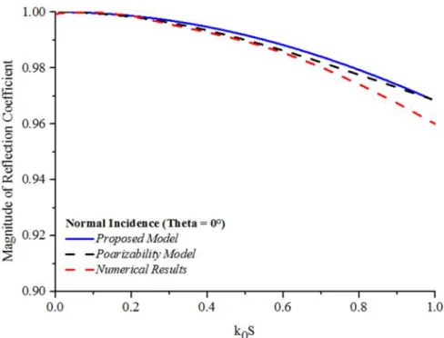
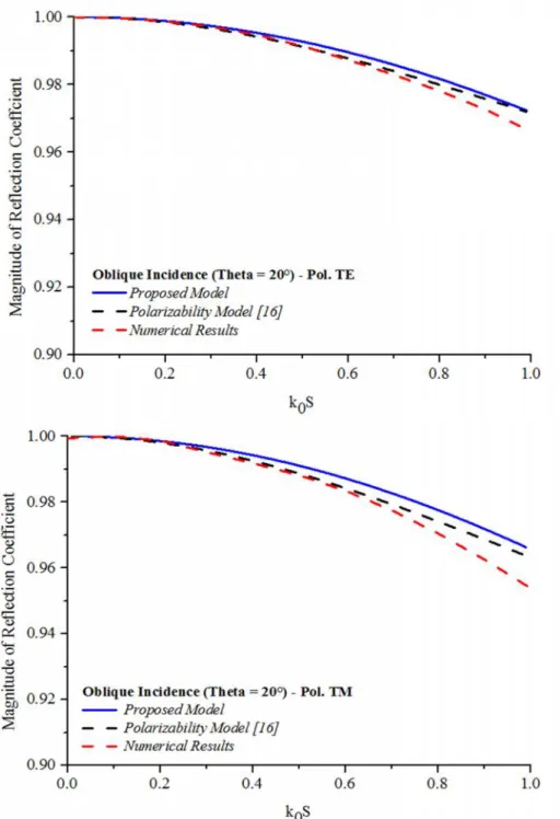
In Fig. 5, Fig. 6, and Fig. 7 the amplitude of the reflection coefficient versus the normalized period k S for different angles of incidence and both polarizations is0 shown. The radius R of the holes is set to R0.45 S. The solid lines represent the amplitude of the reflection coefficient of the array of circular holes in a metallic sheet modeled using the proposed method based on the effective width of the metallic strips. The hollow circles represent the results obtained through the full–wave numerical simulator CST Studio Suite [21]. The two sets of results agree reasonably well in all the reported cases.
For a further validation, we compare our model to the one presented in [16] for a complementary structure, i.e. an array of disks, after a proper application of Babinet’s principle (dot-line).
Fig. 6: Reflection coefficient vs. normalized periodicity at oblique incidence (θ = 20°) for both polarizations.
Fig. 7: Reflection coefficient vs. normalized periodicity at oblique incidence (θ = 40°) for both polarizations.
The agreement between the proposed model, based on the effective width, and the two references, i.e. the numerical simulations and the polarizability-based model, is rather good, showing the validity of the proposed approach.
1.2.3 Conclusions
In this section, a new analytical model for a partially reflective metasurface consisting of an array of circular holes in an ideally conducting sheet has been presented. Investigating the distribution of surface current density, we defined an effective width of the metallic region between two adjacent circular holes. The effective width has been inserted in the simple and compact formulas of the grid impedance of an array of metallic strips. After the reported successful comparison of the results obtained using this approach to the full-wave numerical simulations and other analytical results obtained using more involved and complex methods based on the derivation of the polarizability of the unit-cell, we can conclude that the new model we have developed can be straightforwardly employed for the accurate and fast design of metasurfaces, consisting of arrays of circular apertures in a metallic sheet. The proposed model has been shown to be robust for both polarizations and different angles of incidence.
Before concluding, we remark that the potential of the proposed model resides in the ability to be applied to more complex unit-cell shapes, such as ellipses, rounded bowties and rectangles with high axial ratio, etc. Using the same set of the equations for the grid impedance of regular metallic strips, in fact, the effective width can be straightforwardly evaluated for the different unit-cells, leading to an easy, fast, and accurate design of different metasurfaces. It is worth mentioning also that the methods based on the polarizability of the unit-cell particle, though accurate, need the evaluation of special functions, as reported for the circular case in [16], and, thus, are not readily applicable for a fast design, as our proposed method does.
1.3 High impedance surface
As previously mentioned in the introduction of the chapter, in order to enhance the performances and reduce the size of the radiating systems, antennas can be properly loaded by artificial materials or surfaces [1]-[3], [25], [26], among which include the so-called metamaterials and metasurfaces, exhibiting functionalizing properties [4], [6]-[9], [27]-[29]. For instance, in order to reduce the thickness of printed antennas and enhance the performances in terms of efficiency and gain, it is possible to use the concept of High-Impedance Surfaces (HISs) [30], capable of highly reduced propagation of surface waves trapped within the substrate. An HIS is a metasurface consisting of a planar array of metallic patches printed on a metal-backed dielectric substrate. Provided that the array periodicity is electrically small, as well as the dimension of the individual particle representing the array unit-cell, an HIS can be represented in terms of its homogenized surface impedance [30]. At and around its resonant frequency, an HIS approximately behaves as a perfect magnetic wall, leading to several interesting applications in the antenna field [30]-[34]. Shape and dimensions of the individual patch element represent the key parameters for the design of an HIS and the synthesis of its frequency response. Generally, patch elements are arranged in a dense array and exhibit squared [30], hexagonal [31], and rectangular [35] shapes.
In this paper, we refer to an HIS made of a grounded dielectric thin slab with a dense array of circular patches printed on top. Such a configuration is particularly appealing due to its 2D isotropic response on the array plane. The sub-wavelength periodicity of the array and thickness of the substrate, the structure can be studied in the quasi-static regime and consequently in terms of a lumped elements: the metallic patch array can be described as a capacitive reactance, the metal-backed substrate as a inductive one. The shape of the patch element affects the value of the capacitive reactance that need to be properly defined for the geometry under study, i.e. circular in this case. In the open technical literature, it is possible to find two different approaches in the open technical literature: the first considers the dense array as an frequency selective surfaces (FSSs) in long-wavelength regime [36], and the latter defines the electrically small individual patches in terms of an electric dipoles represented through its electric polarizability
[16], [17]. Both define a lumped impedance, that in the case of an array of perfect conducting metallic disks, is capacitive. The sub-wavelength-FSS-based model [36] is derived approximating the Floquet theory under the assumption that the periodicity is few tenths of the operating wavelength. On the contrary the polarizability–based model [16] assumes that the inclusions are so electrically small that they can be described in terms of an electric dipoles, losing the information about the geometry of the inclusion itself.
The aim, thus, is to propose a new model for the grid impedance of a planar array of circular disks that fills the gap between the two models used to evaluate the frequency behavior of an HIS. Starting from a detailed study of the near-field distribution of the electric field around the circular patches, we modify the analytical formulas already developed for the grid impedance of a squared-patch-based HIS [21], [37] in order to accurately describe the behavior of a circular-patch-based one. The new proposed model is validated considering its ability to reproduce the full-wave numerical results obtained through the commercial electromagnetic simulator CST Studio Suite [22]. As further comparison, we report the results of the frequency response estimated by the other models [16], [36].
In the following, I briefly review the model of an HIS and discuss the grid impedance of a circular-patch-based HIS, presenting the related analytical formulas. Then, I show the comparison between the resonant frequencies estimated using the proposed analytical model, the full-wave numerical simulator [22], the sub-wavelength-FSS-based model and the polarizability–based model.
1.3.1 Analysis and design of HIS
An HIS consisting of a regular array of circular patches is shown in Fig. 8. The surface is infinite in the x-y plane and the dielectric material considered is non-magnetic, i.e. its permeability is taken to be the free-space permeability . The0 thickness and the relative electric permittivity of the dielectric slab are h and ,r respectively. The period of the array is D in both directions. The metallic components
are assumed to have a negligible thickness. The radius of the patches is R, and g is the gap between two adjacent patches.
Fig. 8: Side and top views of an HIS made by a regular array of circular patches.
As well known, the frequency behavior of an HIS can be easily studied using the transmission line model shown in Fig. 9.
Fig. 9: Transmission line model of the structure reported in Fig.1.
The metal–backed dielectric slab is equivalent to a transmission line of length h and characteristic impedance Zd Z0 r , where Z0 377 is the free-space wave
impedance, terminated in a vanishing impedance ZL modeling the metallic ground plane. The shunt impedance Zg represents the averaged impedance of the grid [17], which is a meaningful parameter when the periodicity D is smaller than the operating wavelength. The total surface impedance of the HIS is given by the input impedance Zs resulting from the parallel connection between the grid impedance Zg and the line impedance Z: 1 s g 1 1 Z Z Z (9)
where the input impedance Z exhibits an anti-resonant behavior and the structures shows high values of the surface impedance at and around the resonant frequency.
In order to evaluate the grid impedance Zg, we investigate on the distribution of the electric charges on the array plane when it is illuminated by a plane wave in long-wavelength regime. As shown in Fig. 10, the electric charges are distributed along the curved edges of the metallic circular elements. In the region of minimum distance between the edges of two adjacent vertical patches the electric field amplitude is maximum.
Fig. 10: Map of the electric field amplitude on the plane of an array of circular patches. The exciting electric field is polarized along the y-direction.
The distribution of the electric field along the edge is more similar to the one of a squared patch that, under the same condition of excitation, is quite constant along the whole length. In the following we show that, by using a proper modification, the formulas, used for the squared patch case proposed in [21], can be effectively used also for the circular case.
In Fig. 11 I show the squared- and the circular-patch-based structures with the respective geometrical parameters. They have the same periodicity D and the same gap
g. The thickness and the electric permittivity of the dielectric slab are also the same. The
diameter 2R of the circular patches is equal to the length L of the edge of the squared patches.
Fig. 11: Side and top views of two High Impedance Surfaces consisting of a regular array of circular (left) and squared (right) patches.
When an uniform plane-wave impinges normally on the surface from the above, the grid impedance Zg of the HIS with squared patches is given by [17], [21], [37]:
eff g Z Z j 2 (10)
where is the grid parameter defined as:
eff k D 1 ln g sin 2D (11)
and Zeff Z0 eff , keff k0 eff are the wave impedance and the wave number in the effective medium, respectively, and eff is the effective permittivity of the space surrounding the array grid. In fact, according to [24], [38], it is possible to analyze the electromagnetic behavior of a structure at the interface between two dielectrics, one of which is the air, using an effective permittivity eff
r1 2
as if the array elements were embedded in an equivalent effective medium. The formula is accurate for periodic structures whose periodicity is smaller than the operating wavelength and presents a slight dependence on the thickness of the substrate since the electric field lines are confined essentially at the air–dielectric interface due to the proximity of the metallic edges (i.e. the metallic ground plane slightly contribute to the definition of the grid impedance of the array).In order to modify such formulas for the circular patch case, as reported in Fig. 12, we observe that it is possible to identify a finite region between two adjacent patches where the electric field amplitude is maximum. By applying the integral mean value theorem over this region, an averaged value of the gap g can be evaluated and used in eqs. (10), (11), rectifying, de facto, the circular patch in an equivalent squared one with the same periodicity, but with a different value of the gap g. The integration area is shown in Fig. 12. The upper and lower integration limits are given by the edges of the circular patches, while the right and left boundaries can be defined in two alternative ways, considering either the solid or the dotted lines. Solid lines limit the full region following the curvature of ideal electric field lines intersecting orthogonally the metallic edges. Dotted lines, instead, do not consider this curvature, defining a smaller, and less accurate, rectangular region. In the following, we will consider these two cases separately.
Fig. 12: Full (solid line) and rectangular (dotted line) integrating regions.
RECTANGULAR REGION
Fig. 13: Rectangular area of integration.
In order to determine the area of the rectangular region, we consider only one quarter of the structure, as shown in Fig. 13. The origin of the rectangular coordinate system is translated between two adjacent patches. The area is defined using x and y variables as:
0 1 0 x x 0 y C x (12)where x is the maximum value of x in the region of interest and0 C1
x is the function of the arc that identifies the upper limit of the region. The expression of C1
x can be found starting from the equation of a circle centered in
x, y 0, Rd
as:2 2
1
C (x) d R R x (13)
The dashed area in Fig. 13 is given by:
0 x 1 0 0 2 1 0 2 2 0 0 2 2 0 C x dx d R x x 1 R tan x R x 2 R x
(14)Since x0 R 2, expression (14) can be simplified as follows:
0 x 1 0 1 C x dx R 4 2d 4 2 2 R 8
(15)Now it is possible to evaluate the new averaged value of d between two adjacent patches:
0 x rect 1 0 0 d C x dx x 1
(16)
0 R x 2 1 R D g 2 g 2d (17)Using eq. (17) in eqs. (15)-(16), we obtain:
rect 4 2 2 D 2 g g 4 2 (18)or, evaluating the numerical coefficients:
rect
g 0.91g 0.09D (19)
Such an expression can be straightforwardly employed in formulas (10), (11) to estimate the behavior of the circular-patch-based HIS.
FULL REGION
In the case of the full region, the integration area is larger because we consider the area A under the arc of the curve C (y) , which approximates the electric field lines2 between two adjacent patches. Being the electric field always orthogonal to metallic surfaces, the arc intersects normally the circumference of the patch. The expression of the curve C (y) has been found in the same way as for curve2 C (x) as:1
2 22 0 0 2
C y x y R y (20)
Only the area A between C (y) and2 x is of interest: the integral of the function0
2
C (y) (i.e. function C (y) shifted by an amount2 x ) is evaluated as:0
0 0 y y 2 2 2 2 0 0 0 A C y dy R y y dy
(21) which returns:
0 y 2 2 0 0 2 2 2 1 0 0 2 0 2 2 2 2 0 A C y dy y y 1 y R y R tan 2 R y
(22)Being y0 R2 2, eq. (22) can be simplified as:
0 y 2 2 2 0 1 A C y dy 2 R 8
(23)The new averaged value of d between two adjacent patches is:
0 0 x full y 1 2 1 0 0 1 d C x dx C y dy x
(24)where x1x0
2 1 y
0. The two integrals in (24) have been already evaluated in eqs. (15), (23). Consequently, one obtains the expression:
2 full 2 1 1 d R 4 2d 4 2 2 R 2 R 2x (25)Finally, expressing all the factors in terms of the periodicity D and the gap g, we obtain:
2 1 R 2 R d R x 2 1 2R d R D g 2 g 2d (26) and, thus:
2
2
full 1 2 1 2 g g 4 D 2 2 4 gD 8 d D (27)Again, such an expression can be straightforwardly employed in formulas (10), (11) to estimate the behavior of the circular-patch-based HIS.
1.3.2 Analytical and numerical results
In this Section, we compare the analytical results obtained applying the new proposed models to the ones obtained using the numerical results obtained through CST Microwave Studio. As further comparison we show the results obtained using the sub-wavelength-FSS-based model and the polarizability–based model.
The aim is to show that the first expression of the gap, grect, though simple, returns good results, but, generally, the second expression of the gap, gfull, allows obtaining more accurate results.
In order to assess the effectiveness of the proposed model, we first consider its ability to predict the resonance frequency of the HIS. To do that, we define the percentage error on the resonance frequency of the HIS as:
mod sim r r sim r f f err% 100 f (28)
where frsim is the resonance frequency of the structure given by the numerical simulator and frmod is the one estimated by the model.
The couples (D,g), chosen to test the proposed models, have been collected in cases as shown in Table 1. CASE D [mm] g [mm] A 3.0 0.30 B 1.0 0.20 C 4.0 0.20 D 1.5 0.05 E 4.0 0.05
Table 1: Couples of values of periodicity D and gap g of the analyzed structures.
Several different structures with different geometrical dimensions and permittivity values have been simulated. The numerical results are compared to the proposed analytical ones, as shown in Table 2 with the header Rect-region based and Full-region
based, respectively. In the cases A, B, C, and D the resonance frequency is better predicted by the model that uses the expression gfull for all the three combinations of permittivity and thickness of the substrate. On the contrary, when the periodicity D of the array is much larger than the separation g (case E), the use of gfull is not recommended any more. In fact, as shown in Fig. 14, the proposed model has been developed considering the region between two adjacent patches under a fixed angle of 90°. On the contrary, in case E, the electric field is strongly confined in the region of minimum distance between two adjacent patches and, when gfull is evaluated, we overestimate the area in which the electromagnetic energy should be confined. For this reason, grect better predicts the frequency response of the array. However the percentage error is very low for all fifteen configurations, showing the good agreement with the exact full-wave numerical results.
The results of the other analytical models (presented in [16] and [36]) are also shown in Table 2. They both overestimate the resonant frequency of the HIS and return an absolute percentage error which is generally higher than the one of the proposed method. It is worth noticing that only in the case B the other two analytical models are fairly accurate. In this case, in fact, the ratio g D is smaller compared to the other cases and, thus, the metallic inclusions are more diluted, as required by the models based on the FSS theory [36] and on the polarizability [16].
frmod err% frmod err% frmod err% frmod err% A 11.99 11.51 -4.0 11.87 -1.0 13.5 +12.6 15.02 +25.3 B 19.00 18.11 -4.7 18.33 -3.5 19.2 +1.1 19.70 +3.7 C 9.44 9.38 -0.6 9.79 +3.7 10.91 +15.6 13.45 +42.5 D 13.65 13.46 -1.4 13.9 +1.8 15.5 +13.6 16.07 +17.7 E 8.51 8.72 + 2.5 9.16 +7.6 10.4 +22.2 13.01 +52.9
frmod err% frmod err% frmod err% frmod err%
A 7.79 7.37 -5.4 7.53 -3.3 8.25 +5.9 8.56 +9.9
B 10.53 10.16 -3.5 10.27 -2.5 10.54 +0.1 10.64 +1.0
C 6.46 6.22 -3.7 6.44 -0.3 7.2 +11.5 7.73 +19.7
D 8.59 8.30 -3.4 8.52 -0.8 9.24 +7.6 9.18 +6.9
E 5.90 5.83 -1.2 6.05 +2.5 6.87 +16.4 7.45 +26.3
frmod err% frmod err% frmod err% frmod err%
A 14.55 13.75 -5.5 14.1 -3.1 15.51 +6.6 16.29 +11.9 B 20.50 19.91 -2.9 20.03 -2.3 20.74 +1.2 20.98 +2.3 C 11.97 11.45 -4.3 11.87 -0.8 13.36 +11.6 14.58 +21.8 D 16.06 15.75 -1.9 16.16 -0.6 17.7 +10.2 17.62 +9.7 E 10.90 10.71 -1.7 11.15 +2.3 12.72 +16.7 13.99 +28.3 Polarizability-based Case frSim
Rect-region based Full-region based FSS-based
Substrate Parameters: εr= 10.2, h = 1.0 mm
Substrate Parameters: εr= 10.2, h = 2.0 mm
Substrate Parameters: εr= 2.5, h = 2.0 mm Case frSim
Rect-region based Full-region based FSS-based Polarizability-based
Case frSim
Rect-region based Full-region based FSS-based Polarizability-based
Table 2: Comparison between the resonant frequencies in GHz of 15 different configurations of HISs:
sim r
f exact resonant frequency using full-wave simulator; frmodusing the analytical models.
Three particular configurations have been chosen among the 15 ones reported in Table 2. For all of them the phase of the reflection coefficient has been evaluated as a function of the frequency and compared to the one obtained through the full-wave code (see Fig. 15, Fig. 16, and Fig. 17). The agreement between the proposed model based on the full integrating region and the numerical simulations is rather good in a broad frequency range.
Fig. 15: Phase of the reflection coefficient of an HIS with circular patches (D4 mm, g0.05 mm, h2 mm and r 2.5).
Fig. 16: Phase of the reflection coefficient of an HIS with circular patches
Fig. 17: Phase of the reflection coefficient of an HIS with circular patches (D 4 mm, g0.2 mm, h2 mm and r 10.2).
1.3.3 Conclusions
In this work, we have presented new accurate analytical formulas for the design of HISs consisting of circular metallic patches excited by a normally impinging plane-wave. The structure can be described using the transmission line theory where a shunt capacitive impedance represents the dense array of circular metallic patches. We have shown that, by inspecting the near-zone electric field distribution around the patches, two sets of new analytical formulas can be derived properly modifying the expression of the grid impedance of a squared-patch-based HIS. They show different degrees of accuracy: the full-region model, which takes into account the curvature of the electric field lines, is generally better, but it gives less accurate results with respect to the rectangular one when the diameter of the patch is much larger than the gap g. However, for several different configurations of HIS, it predicts the frequency behavior of the structure with a low percentage error and a rather good agreement with the full-wave simulation in a broad frequency range, confirming its aspect of general purpose.
The analytical results are compared also with two other models, available in the open technical literature: the sub-wavelength-FSS-based model [36], that has been derived
approximating the Floquet theory under the assumption that the periodicity is few tenths of the operating wavelength, and the polarizability–based model [16], that assumes the inclusions so electrically small that they can be described in terms of an electric dipoles, losing the information about the geometry of the inclusion itself. Except for one case, the models are not able to describe correctly the frequency behavior of the different HISs.
An improvement of the proposed model can be obtained considering a variable integration angle as a function of the physical dimension of the array inclusions, rather than a fixed angle of 90°. Future works will be focused on this intriguing aspect, providing eventually a more complete formulation involving also the polarization and the angles of incidence of the impinging plane-wave.
1.4 References
[1] Bilotti, F., Toscano, A., Vegni, L., “FEM-BEM Formulation for the Analysis of Cavity Backed Patch Antennas on Chiral Substrates,” IEEE Trans. Antennas
Propagat., Vol. AP-51, pp. 306-311, 2003.
[2] Bilotti, F., Vegni, L., and A. Toscano, “Radiation and Scattering Features of Patch Antennas with Bianisotropic Substrates,” IEEE Trans. Antennas Propagat., Vol. AP-51, pp. 449-456, 2003.
[3] G. Scamarcio, F. Bilotti, Toscano, A., Vegni, L. ,“Broad band U-slot patch antenna loaded by chiral material,” J. Electromag Waves Applicat., Vol. 15, pp. 1303-1317, 2001.
[4] Bilotti, F., Alù, A., Engheta, N., and Vegni, L. , “Anomalous Properties of Scattering from Cavities Partially Loaded with Double-Negative or Single-Negative Metamaterials,” Progr. Electromag. Res. (PIER), Vol. 51, pp. 49-63, 2005.
[5] Bilotti, F., Nucci, L., and Vegni, L., “An SRR Based Microwave Absorber,”
[6] Bilotti, F., Toscano, A., Vegni, L., Alici, K.B., Aydin, K., and Ozbay, E., “Equivalent Circuit Models for the Design of Metamaterials based on Artificial Magnetic Inclusions,” IEEE Trans. Microw. Theory Tech., Vol. MTT-55, pp. 2865-2873, 2007.
[7] Alù, A., Bilotti, F., Engheta, N., and Vegni, L., “Sub-Wavelength Planar Leaky-Wave Components with Metamaterial Bilayers,” IEEE Trans. Antennas
Propagat., Vol. AP-55, pp. 882-891, 2007.
[8] Bilotti, F., Tricarico, S., and Vegni, L., “Electromagnetic cloaking devices for TE and TM polarizations,” New J. Phys., Vol. 10, 115035, 2008.
[9] Bilotti, F., Alù, A., and Vegni, L., “Design of Miniaturized Metamaterial Patch Antennas with µ-Negative Loading,” IEEE Trans. Antennas Propagat., Vol. AP-56, pp. 1640-1647, 2008.
[10] Bilotti, F., Toscano, A., Alici, K.B., Ozbay, E. and Vegni, L., “Design of miniaturized narrowband absorbers based on resonant magnetic inclusions,” IEEE
Trans. Electromag. Comp., Vol. 53, pp. 63-72, Feb. 2011.
[11] Tretyakov, S.A., Maslovski, S.I., and Belov, P.A., “An analytical model of metamaterials based on loaded wire dipoles,” IEEE Trans. Antennas Propagat., Vol. 51, pp. 2652–2658, 2003.
[12] Belov, P.A., and Simovski, C.R., “Subwavelength metallic waveguides loaded by uniaxial resonant scatterers,” Phys. Rev. E, Vol. 72, p. 036618, 2005.
[13] Guèrin, N., Enoch, S., Tayeb, G., Sabouroux, P., Vincent, P., and Legay, H., “A metallic Fabry-Perot directive antenna”, IEEE Trans. Antennas Propagat., Vol. AP-54, pp. 220–224, 2006.
[14] Kumar, A., and Hristov, H.D., Microwave Cavity Antennas, Artech House, New York, 1989.
[15] Yang, F., and Rahmat-Samii, Y., “Electromagnetic Band Gap Structures in
Antenna Engineering”, Cambridge University Press, 2008.
[16] Viitanen, A.J., Hanninen, I., and Tretyakov, S., “Analytycal Model for regular dense arrays of planar dipole scatteres,” Progr. Elettromag. Research (PIER), Vol. 38, pp. 97–110, 2002.
[17] Tretyakov, S., Analytical modeling in applied electromagnetic, Artech House, Boston, 2003.
[18] Yatsenko, V.V., Tretyakov, S.A., Maslovski, S.I., Sochava, A.A., “Higher order impedance boundary conditions for sparse wire grids” IEEE Trans. Antennas and
Propag., Vol. 48, No. 5, pp.720-727, 2000.
[19] Yatsenko, V.V., Maslovski, S.I., and Tretyakov, S.A., “Electromagnetic Interaction of parallel arrays of dipole scatterers”, Prog. in Electromagnetic
Research, Vol. 25, pp. 285-307, 2000.
[20] Tretyakov, S.A. and Viitanen, A., “Line of periodically arranged passive dipole scatterers,” Electrical Engineering, Vol. 82, pp. 353–361, 2000.
[21] Luukkonen, O., Simovsky, C.R., Granet, G., Goussetis, G., Lioubtchenko, D., Raisanen, A., and Tretyakov, S., “Simple and accurate analytical model of planar grids and high-impedance surfaces comprising metal strips,” IEEE Trans.
Antennas Propagat., Vol. AP-56, pp.1624–1632, 2008.
[22] CST Studio Suite 2010, Computer Simulation Technology,http://www.cst.com. [23] Marcuvitz, N, “Waveguide Handbook”, McGraw-Hill Book Company, 1951. [24] Compton, R.C., Whitbourn, L.B., and McPherdan, R.C., “Strip gratings at a
dielectric interface and application of Babinet’s principle,” Appl. Opt., Vol. 23, pp. 3236-3242, 1984.
[25] Bilotti, F., and Vegni, L., “Chiral Cover Effects on Microstrip Antennas,” IEEE
Trans. Antennas Propagat., Vol. AP-51, pp. 2891-2898, 2003.
[26] Vegni, L., Toscano, A., and Bilotti, F., “Shielding and Radiation Characteristics of Planar Layered Inhomogeneous Composites,” IEEE Trans. Antennas
Propagat., Vol. AP-51, pp. 2869-2877, 2003.
[27] Ziolkowski, R.W., and Engheta, N., Eds., IEEE Trans. Antennas Propagat., Special Issue on Metamaterials, Vol. AP-51, 2003.
[28] Vardaxoglou, J.C., Frequency Selective Surfaces: Analysis and Design, Research Studies Press, Taunton, England, 1997.
[29] Bilotti, F., Nucci, L., and Vegni, L.,“An SRR Based Microwave Absorber,”
[30] Sievenpiper, D., Zhang, L., Broas, R.F.J., Alexopolous, N., Yablonovitch, E., “High-impedance electromagnetic surfaces with a forbidden frequency band,” IEEE Trans. Microw. Theory Tech., Vol. MTT-47, pp.2059–2074, 1999.
[31] Sievenpiper, D., High-impedance electromagnetic surfaces, PhD. Dissertation, UCLA, 1999. Available atwww.ee.ucla.edu/labs/photon/thesis/ThesisDan.pdf. [32] De Cos, M.E., Alvarez, Y., and Las-Heras, F., “A novel approach for RCS
reduction using a combination of artificial magnetic conductors,” Progr. in Electromagn. Research (PIER), Vol. 107, pp.147–159, 2010.
[33] Chang, C.S., Li, J.Y., Lin, W.J., Houng, M.P., Chen, L.S., and Lin, D.B., “Controlling the frequency of simultaneous switching noise suppression by using embedded dielectric resonators in high impedance surface structure,” Progr. Electromagn. Research Lett., Vol. 11, pp.149–158, 2009.
[34] De Cos, M.E., Alvarez, Y., Hadarig, R., and Las-Heras, F., “Flexible uniplanar artificial magnetic conductor,” Progr. in Electromagn. Research (PIER), Vol.106, pp.349–362, 2010.
[35] Sievenpiper, D., Yablonovitch, E., Winn, J.N., Fan, S., Villeneuve, P.R., and Joannopoulos, J.D., “3D Metallo-Dielectric Photonic Crystals with Strong Capacitive Coupling between Metallic Islands,” Phys. Rev. Lett., Vol. 80, pp. 2829–2832, 1998.
[36] Zarrillo, G., and K. Aguiar, “Closed-form low frequency solutions for electromagnetic waves through a frequency selective surface”, IEEE Trans. Ant. & Propag., Vol. AP-35, No. 12, 1987.
[37] Lee, S., G. Zarrillo, and C. L. Law, “Simple formulas for Transmission trough periodic Metal Grids or Plattes”, IEEE Trans. Ant. & Propag., Vol. AP-30, No. 5, 1982.
[38] Timusk, T., and Richards, P.L., “Near millimeter wave bandpass filters,” Appl.
2 Metamaterial-based
filter element
for waveguide applications
In this chapter, I present the analytical model of the bi-omega particle consisting of two opposite-oriented and spaced omega resonators. Properly placing the two omega particles very close to each other, the coupling effect between them contributes to shift down the resonant frequency, achieving a simple and deeply electrically small inclusion working in the microwave frequency range. The proposed model, based on the small antenna theory, takes into account all the coupling effects that comes into play when the distance between the two omegas is very small. Then, two bi-omega particles are connected together, in order to obtain a transfer of energy from one bi-omega, used as receiving antenna, and the other, the transmitting antenna, when it is placed across a slit in a metallic screen. Due to its resonant behavior, the proposed structure can be successfully used as pass-band filter able to select the frequency of interest with high accuracy, which is strongly required in many waveguide and aperture antenna applications. Among them, I present the design and the experimental realization of innovative microwave components, such as waveguide filters, diplexers, power-splitters, modal filters, horn antennas, etc. The ideas are verified through proper full-wave numerical simulations and experimental results.
2.1 Introduction
In the last decades, resonant electrically small scatterers have attracted the attention of the scientific community due to their appealing employment in the realization of artificial materials and to the realization of new compact narrowband components.
If we consider the artificial materials, as well as metamaterials, they are composed by metallic scatterers properly arranged in a dielectric host medium. Such inclusions behave as the molecules of usual polarizable materials, and the shape and the dimensions of the scatterers define the effective electric and magnetic response to an electromagnetic excitation. According to the homogenization constrains, in order to describe the metamaterial in terms of effective dielectric parameters, the dimensions of the scatterers need to be much smaller than the operating wavelength in the host medium [1]. On the other hand , resonant electrically small inclusions in stand-alone configuration can be successfully used as a simple compact resonator for realizing metamaterial-inspired electrically small antennas [2]-[5]. Moreover, smaller inclusions let to squeeze the metamaterials samples to be employed in new ever more compact devices. For this reason, one of the main scientific/technical issues in this research field is to conceive, and properly model, smaller and smaller sub-wavelength inclusions. As far as magnetic metamaterial inclusions are concerned, one approach is to couple two or more magnetic particles, such as split-ring resonators (SRRs) in edge- and broad-side direction [6], or to increase the number of rings [7]. In this framework, the omega particle [8]-[9] exhibits a lower resonant frequency than a single-ring SRR with the same dimensions does. This is due to presence of the stems acting as an electrically small electric dipole, i.e. a capacitive load. Moreover, as for the SRRs, properly placing two omega particles very close to each other, the coupling effect between them contributes to shift down the resonant frequency, achieving, thus, dramatically electrically small inclusions.
Here, I consider a bi-omega particle, which consists of two opposite-oriented and spaced omega resonators, as shown in Fig.1, that can be employed as the unit-cell for a negative permeability (i.e. MNG) metamaterial or as a simple stand-alone compact resonator. Since the particle dimensions are sub-wavelength, we describe the