POLITECNICO DI MILANO
Corso di Laurea in
Ingegneria dei Materiali
AFM-NANOFRICTIONAL STUDIES ON SILICON
Relatore: Ing. Mirella Del Zoppo
Tesi di Laurea di:
Patrizia PARADISO
Matr.711630
Acknowledgements
I would like to thank all the people who supported me during my master thesis. Thanks to:
• my supervisor Eng. Rogério Colaço, Associate Professor of the Department of Materials Engineering of IST, for his teaching, guidance and support throughout this MSc work. His profound contributions to my development, both professional and personal, and his encouragements every time I felt down are mostly appreciated. He always believed in me and this gave me strengths, and most of all, his always smiling attitude made me feel at home, thanks;
• Eng. Mirella Del Zoppo who supported me at Politecnico di Milano;
• my co-supervisor PD Dr. Andrè Schirmeisen for his scientific and private support during my time in his group in Muenster;
• the Eurocore Fanas, NANOPARMA project and Fundação para a Ciência e a Tecnologia for the financial support of this research (Eurocore Fanas/0001/2007, NANOPARMA) which created the conditions that made this work possible;
• Dr. Karine Mougin ans Samer Darwich for the preparation of the gold NPs that I used in the experiments in ambient conditions;
• Dirk Dietzel and Michael Feldmann for introducing me into the secrets of the MATRIX software and of the UHV technology and for their helpful scientific advice during my staying in Muenster and not only;
• my parents, my brother and especially to my grandmother, who left us in June 2009, they always trusted in me ad helped me morally and financially, if I am who I am today is thanks to them and to their continue presence in my life, thanks.
Abstract
In the first part of this work, atomic force microscopy (AFM) was used to carry out a set of friction experiments at ambient and UHV conditions. Under ambient conditions the lateral force (FL) signal between the silicon tip and the silicon substrate decreases while the surface is subsequently scanned. Experimental evidence shows that, most probably, this is due to the removal of the adsorbed water layer during the successive scans. Under UHV conditions we used antimony deposited silicon samples. In this case the FL increased scan after scan: the explanation can be found in the antimony layer that represents a boundary lubrication layer and that is removed by the successive scans. Further AFM experiments have been conducted in UHV conditions to investigate the influence of load (FN) and the speed (v) on the friction force (Ff) response of the silicon-silicon system. It was observed that, in the tested conditions, the ratio Ff/FN decreases with increasing normal load. The results can be understood by a transition from adhesion dominated friction to load dominated friction, which is consistent with both experimental results and theoretical calculations for the adhesion force in this system. It was also observed that the velocity dependence of friction shows a logarithmic increase. Finally it is reported the results of the manipulation of gold and antimony nanoparticles, using AFM based techniques, which have been successfully deposited on silicon substrates. Manipulation of NPs has been experienced and appropriate protocols for AFM manipulation have been established. The critical values of the Ff necessary to move the NP have been obtained.
Sommario
Nella prima parte di questo lavoro di ricerca, tramite il microscopio di forza atomic (AFM) sono stati condotti esperienze di attrito su silício in condizioni ambientali e di ultra alto vacuo (UHV). In condizioni ambientali il segnale di forza laterale (FL) tra la punta dell’AFM, tip, in silicio e il substrato in silicio diminuisce durante gli scan. Prove sperimentali suggeriscono que tale fenomeno é dovuto alla rimozione, tramite gli scan, dello strato superficiale di acqua adsorbita. In condizioni di UHV sono stati utilizzati campioni di silício depositati com antimonio. In questo caso la FL aumenta durante gli scan, infatti l’antimonio agisce come lubrificante tra la tip e il substrato in silício, ed é rimosso durante gli scan. Successivi esperimenti sono stati condotti per studiare l’influenza del carico normale (FN) e della velocitá (v) sulle forze di attrito (Ff) del sistema silicio-silicio. È stato osservato che, nelle condizioni testate, il rapporto Ff/FN diminuisce con l’aumentare di FN. Il risultato suggerisce una transizione da un attrito dominato dall’adesione a uno dominato dalle forze normali. È stata anche osservato la dipendenza logaritmica dell’attrtito sulla velocitá. Infine sono riportati i risultati di manipolazione tramite AFM di nano-particelle precedentemente depositate sul campione di silício. La manipolazione é stata effettuata con successo ed é stata stabilita una procedura per ripetere tale esperienza. Sono stati ottenuti i valori critici della forza di attrito necessari per la movimentazione delle nano particelle.
Index
Index ... 5
List of figures ... 7
List of tables ...10
Objectives and Tasks ...12
Objectives ...12
Tasks ...13
1 Introduction ...15
1.1 Basic principles of friction ...16
1.1.1 Influence of adhesion in nanofriction experiments ...16
1.1.2 Atomic stick-slip: the Tomlinson-model ...19
1.2 Silicon ...22
1.2.1 Crystalline Silicon ...24
1.2.2 Amorphous silicon (a-Si) ...25
2 Experimental techniques ...27
2.1 AFM ...27
2.1.1 Basic operation principles ...27
2.1.2 Force measurement ...30
2.1.3 Calibration ...31
2.1.4 Normal Force Calibration ...31
2.1.5 Lateral Force Calibration ...33
2.1.6 Manipulation of Nanoparticles ...36
2.2 SEM–EDX ...39
3 Experimental description ...42
3.1 Experiences in ambient condition ...42
3.2 Experiences in UHV conditions ...45
Results and discussion ...50
3.3 Sample surface after the preparation ...50
3.3.1 Ambient condition ...50
3.4 Frictional response of Si surfaces in air and UHV ...51
3.4.1 Influence of the number of scans in the friction coefficient of Si ...51
3.4.2 Influence of load on the friction coefficient of silicon ...56
3.4.3 Speed dependence on friction ...60
3.5 Manipulation of Nanoparticles ...61
3.5.1 Manipulation of gold NPs in ambient conditions ...61
3.5.2 Manipulation of Antimony NPs in UHV conditions ...66
4 Conclusions ...69
List of figures
Figure 1:a) Scheme of the Tomlinson model for a tip sliding on an atomically flat surface, the tip stick to a potential minimum until the lateral force threshold, necessary to “climb” the potential barrier is reached and then slip to the next minimum. b)The lateral force obtained moving the tip through the periodical potential, note that the signal drop each time the tip reach the new potential minimum [13]. ... 19 Figure 2: Potential diagram of the Tomlinson model at zero temperature. a) The cantilever is
at position xM and the tip is in position xt, trapped in a local minimum and separated from the next minimum by an energy barrier ΔE. b) The cantilever moved further to position xM = xM,jump ,and the tip moved to the new minimum [13]. ... 20 Figure 3: MEMS device along with pollen and red cells, in order to compare the dimensions
[19]. ... 23 Figure 4: 3D representation of a silicon crystal. ... 24 Figure 5: a) The basic concepts of an AFM working with the laser beam deflection method.
Torsion and bending of the cantilever are measured with the position of the laser beam on the photo diode detector. b) The signal A-B and C-D are respectively a measure of the bending and of the torsion of the cantilever. ... 28 Figure 6: Diagram of the forces between the tip and the sample. During the approach of the
tip to the surface, first the forces are attractive and then they become repulsive and there is an elastic deformation of the tip and the sample [18]. ... 29 Figure 7: Schematic force curve, including approaching and retracting parts. The vertical axis
represents the normal deflection of the cantilever (in V units), which is proportional to the vertical displacement of the laser beam on the photo-detector, while the horizontal axis represents the displacement of the piezoelectric scanner in the Z direction (direction normal to the sample’s surface).Three types of hysteresis can occur: In the zero force line (A), in the contact part (B) and adhesion (C) (adapted [19]). ... 31 Figure 8: Schematic diagram of an AFM with a rectangular cantilever ... 33 Figure 9: SEM images of TGF11 silicon calibration grating from Mikromash, the scanning
trace to perform the calibration is evidenced. ... 34 Figure 10: Friction loop corresponding to the scanning trace marked in figure 5. ... 34 Figure 11: Schemes of NPs manipulation experiments. TIP-ON-SIDE, at loads larger than
manipulation threshold, the tip pushes the particle out of its way. TIP-ON-TOP. at loads lower than the manipulation threshold, the tip is positioned upon the NP, then the load is increased and the NP start to move together with the tip... 38
Figure 12: Schematic drawing of the electron and x-ray optics of a combined SEM, adapted by [33]. ... 40 Figure 13: Generalized illustration of interaction volumes for various electron-speciment
interactions. ... 40 Figure 14: Photograph of the AFM Veeco-CPII. The AFM head and the piezo scanner are
evidenced. ... 42 Figure 15: Raster pattern scanning movement of the PZT scanners used in the AFM ambient
experiments, in the plane of the material’s surface (X-Y plane). The movement occurs as follows: 1-2-3-4-3-5-6-5-7-… ending point. ... 43 Figure 16: TEM image of deposited NPs on Silicon (TEM image provided by K. Mougin) ... 44 Figure 17: Cantilever MSCT-NO, the arrow indicates the cantilever used, on the right, the
detail of the SiN tip (SEM image). ... 45 Figure 18: Photograph of the experimental setup of the UHV AFM used in the present work.
On the left hand side the preparation chamber is equipped with the evaporation furnace, to prepare tip and sample for the analysis in the right chamber where the AFM is situated. Both chambers are separated by a valve. Handling and transfer of the objects is done with wobble sticks and the manipulator rod. ... 46 Figure 19: Photograph of the sample on the holder ready for the evaporation. The manipulator
rod permits the movimentation and the rotation of the sample to achieve the best position in front of the evaporation furnace. ... 47 Figure 20: Photograph of the analysis chamber (on the left), the karrusel and the AFM are
shown. On the right the details of the AFM system. ... 47 Figure 21: Silicon sample before the deposition, mounted on the sample holder. The side B is
covered by an aluminium foil ... 48 Figure 22: AFM Topographic image 10 μm x10 μm of the ... 50 Figure 23: AFM topographic image and SEM image of side A (a), and B (b). ... 51 Figure 24: Ambient conditions; AFM LF image 10 μm x 10 μm. LF image, showing that the
previously scanned area presents lower LF value. Photodiode signal of the LF of a scan line A-B, passing through the inner 5x5 μm2 area. ... 52
Figure 25: UHV conditions; AFM images 400 x 400 nm2. LF image, showing that the
previously scanned area presents higher LF value. Photodiode signal of the LF of a scan line A-B, passing through the inner 200 x 200 nm2 area. ... 53 Figure 26: Values of the mean friction force measured during ten subsequently scan on the
same area. The values in a) refers to side A and the values in b) refers to side B. The error bars corresponds to the standard deviation in these measurements. ... 54
Figure 27: Scheme of the interaction between the surface potential and the atoms located on the surface. While the number of atoms increase from one to four (a-b) the energy barrier decreases [14]. ... 55 Figure 28: Values of the friction force obtained increasing the load during the scan of the
silicon samples with a silicon tips at different speeds, the respective values of μ and Ao are reported. The error bars corresponds to the standard deviation in these measurements. ... 57 Figure 29: Normal Force signal during the return of the cantilever in the Force curve ... 58 Figure 30: Friction as a function of the scanning velocity at FN= 10 nN. The following
parameters (see text) have been extracted from the data: FLO= 1.5 and FL1= 0.2. The error bars corresponds to the standard deviation in these measurements. ... 60 Figure 31: AFM topographic images 3 x 3 µm2. The same area was imaged several times, the
tree images represents three subsequent scans. When the particles move smoothly only the upper part of them is imaged, see particle 2 in figure b). NPs 3 reveal to be an agglomerate of 3 NPs, in figure c) only one of the NPs remains stick to the substrate. ... 62 Figure 32: Schematic of AFM tip-nanoparticle coupling. The AFM tip is locally
approximated by a flat wedge. a) side view of the tip-NP contact, the angle of inclination α decomposes the force F into normal and transversal components, the transversal component is responsible of the manipulation of the particle. b) top view of the tip-NP contact, the angle of inclination β decomposes the force F into normal and transversal components, the centre of mass of the NP is evidenced, and r represents the lever arm. ... 62 Figure 33: Topography and LF signal of three subsequent scan lines. On the top detail of the
scanned area and indication of the 3 scan lines analyzed. a) scan line before translation, the lateral force signal is mainly topographic induced, as the cantilever twists at the NP edges; b) scan line during displacement, The average frictional resistance of the NP can be determined from the lateral force signal;; c) scan line with ulterior displacement of the NP. ... 64 Figure 34: Schematic representation of a non controlled manipulation of a NP. The centre of
mass of the NP, the forces and the direction of the momentum are indicated. ... 64 Figure 35 : a) on the left the topographic image with evidenced a manipulation scan line , in
the circle the NP manipulated, on the right a zoom in on the NP, the cut off aspect confirms the successful manipulation; b) topographic signal of scan line during displacement, the signal reflects a flat surface in correspondence of the NP; c) LF signal of scan line, the signal increase during the manipulation, the average frictional resistance of the NP can be determined from the lateral force signal. ... 65
Figure 36: Topographic image in non contact mode before a) and after b) the manipulation of the NP; the red arrow indicate the manipulation line. C) lateral force signal correspondent to the manipulation line, the gap between the signal before and during the manipulation represents the lateral force. ... 66 Figure 37: Schematic representation of the tip positioning during tip-on-top approach. A) side
view of the tip-on-top of the NP, the figure on the left shows a wrong position that may risk he slip of the NP under the tip pressure, on the right a right position. B) top view of the tip-on-top of the NP, two cases are represented, a wrong one, were the tip i close to the edges of the NP and a good position with the tip in the centre of the NP. ... 67 Figure 38: Topographic image in non contact mode before a) and after b) the manipulation of
the NP evidenced in the white circle; the white arrows indicate the manipulation lines. In order to obtain the friction force two lateral force signal are necessary, forward and backward lines, in this way we obtain a friction loop, then the NP is further manipulate to another location in order to verify , through the topography image in non contact that the manipulation was carried out successfully. c) lateral force signal correspondent to the friction loop, the gap between the signal before and during the manipulation represents the double of the lateral force. ... 68
List of tables
Table 1: Crystalline and Amorphous silicon properties and applications [18]. ... 26 Table 2: Hamaker constants (A) and corresponding values for the work of adhesion and for
Table of abbreviations
AFM – Atomic force microscopy. a-Si – Amorphous Silicon
a-Si:H - Hydrogenated amorphous silicon CZ - Czochralski (method)
FFM - Friction Force Microscope FZ- Floating Zone (method)
JKR – Johnsonn Kendal Robinson LF – Lateral Force LFM - Lateral force microscopy
MEMS – Micro electrical mechanical Systems. NEMS – Nano electrical mechanical Systems. NP – Nanoparticle
Poly-Si – poli cristalline Silicon PZT - piezo
RF – Radio frequency
SEM – Scanning electron microscope. UHV – Ultra high vacuum
Objectives and Tasks
Objectives
This MSc thesis was carried out under the umbrella of a international project (Eurocore Fanas, NANOPARMA) which aims to contribute and to give some insights into the question “How does surface characteristics at the nanoscale (composition, adsorbant, texture, geometrical defects, chemical composition, crystalline/amorphous structure) influences friction forces of a sliding nano-object (e.g. a nano particle, an asperity)?”. Of course that this goal represents a broaden, set of tasks for a multidisciplinary research team during several years. Therefore the work was essentially focused on the development of skills for the manipulation and visualization of nanometric particles, the first in the research of the previously mentioned project. In this way, during the course of the thesis, a set of visualization, nanomanipulation and friction measurement experiments using silicon samples and gold and antimony nanoparticles (NPs) deposited on Si substrates were performed using Atomic Force Microscopy (AFM).
The results presented here were obtained in the atomic force microscopy laboratories of the materials engineering department of Instituto Superior Tecnico and Institute of Physics at the University of Muenster, Germany. The work was carried out held under the supervision of Dr. André Schirmeisen and Prof. Rogerio Colaço.
Tasks
The coaching program followed in this work was formed by the followings tasks:
1. Bibliographic research on nanoparticle manipulation;
2. Training on AFM techniques contact / non contact modes, AFM in ambient and UHV conditions;
3. Sample preparation;
4. Deposition of gold NPs on Si substrate through a solution of gold NPs ; 5. Deposition of antimonium NPs on Si substrate through CVD;
6. Preliminary experiments (friction experiments, determination of threshold forces for particle manipulation);
7. Verification of the stability of the silicon surface in ambient and ultra high vacuum (UHV) conditions, through friction experiment;
8. Study the load dependence on friction; 9. Study the speed dependence on friction;
10. Manipulation of NPs in contact mode; verify the feasibility of the techniques tip-on-side and tip-on-top mode;
11. Elaboration of the MSc thesis
Three months of the coaching program were spent at the University of Muenster, Germany, where the UHV experiments were carried out and the remaining period was spent at Instituto Superior Tecnico in Lisbon, Portugal.
Friction, “one of the most common, yet least understood physical phenomena” (Carpick and Salmeron, 1997, [1])
1 Introduction
Silicon and its oxides play a major role in semiconductor industry. Apart from its electronic properties, that made it one of the main materials for the microelectronic devices (MEMS) and nanoelectronic devices (NEMS) industry [2], the mechanical properties become of interest because of the development of micro machinery, such as micron-sized or submillimiter-sized motors, moveable mirrors for computer displays, pumps for medical applications of microfabricated scanning probe microscope [3]. In MEMS devices, various forces are associated with the device scale. When the length of the machine decreases from 1 mm to 1 μm, the area decreases by a millionth (106) and the volume decreases by a billionth (109) [4]. The resistive forces, such as friction, viscous drag and surface tension that are proportional to the area, increase a thousand times more that the forces proportional to the volume, such as inertial and electromagnetic forces [4]. These forces lead to tribological concerns, which become critical because cinetic/static friction, wear and surface contamination affect the device performance and sometimes can even determine the not working of the device. In order to minimize the power of consumption of these devices, a deep knowledge of the tribological behaviour of this material becomes recently a matter of the greatest scientific, technological and economical importance [2].
The advent of atomic force microscopy (AFM), allowed the study of surface topography, adhesion, friction, wear, lubrication and measurement of mechanical properties, all on a micro- to nanometer scale, and this thesis work falls within this group of study.
In what concerns friction, the published values of the friction coefficient of silicon on silicon range from 0.02 to 0.6 [5] , depending on the type of experiments (nano, micro or macro, UHV or ambient conditions), on the speed, on the geometry of the contact and on the temperature. The large quantity of parameters that may influence the value of the friction coefficient, and this wide spectra of published values makes that, in practice, these values are of very limited help. In this way, as recently pointed out [6] , understanding how friction depends on the applied load, contact area and sliding speed at submicrometric scales is a key issue for the design and optimization of miniaturized devices.
N
f F
F
1.1 Basic principles of friction
Leonardo da Vinci and also Guillaume Amontons (1663-1705), John Theophilius Desanguliers (1683-1744), Leonard Euler (1707-1783), and Charles-Augustin Coulomb (1736-1806) were the first to establish general laws for the frictional behaviour of sliding bodies in contact. These pioneers brought tribology to a standard, and its laws still apply to many engineering problems today. Some of their findings are summarized in the following three laws:
1. The force of friction (Ff) is directly proportional to the applied load (FN) through the friction coefficient μ (Amontons first Law):
μ
= , (1)
2. The force of friction is independent of the apparent area of contact (Amonton’s second Law).
3. Kinetic friction is independent of the sliding velocity. (Coulomb's Law)
Nevertheless, at submicrometric scales these “macroscopic” laws can hardly be applied because of the influence of the adhesive terms and of the molecula and atomic bonding and jumping.
1.1.1 Influence of adhesion in nanofriction experiments
For two molecularly smooth surfaces sliding while in contact, there is a finite friction force at zero load. Consequently the Amontons 1st law is inappropriate and a Coulomb-type law should be used instead [7] :
0
A F
where A0 is the adhesive component of friction. Depending on whether the friction force is dominated by the first or the second term in equation (2), one may refer to adhesion controlled or load controlled friction respectively [8] .
Combining the Hertz equation (1896)[7],
r
=
RF
TK
)
3 , with the JKR contact model
[9], that states that for the contact between two spherical elastic solids, the total force towards the spheres, Fn, can be given by:
(
γ
2γ
γ
+
Π
+
Π
Π
+
=
F
3
R
6
R
F
3
R
F
n N N (3)The contact radius between the two spheres that brings about a balance between elastic energy, potential energy and surface energy is calculated:
(
)
⎥⎦ ⎢⎣ ⎤ ⎡ Π + + Π + Π = 2 3 3 Rγ
F 6 Rγ
F 3 Rγ
K R r N N)
, (4) where,(
R1+R2 2 1R R R= , (5)with Ri the curvature radius of the spheres in contact, and
(
)
4 k k K = Π 1+ 2 3A
S
A
c , (6)where ki is the bulk elastic modulus of the two phases in contact and γ is the energy per unit contact
area within the two surfaces.
The adhesive component of friction is given by [8] ,
=
, (7)0
while Sc, the critical shear stress due to adhesive forces (independent of sliding speed) and A is the real contact area.
Combining Eqs (6) and (9) we obtain, for vanishing loads:
(
)
2 23 2 03
6
3
⎬
⎫
⎨
⎧
⎥
⎤
⎢
⎡
+
Π
+
Π
+
Π
Π
=
Π
=
=
S
A
S
r
S
R
F
R
γ
R
γ
F
R
γ
A
c c c N N⎭
⎩
K
⎣
⎦
N nA
F
F
, (8)According to ref. [8], for low loads, adhesion controlled friction is excellently described by Eq. (8), while for high loads Eq. (2) reduces to Amontons’ law, Eq. (1).
A different approach has been considered by Kendall [10]. This author assumed that the contact experiences a total force normal to the sliding plane, Fn, which is the sum of adhesive force (A0) plus normal force
= +
0)
( 0 N
n
f F A F
F
. From this assumption results that the Amontons law should be written as:
+ =
=
μ
μ
, (9).By introducing Eq. (3) in Eq. (9) Amontons’ law can be rewritten as:
(
γ
)
2γ
μ
γ
μ
μ
+
Π
+
Π
+
Π
=
F
3
R
6
R
F
3
R
F
f N N , (10)One could note that in Eq (10) the first term stems for the external load, the second for surface attraction as in Eq. (2), and the third term gives the interdependence between intermolecular forces and the external load.
We note that conceptually equations (2) and (9) are different since a vanishing friction coefficient results in a mall friction force according to approach (9) and to a friction force equal to A0 in approach (2).
In order to check the validity of Eq. (2) in the Si/Si system at nanometric scales, we have performed, in the present work, a set of friction force microscopy (FFM) experiments in which a silicon AFM tip was slid on a silicon wafer in UHV conditions, in a load range between 1 and 25 nN.
1.1.2 Atomic stick-slip: the Tomlinson-model
In 1929 G.A. Tomlinson stated the following:
“ To explain friction it is necessary to suppose the existence of some irreversible stage in the passage of one atom past another, in which heat energy is developed at the expense of external work”.
Tomlinson, observed that scanning the tip of the AFM through the elastic cantilever at an infinitely slow velocity, it may cause irreversible jumps of the tip, for simplicity imagine a rubber dragged over a table, giving rise to hysteresis and friction [12]. To explain this phenomenon, usually called as stick slip, Tomlinson create a mechanical model using a simple spring model.
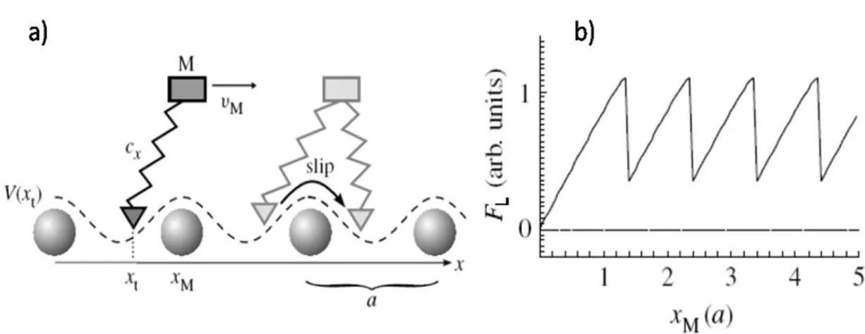
This model is schematically illustrated in Figure 1a taken from the work by Zworner et al. [13].
Figure 1:a) Scheme of the Tomlinson model for a tip sliding on an atomically flat surface, the
tip stick to a potential minimum until the lateral force threshold, necessary to “climb” the potential barrier is reached and then slip to the next minimum. b)The lateral force obtained moving the tip through the periodical potential, note that the signal drop each time the tip reach the new potential minimum [13].
A point-like-tip is elastically attached to a body of mass M, corresponding to the tip base, by a spring of stiffness cx. It interacts with the sample through a periodic potential V(x), where x is the lateral coordinate of the probe, and xt represents the actual position of the tip, while xM represent the position of the tip base M. The tip base moves with a constant velocity vM [14]. The interatomic distance, a, determines the periodic potential V(x).
The lateral force, FL, needed to move the tip in the x-direction, over the periodical potential, can be calculated by:
(
M t)
xL
c
x
x
F
=
−
(11) and is represented in Figure 1b. It is evident that when the tip position corresponds with the cantilever, xt=xM and FL will drop, that means that the energy barrier has been overcome and the tip and the tip base are now alienated, no torsion of the cantilever, no FL. The maximum FL value will correspond to a position that we’ll call xM,jump.and it has been studied that corresponds to xM,jump.=a/4 [12].
The frictional force will be the average value of the lateral force.
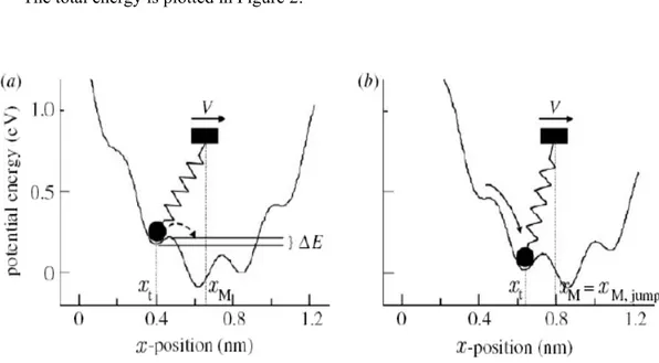
At zero temperature, ignoring the inertia, the total energy of the system, consisting of the potential (V(x)) at the position of the tip and the energy which is stored in the spring, is given by:
( )
1(
)
2 t M x t x total V x c x x E = + − 2 , (12).The total energy is plotted in Figure 2:
Figure 2: Potential diagram of the Tomlinson model at zero temperature. a) The cantilever is
at position xM and the tip is in position xt, trapped in a local minimum and separated from the next minimum by an energy barrier ΔE. b) The cantilever moved further to position xM = xM,jump ,and the tip moved to the new minimum [13].
In Figure 2 the tip is located in correspondence of a minimum, xt, and is separated by a barrier energy ΔE from the next minimum to the right. Since the tip base moves in x direction,
xM will increase and the energy barrier will decrease, see equation 12, until the local minimum vanish, ΔE =0 and the tip moves to the next local minimum.
At finite temperature, thanks to thermal activation, the tip can jump the barrier even if ΔE≠0. The reason is that the tip, at T≠0, oscillates in the potential with a characteristic frequency f0 [12] and will have a probability to jump or not the energy barrier. Gnecco et al.
[15] proposed the following theory starting from this master equation:
) ( ) ( exp ) ( 0 p t t E f t dp ⎟⎟ ⎞ ⎜⎜ ⎛ Δ− − = T k dt ⎝ B ⎠ , (12)
where ΔE is a time function, f0 is the resonant frequency of the tip in it actual minimum and
p(t) represents the probability that the tip does not jump to the next local minimum.
To find the lateral force corresponding to the maximum jump probability, Gnecco et al. proposed a change of variable replacing time by the corresponding lateral force. The resulting master equation is:
)
(
exp
0 L BF
p
dt
T
k
f
dt
=
−
⎜⎜
⎝
−
⎟⎟
⎠
⎜
⎝
⎟
⎠
)
(
)
(
F
LE
t
dF
L 1dp
⎛ Δ
⎞
⎛
⎞
− , (13)This equation can be solved noting that:
v c dx dF dFL L = = dt dx dt x , (14)
where v is the sliding velocity, and assuming that the energy barrier vanishes linearly near the critical point XM,jump with the increasing FL:
( )
F
L(
F
L,jumpF
L)
E
Δ
=
λ
−
, (15)Substituting equations (14) and (15) into equation (13) and following passages better explained in [15], we obtain the final equation:
1 1 0
v
L L Lln
v
F
F
F
=
+
, (16)This logarithmic dependence of friction on velocity, based on thermal activation, can easily be understood as “the more slow you slide the tip more time and more probability the tip has got to jump the energy barrier, the faster you scan the lower the probability will be and so the friction, that is the average value of the FL, will increase”. Of course that this phenomenon can only be explained at atomic or quasi-atomic scales, while at macro-scales the phenomenon is averaged by the large number of contacts and Coulomb-like behaviour is observed.
This dependence ends to exist when the sliding velocity exceeds a critical velocity vc, so that friction becomes independent of velocity. The critical velocity is [12]:
a
c
x2
T
k
f
v
0 B 02
Π
=
, (17)In thepresent work the influence of velocity on the frictional response of the system was also evaluated by performing experiments in the velocity range between 50-1000 nm/s.
1.2 Silicon
Silicon was used as model material throughout all this work.
Nowadays we may say that we’re living in the age of silicon (Si), since it is all around us in term of electronic devices. This is due thanks to its corrosion- and heat-resistance and to its excellent electrical properties [16]. Moreover Si, the element 14, represents one of the cheapest (when 97% pure) and most abundant elements on earth, and it is the second element (after oxygen) in the crust, making up 25.7% of the crust by mass.
It is impressive how strongly the number of published papers with the word “silicon” in the abstract increased during the last decades: approximately 30,000 papers in the 1970s, 84,000 in the 1980s, 135,652 in the 1990s, and in total it has created a database of almost a quarter of a million paper over the last 30 years directly or indirectly written about silicon [17]. Most of these papers focused on technological and experimental aspects of silicon, but these works profoundly influenced the theoretical community. In fact any new theory related to electronic materials is almost always first tested and assessed against the silicon database.
Polycrystalline silicon (poly-Si) has found many applications in integrated circuits. It consists of small crystallites (called grains) separated by thin regions, called grain boundaries. The grain size increases with an increase in the deposition temperature and it depends on the
in-situ (dopants are added during the deposition process) doping concentration. Several advantages are offered by poly-Si: it matches the mechanical properties of single-crystal-Si, it has a good step coverage if deposited by CVD, it has a high melting point, and it can form an adherent oxide [17].
Very pure single-crystal silicon is used for semiconductor applications. On the quantum scale that microprocessors operate on, the presence of grain boundaries would have a significant impact on the functionality of field effect transistors by altering local electrical properties. Therefore, microprocessor fabricators have invested heavily in facilities to produce large single crystals of silicon.
Silicon is the material used to create most integrated circuits used in consumer electronics in the modern world, MEMS/NEMS. Examples of MEMS device applications include inkjet-printer cartridges, accelerometers, miniature robots, microengines, locks, inertial sensors, microtransmissions, micromirrors, micro actuators, optical scanners, fluid pumps, transducers, and chemical, pressure and flow sensors. New applications are emerging as the existing technology is applied to the miniaturization and integration of conventional devices [18].
The high friction force and poor wear behavior of Si represents the limiting factor to a successful operation and the missing reliability of MEMS having parts in relative motion to each other [18]. Micromotors, microgears, and microturbines are examples of MEMS that operate in contact mode (see Figure 3) and friction and wear are their dominant degradation mechanisms.
1.2.1 Crystalline Silicon
Normally Si crystallizes in a diamond structure, forming tetraedrical covalent bonds sp3, on a face-centered cubic (f.c.c.) lattice, with a lattice constant of a
0= 5.43 Å. The basis
of the diamond structure consists of two atoms with coordinates (0,0,0) and a0/4 (1,1,1), see
Figure 4.
The starting material for high purity silicon single-crystals is silica (SiO2). The first step in silicon manufacture is the melting and reduction of silica.
Figure 4: 3D representation of a silicon crystal.
A complex series of reactions actually occur in the furnace at temperatures ranging from 1500°C to 2000ºC. The lumps of silicon obtained from this process are called metallurgical-grade silicon (MG-Si), and its purity is about 98-99% [20]. The next step consists in the purification to the level of semiconductor-grade silicon (SG-Si), which is used as the starting material for single crystalline silicon. The basic concept is that powdered MG-Si reacts with anhydrous HCl to form various chlorosilane compounds. Then the silanes are purified by distillation and chemical vapor deposition (CVD) to form SG- poly-Si [20].
In order to convert poly-Si into one single crystal silicon, there are two main techniques: zone-melting method commonly called the floating zone (FZ) method, and the
Starting from the ingot, the silicon suppliers obtained the wafers, which are thin Si disks (the typical thickness is 0.6-0.7mm). The basic requirements for these wafers are the followings: (i) it has to be very flat to allow the device features to be accurately defined by lithografic methods; (ii) the wafer surfaces should not be contaminated with heavy metal or alkali metal impurities; and (iii) the top surface of the wafer should have a low residual density of lattice defects [22].
1.2.2 Amorphous silicon (a-Si)
Amorphous silicon is the non-crystalline allotropic form of silicon, where the atoms form a continuous random network. Not all the atoms within amorphous silicon are four-fold coordinated. Due to the disordered nature of the material some atoms have a dangling bond which is a defects in the continuous random network, and can cause anomalous electrical behavior.
a-Si is prepared by sputtering or by thermal evaporation; this material has a very high defects density which prevents doping, photoconductivity and the other desiderable characteristics of a useful semiconductor. Electronic measurements were mostly limited to the investigation of conduction through the defect states. In the 1960s, in order to eliminate the defects that prevented a-Si from being useful for electronic devices, a group of researchers had the idea of introducing hydrogen in the sputtering system. The Hydrogenated amorphous silicon (a-Si:H) presented a decrease of the dangling bonds and an increase of the photoconductivity. Hydrogenated amorphous silicon (a-Si:H) has a sufficiently low amount of defects to be used within devices. a-Si:H may be deposited from a gas phase into large area substrates and can be used in flat panel displays based on thin film transistors, or cheap solar cells [23].
The table in the next page presents the properties and the applications of crystalline and amorphous silicon.
In the present work all the experiments were carried out using crystalline Silicon wafers as base material.
Table 1: Crystalline and Amorphous silicon properties and applications [21].
Crystalline Si (c-Si) Amorphous Si (a-Si) Hydrogenated a-Si (a-Si:H)
Structure Diamond cubic.
Short-range order only. On average, each Si covalently bonds with
four Si atoms. Has microvoids and
dangling bonds
Short-range order only. Structure typically contains
10% H. Hydrogen atoms passivate dangling bonds and
relieve strain from bonds.
Typical preparation Czochralski technique, Floating Zone Electronbeam evaporation of Si.
Chemical vapour deposition of silane gas by RF plasma.
Density(g cm-3) 2.33
About 3-10% less
dense. About 1-3% less dense.
Electronic applications Discrete and integrated electronic devices. None
Large-area electronic devices such as solar cells, flat panel
displays, and some photoconductor drums used in
2 Experimental techniques
2.1 AFM
2.1.1 Basic operation principles
Invented in 1982 by Binnig, Quate and Gerber [24], AFM represents a technique of choice for non-destructive, high resolution imaging in many applications areas including biology, material science, electrochemistry, polymer science, data storage, magnetism, and semiconductors. AFM can investigate the conductive and not conductive samples, overcoming in this way the main disadvantage of the previous technologies, such as Scanning Tunnelling Microscope, limited to conductive samples.
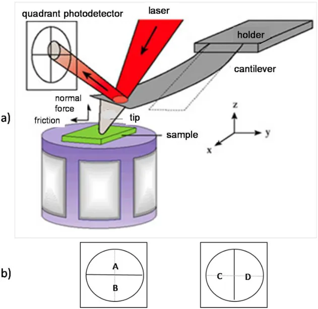
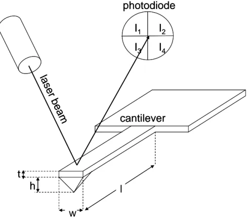
The operation principles of AFM are easy to understand since they’re based on a simple idea: a tip mounted on a micro machined cantilever scans the surface of the samples (Figure 5a, next page) under a constant force, the displacement of the tip, corresponding to the deflection in the normal direction of the cantilever, will give the topographic image of the sample, while the torsion bending of the cantilever will give the lateral force (LF) signal that can be directly correlated to the friction between the tip and the surface. It’s important to remember that in LF images the scan has to be necessarily perpendicular to the longitudinal axis of the cantilever. The deflection Δz, and the normal force F, are controlled by Hook’s law that states: F= Δz•K, where K is the spring constant of the cantilever. Since the force has to be maintained constantly, a feedback system keeps the deflection of the cantilever at the same value. Typical tip radius is about 10 nm, and there are interatomic forces between the tip and the sample.
A piezo element is used to scan the tip line by line across the sample. Both the bending and the torsion of the cantilever are detected by a laser beam focused on the back of the cantilever and reflected towards a position-sensitive photodetector consisting of four-segment photo-detector (Figure 5b). The differences between the signals of the four segments indicate the position of the laser spot on the detector and thus the angular and normal deflections of the cantilever. In particular A-B and C-D signals indicate respectively the normal deflections and the torsion bending of the cantilever.
Figure 5: a) The basic concepts of an AFM working with the laser beam deflection method.
Torsion and bending of the cantilever are measured with the position of the laser beam on the photo diode detector. b) The signal A-B and C-D are respectively a measure of the bending and of the torsion of the cantilever.
The operation principles previously described refer to the contact mode technique in AFM that presents some disadvantages due to the fact that the tip exerts forces to the sample and although these forces are only of the order of 0.1-1 nN, the pressure applied to the sample can easily reach 1000 bar because the contact area is so small. This may lead to structure damage, especially on soft surfaces [25]. There are other options to avoid these disadvantages and these options are dynamic mode and non contact mode AFM [24]. While in contact mode the forces are repulsive (see Figure 8), due to the proximity between the tip and the sample, in non contact mode a stiff cantilever is excited to vibrate near its resonant frequency close to the sample, but not touching i. The cantilever is scanned along the sample and under the
of the cantilever will change and will represent the measurement parameter for the topography of the sample [26].
Figure 6: Diagram of the forces between the tip and the sample. During the approach of the
tip to the surface, first the forces are attractive and then they become repulsive and there is an elastic deformation of the tip and the sample [18].
There is an intermediate regime between the contact and non contact mode and it is called the intermittent or “tapping” mode or semicontact mode. In this case, a stiff cantilever is oscillated closer to the sample than in non contact mode ( see Figure 6). Part of the oscillation extends into the repulsive regime, so the tip intermittently touches or “taps” the surface. The main advantage of this technique is represented by the fact that it is more sensitive to the interaction with the surface, and this gives a possibility to investigate some characteristics of the surface, such as distribution of magnetic and electric domains, elasticity and viscosity of the surface. Furthermore, the force of pressure of the tip on the sample is less than in contact mode and permits to work with softer and easy to damage materials.
In order to obtain quantitative data, the calibration of the bending and the torsion of the cantilever represents a really important issue [14].
2.1.2 Force measurement
Experimentally, the force curve is determined by applying a triangle-wave voltage pattern to the electrodes for the z-axis scanner. This causes the scanner to expand and then contract in the vertical direction, generating relative motion between the cantilever and sample. The deflection of the free end of the cantilever is measured and plotted at many points as the z-axis scanner extends the cantilever towards the surface and then retracts it again. By controlling the amplitude and frequency of the triangle-wave voltage pattern, the researcher can vary the distance and speed that the AFM cantilever tip travels during the force measurement.
From the contact lines of force-displacement curves it is possible to draw information about the elastic-plastic behavior of materials.
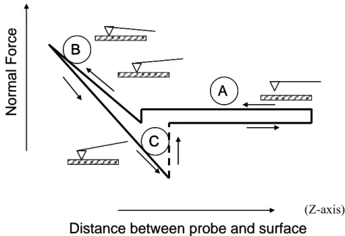
Figure 7, next page, represents a schematic force curve. The approaching and retracting part of the forces are usually different. The reason has to be the fact that the system “cantilever-surface” is not in equilibrium at every distance. In fact close above the surface, the change of the spring elastic force with the distance often cannot counterbalance the corresponding change of attractive surface forces, and equilibrium is lost and the tip “jump in” the sample surface. The onset of this unstable regime is characterized by the point where the gradient of the attractive force exceeds the spring constant [27].
The cantilever starts not touching the surface. In this region, if the cantilever feels a long-range attractive (or repulsive) force it will deflect downwards (or upwards) before making contact with the surface. As the probe tip is brought very close to the surface, it may jump into contact if it feels sufficient attractive force from the sample. Once the tip is in contact with the surface, cantilever deflection will increase as the fixed end of the cantilever is brought closer to the sample. If the cantilever is sufficiently stiff, the probe tip may indent into the surface at this point. In this case, the slope or shape of the contact part of the force curve can provide information about the elasticity of the sample surface. After loading the cantilever to a desired force value, the process is reversed. As the cantilever is withdrawn, adhesion or bonds formed during contact with the surface may cause the cantilever to adhere to the sample some distance past the initial contact point on the approach curve. A key measurement of the AFM force curve is the point at which the adhesion is broken and the cantilever comes free from the surface. This can be used to measure the rupture force required to break the bond or adhesion.
A
B
C
Normal
F
o
rce
Distance between probe and surface
A
B
C
A
A
B
B
C
C
Normal
F
o
rce
Distance between probe and surface
(Z-axis)
Figure 7: Schematic force curve, including approaching and retracting parts. The vertical
axis represents the normal deflection of the cantilever (in V units), which is proportional to the vertical displacement of the laser beam on the photo-detector, while the horizontal axis represents the displacement of the piezoelectric scanner in the Z direction (direction normal to the sample’s surface).Three types of hysteresis can occur: In the zero force line (A), in the contact part (B) and adhesion (C) (adapted [19]).
2.1.3 Calibration
In all AFM force measurements, the AFM cantilever is used to apply forces to the sample under investigation. To extract reliable, quantitative values for material properties from these measurements, the applied forces need to be accurately known, which, in turn, critically depends on reliable and universally applicable force calibration methods for AFM instruments. To obtain quantitative information, the calibration procedure for conversion of measured data to friction forces has to be applied.
2.1.4 Normal Force Calibration
Normal force calibration consists on finding a linear relationship between the normal force and the normal deflection of the tip, measured by the photodiode. The applied force may be calculated from Hooke’s law:
AB
U
βN is the calibration factor and UAB is the signal in the vertical area of the photodiode (see Figure 5b.
The calibration factor is:
K
K
ZM
=
β
, (19)where Kz is the spring constant and K the sensitivity.
The spring constant Kz for bending a cantilever with a rectangular cross section, fixed on one end is:
3
4
3l
Ewt
K
Z=
,
(20).E is the Young modulus, w is the width, t is the equivalent thickness, and l is the length of the cantilever (Figure 8, next page). To account for the tip in the other end, an equivalent thickness t, instead of the real thickness is often calculated from the resonance frequency f0,N :
N f l t 2 0. 2 3 4Π ⋅ ⋅ =
ρ
E 0λ
, (21)Here ρ is the density of the cantilever material and λ0= 0,596864 π.
For other cantilever shapes, kn will be different and more difficult to calculate. The Sensitivity, K, is obtained through the force curve, see
Figure 7, and represents the slope of the curve:
z
U
K
ABΔ
Δ
=
, (22)l
w
h
t
cantilever
photodiode
la
se
r b
e
a
m
I
1I
2I
3I
4l
w
h
t
cantilever
photodiode
la
se
r b
e
a
m
I
1I
2I
3I
4l
w
h
t
cantilever
photodiode
la
se
r b
e
a
m
I
1I
2I
3I
4Figure 8: Schematic diagram of an AFM with a rectangular cantilever.
2.1.5 Lateral Force Calibration
For the lateral force calibration we applied the wedge calibration method, introduced by Ogletree et al. [28] and improved by Varenberg et al.[29], who took into account the adhesion between the sample and the tip as well. Wedge calibration method relies on measuring friction loops as a function of applied load and substrates with two well-defined slopes, for example on flat and sloped surface. It is assumed that the width of the wedge is significantly larger that the tips radius and for this reason this method does not require knowledge of the shape of the tip.
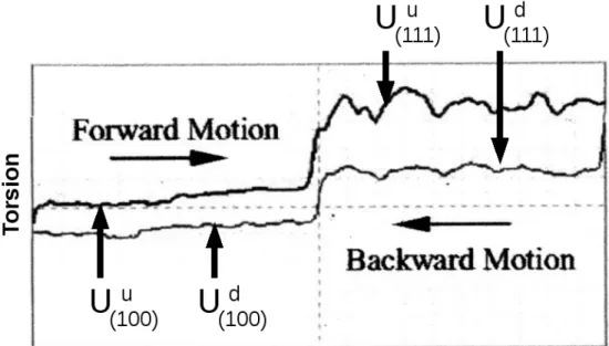
For the calibration of AFM in terms of lateral forces we used a commercially available silicon calibration grating form Mikromash (Figure 9), with exact pitch value of 10 mm and slope angle of 54°448, formed by the (111) and (100) crystallographic planes.
Scanning trace
Scanning trace
Figure 9: SEM images of TGF11 silicon calibration grating from Mikromash, the scanning
trace to perform the calibration is evidenced.
The calibration requires the values of the friction loop obtained by scanning continuously back and forth across one flat and one slope portions of the grating (see Figure 10).
Figure 10: Friction loop corresponding to the scanning trace marked in figure 5.
Lately, we calculate the following values for both the zones, (100) and (111):
2
d u U U
2 d u U U + = Δ , (24)
W represents the half width of friction loop and Δ the friction loop offset.
Investigation of forces acting on the cantilever during the sample scanning leads to the equation:
(
cos)
(
cos)
sin (111) ) 111 ( ) 100 ( ) 111 ( 2 ) 111 ( + ⋅ Θ ⋅ 0 cos sinΘ Θ= ⋅ + Δ − Δ − ⋅ Θ ⋅ ⋅ Θ eff A eff N eff N W F F Fμ
μ
N F N F N F , (25)where Θ stands for the angle of the slope surface, is the applied load, and FA the adhesion force obtained by the force curve.
eff
This equation is not always solvable, for this reason the calibration has to be repeated for different normal loads. The solution of Equation 18 provides, for any given load and adhesion FA, two possible solutions of the friction coefficient m for the slope. The real solution, however, must be smaller than 1/ tgΘ, since otherwise it yields an unreasonable negative calibration factor.
eff
The calibration factor is calculated through the formula:
(
)
) 111 ( ) 111 ( sin cos D C L LU
F
− 2 2 2 ) 111 ( cos 1 W F Feff A N L Θ− Θ Θ ⋅ + =μ
μ
β
, (26)and the effective lateral force can be finally calculated :
=
β
⋅
, (27)2.1.6 Manipulation of Nanoparticles
The idea of nanoparticles manipulation opens new perspectives, for nanotribological friction studies using AFM. In fact, while FFM detects the LFs acting between the sample surface and the AFM tip [30], usually limited to a to a very narrow set of materials (mostly silicon, silicon oxide, silicon nitride and diamond) and to sphere-on-flat type contacts, the manipulation of nanoparticles overcame this limitation and increased the number of possible materials combinations [30].
During the past decade different laboratories published several articles dealing with the subject of NPs manipulation using AFM. Having an overview of these works it becomes clear that there are two main trends: some groups considered dynamic mode suitable to manipulate NPs and others preferred contact mode: the groups of Dietzel and Schirmeisen [30], Yang et
al. [31], Bhushanù et al. [32], Sitti et al. [33] and Yong Ju Yun et al. [34] approach the
manipulation of nanoparticles through the contact mode AFM, while the groups of Ritter et
al. [35, 36] and Paolicelli et al. [37] and Mougin and Gnecco [38] preferred to work in
dynamic mode. Below, the vantages and disadvantages of each method will be reported. Operation of an AFM in dynamic mode, compared to the so-called contact mode, allows the study of fragile sample surfaces and weakly adhering particles without damaging the structures or “cleaning up” the scanned area. This last fact represents one of the main drawbacks of contact mode. In fact, with particles that are weakly bounded to the substrate, the imaging by contact mode, becomes difficult even with very low normal forces close to the “snap off” condition of the cantilever [30], in this way there is a risk of manipulation in an uncontrolled form that is difficult to avoid.
MANIPULATION IN DYNAMIC MODE
In dynamic mode the periodic motion of the cantilever prevents the tip degradation during the lateral scan due to the shear force caused by adhesion, and eliminates the jump-to-contact instability through the restoring force of the cantilever, K•Ao, where K is the cantilever stiffness and Ao the oscillation amplitude [39]. Moreover, one of the main advantages of the non contact AFM (NCAFM) is the flexibility of the process, that can be easily switched between imaging, translation or in plane rotation, marking single nanoparticles and cutting of nanoparticles [35]. On the other hand, while dynamic techniques, based on the so-called amplitude modulation mode of AFM operation, proved to be very successful in air and with small nanoparticles, they failed in the attempt to move bigger (>150nm) NPs, as for example the Sb nanoparticles in the Schirmeisen experiments [30]. This
failure was most likely caused by strong repulsive tip-particle interactions. Such strong interactions are, on the one hand, necessary to ensure sufficient energy transfer for particle manipulation but result, on the other hand, in unstable cantilever oscillations and often even a complete oscillation breakdown [30]. Another disadvantage of the dynamic approach is that it can be measured only the threshold amplitude for particle translation, and, besides the fact that recent theory predicts that this value is proportional to the static friction force of the particle, it still represents an indirect measure for friction.
MANIPULATION IN CONTACT MODE
In contrast, contact mode allows a more straightforward interpretation of the results, as the cantilever torsion during particle dislocation is a direct measure of the pushing force applied to the particles [30] that represents the friction force. In contact mode the most important parameters are the cantilever’s stiffness and the normal force. With stiffer cantilevers, we often observe uncontrolled motion of the particles during regular scans; only cantilevers with adequate stiffness enable well-controlled particle manipulation allowing for the extraction of quantitative values of the particle-substrate friction. Normal force control permit to choose between mode image and manipulation, just choosing a normal force smaller or bigger than the threshold value, if the normal force is far above the dislocation threshold, uncontrolled particle can occur [30]. We can control better the movement of the nanoparticles and avoid the detachments with a soft approach to the nanoparticles [33].
In short: NCAFM is important in term of process flexibility, since it permits to work in image mode and to manipulate even really small and weakly bounded nanoparticles, but the movement cannot be controlled easily and detachments occur. CAFM on the other side is suitable to manipulate a vast range of nanoparticles and gives a direct measure of the friction force, and it permits to work in both imaging and manipulating mode once the threshold force is found.
In this work contact mode AFM was chosen and retained suitable to manipulate the NPs. Dynamic mode was utilized to visualize the area before the manipulation, in order not to interfere with the NPs.
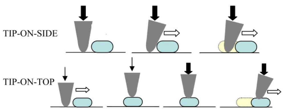
Two different approaches were used: tip-on-side and tip-on-top. Figure 11, next page, illustrates these two basic approaches.
TIP-ON-SIDE
TIP-ON-TOP
Figure 11: Schemes of NPs manipulation experiments. TIP-ON-SIDE, at loads larger than
manipulation threshold, the tip pushes the particle out of its way. TIP-ON-TOP. at loads lower than the manipulation threshold, the tip is positioned upon the NP, then the load is increased and the NP start to move together with the tip.
TIP-ON-SIDE MANIPULATION EXPERIMENTS Tip-on-side (
Figure 11) consists in positioning the tip close to a nanoparticle and then move the nanoparticle in contact mode applying a load larger than the manipulation threshold; the friction force will consist in the difference between the value of the friction force between the tip and the sample before and during the manipulation.
In this work, we used two different AFM software packages: Proscan 1.9 and the MATRIX SPM 2.0 (see next section). Only the second one, used in UHV conditions, allows the tip to move along arbitrary vectors, and so permits the operator to position the tip on the side of the chosen NP and impose the sliding of the tip along the wanted trajectory.
TIP-ON-TOP MANIPULATION EXPERIMENTS
Tip-on-top (Figure 11) method, developed by Dirk Dietzel et a. [40], represents a new way of manipulating. Thanks to the software MATRIX SPM 2.0, the tip is positioned on the top of the NP, once the tip is well located the load is increased to FN=48 nN, in this way the NP will slide together with the tip and the lateral force will represent the friction force between the NP and the surface. After the manipulation another scan was performed in the area to confirm if the particle of interest either moved or stayed stuck.
2.2 SEM–EDX
The scanning electron microscope (SEM) is one of the most versatile instruments available for the examination and analysis of the microstructure morphology and chemical composition characterizations [41].
It has many advantages over traditional microscope: it has a large depth of field, which allows more of a specimen to be in focus at one time and has also much higher resolution, so closely spaced specimens can be magnified at much higher levels. Because the SEM uses electromagnets rather than lenses, the researcher has much more control in the degree of magnification (10-10.000x). All of these advantages, as well as the actual strikingly clear images, make the scanning electron microscope one of the most useful instruments in research today.
The working principles are represented in Figure 12.
A beam of electrons is thermoionically emitted from an electron gun fitted with a tungsten filament and accelerated by a differential of potential (1- 50 kV) that is established between the cathode and the anode. The electron beam follows a vertical path through the microscope, which is held within a vacuum. The electron beam, which typically has an energy ranging from a few hundred eV to 40 keV, travels through electromagnetic fields, condenser lenses and objective lenses, which focus the beam down toward the sample to a spot about 0.4 nm to 5 nm in diameter.
When the primary electron beam interacts with the sample, the electrons lose energy by repeated random scattering and absorption within a teardrop-shaped volume of the specimen known as the interaction volume (Figure 13), which extends from less than 100 nm to around 5 µm into the surface. The size of the interaction volume depends on the electron's landing energy, the atomic number of the specimen and the specimen's density. The energy exchange between the electron beam and the sample results in the reflection of high-energy electrons by elastic scattering, emission of secondary electrons by inelastic scattering and the emission of electromagnetic radiation, each of which can be detected by specialized detectors.
Figure 12: Schematic drawing of the electron and x-ray optics of a combined SEM, adapted
by [33].
Figure 13: Generalized illustration of interaction volumes for various electron-speciment
Secondary electrons (SE) are those electrons which escape from the specimen with energies below about 50 eV [42]. They’re generated by the inelastic collision between the primary electrons and the electrons of the first layer of atoms (on the order of a few nanometers in metals and tens of nanometers in insulators). This small distance allows the fine topographic resolution achieved in the SEM. When they got enough energy, they exit the sample and are detected by the collector [43].
The backscattered electrons (BSE) are generated by elastic collision. Having a large fraction of the incident energy they move on straight trajectories toward the detector. They’re used for imaging in the SEM [42], the surface topography can be imaged at lower magnifications with a better shadow effect than with SE and at high magnification with a worse resolution, due to the larger information volume and exit area [42]. The most important contrast mechanism of BSE is the dependence of the backscattering coefficient on the mean atomic number Z, which allows phases with differences in Z to be recognized [44].
SEM equipment include the Energy Dispersive Spectrometer (EDS) which permits to detect and display most of the X-ray spectrum and so determine the element presents on the surface [42]. The accuracy of the precision and resolution of the analysis depends on the volume of characteristic x-ray production, that is defined by the case where the energy of an electron, E, is just sufficient to produce x-rays requiring energy, Ec.The critical energy, Ec, varies with the x-ray of interest. The characteristic peaks obtained are due to x-rays emitted when ionized atoms return to the ground state [45].
In this work it has been used a SEM Hitachi S2400 (IST, Lisboa, Portugal) and a SEM LEO 1530VP (Institute of Physics at the University of Münster, Germany). The EDS analyses were conducted by Oxford INCA Energy 200.
3 Experimental description
This work is divided in two main parts: experiments conduced in ambient conditions and experiments conduced in a ultra high vacuum (UHV).
In ambient conditions the frictional behaviour of Si was studied and also experiments of manipulation of gold nanoparticles were carried out. UHV AFM experiments were used for nanofrictional studies of silicon-on-silicon and for the manipulation of Sb nanoparticles.
Experimental details are given below.
3.1 Experiences in ambient condition
The experiments in ambient condition were performed in air, at room temperature using the commercial AFM Veeco CP-II, shown in Figure 14. The measuring piezo head has a maximum scan range of 100 µm in x and y-directions and 10 µm in the z-direction. The control software used was Proscan 1.9.
The scanning movement of the piezo scanner in the xy plane is represented in Figure 15, where a fast and a slow (step-by-step) scan direction exist. Besides the PZT scanner which moves the sample (or the tip) in the x, y and z directions, another piezoelectric material can exist in the microscope. This piezo is located in the tip holder and is responsible for the vibration of the AFM cantilever which is used in some of the operational modes (dynamic modes, not used in this work).
Figure 15: Raster pattern scanning movement of the PZT scanners used in the AFM ambient
experiments, in the plane of the material’s surface (X-Y plane). The movement occurs as follows: 1-2-3-4-3-5-6-5-7-… ending point.
The procedure for the experiment in ambient condition will be described in the next paragraphs.
C-Si was used as base material. The C-Si samples used were n-type, <111> orientated silicon from Virginia Semiconductors.
Previous to the NPs deposition the Si surfaces were cleaned. The cleaning procedure used, was a simplification of the standard Radio Corporation American (RCA) clean process [46], consisting in four cleaning steps:
1) Immersion of the sample in a solution of H2O2:H2SO4 for 10 minutes; 2) Dip in a solution of HF:H2O for 30 seconds ;
3) Immersion in H2SO4 for 10 minutes;
4) Dip in the above solution of HF for 30 seconds.
All steps were separated by rinses with deionised water and, after the final rinse, the samples were dried with nitrogen and placed into a vacuum chamber for 2 hours.
The preparation and deposition procedure of the gold NPs has been conducted in the laboratory of Karine Mougin in Mulhouse (CNR-S). The gold NPs were produced by colloidal suspension from an aqueous solution of tetrachloroauric acid hydrate (HAuCl4, 3H2O), the details are described elsewhere [38].
A solution of gold NPs was produced in this way. The sizes of the NPs, as determined from transmission electron microscopy (TEM) images, were around 30-60 nm (Figure 16).
The deposition of he gold NPs was obtained by dipping the samples into the solution for 10 to 20 minutes and drying them with a nitrogen flow.
![Figure 3: MEMS device along with pollen and red cells, in order to compare the dimensions[19]](https://thumb-eu.123doks.com/thumbv2/123dokorg/7527021.106580/23.892.246.652.722.1073/figure-mems-device-pollen-cells-order-compare-dimensions.webp)
![Table 1: Crystalline and Amorphous silicon properties and applications [21].](https://thumb-eu.123doks.com/thumbv2/123dokorg/7527021.106580/26.892.106.794.145.676/table-crystalline-amorphous-silicon-properties-applications.webp)
![Figure 12: Schematic drawing of the electron and x-ray optics of a combined SEM, adapted by [33]](https://thumb-eu.123doks.com/thumbv2/123dokorg/7527021.106580/40.892.223.674.124.614/figure-schematic-drawing-electron-optics-combined-sem-adapted.webp)
