2
Contents
1 Introduction 5
1.1 Solar Energy ... 5
1.2 c-Si Solar Cells ... 6
1.3 Efficiency limit ... 7
1.4 Evolution of c-Si solar cells ... 7
1.5 Novel Strategies to improve conversion Efficiency ... 9
1.6 Advanced Solar Cells ... 10
1.7 Solar Cell Numerical Simulations ... 13
1.8 Aim of the Thesis ... 14
2 Modelling of Crystalline Silicon 17 2.1 Numerical Simulations ... 17
2.2 c-Si Models and Properties ... 22
3 Numerical Simulation of the Impact of Design Parameters on the Perfor-mance of IBC Solar Cell 30 3.1 Simulation Approach ... 31
3.2 Results and discussion ... 33
3.3 Conclusions ... 48
4 Understanding the impact of front-side texturing and doping on the performance of c-Si IBC solar cells 50 4.1 Introduction ... 51 4.2 Experimental ... 53 4.3 Modeling Approach ... 55 4.4 Results ………...63 4.5 Discussion ... 83 4.6 Conclusions ... 92
3
5 Modelling of Passivated Contacts 94
5.1 Introduction ... 94
5.2 Simulation approach ... 96
5.3 Validation ... 97
5.4 Results and Discussion ... 98
5.5 Conclusions ... 112 6 Conclusions 116 7 Bibliography 120 Summary 134 Sommario 136 List of Publications 138 Acknowledgments 140
5
One
1 Introduction
1.1 Solar Energy
Solar energy potentially is by far the more abundant energy resource. Even if we consider only emerged continents, its potential energy amount is around 23000 TWy/y [1]. Such value overpass by several orders of magnitude the current world energy consumption of 18TWy [2] and 27TWy projected to 2040. However, around 80% of world energy consumption comes from fi-nite energy resources as coal, fuel and nuclear [2], even when their consump-tion is associated to the so called greenhouse gases. Among these, consider-ing the plenty of potential energy comconsider-ing from sunlight make this option as the most attractive to face a promising future of human society. Even more, solar energy is free, and worldwide accessible. Therefore, it is crucial that in the near future, solar energy will become a very important option in the gen-eration of electrical energy by means of photovoltaic (PV) conversion inside a semiconductor device (solar cells). Among that, according to ITRPV report [3], in 2016 the PV module production capacity of 60GWp is overpassing the global market demand for second consecutive year. Thus, to keep the prices reduction has become the main challenge to PV industry. However, to address this situation, some strategies can be developed by optimizing
mate-6 rials use and by improving conversion efficiency of the PV module/solar cell.
1.2 c-Si Solar Cells
Crystalline silicon (c-Si) solar cells dominates current PV market thanks to the material abundance, low processing cost and relatively high conversion efficiency [3]. In fact, c-Si solar cells industry is associated to integrated cir-cuit market and are the more efficient of commercial solar cells. Moreover, recently, bulk production of c-Si ingots has been also improved on last years by reducing the presence of impurities in crystalline structure, expanding the potential achievable efficiency. However, c-Si characteristics are not the best for PV applications. In particular, c-Si has an indirect bandgap of 1.12 eV equivalent to 1160nm spectrum wavelength cut-off [4] that corresponds to a relatively low absorption coefficient that can be counterposed by using light-trapping schemes. Light-light-trapping consists on the formation of texturized sur-faces covered by Anti-Reflect Coatings (ARC) in front and Back-Reflectors (BR) on rear side in order to catch more efficiently sun light.
To control and avoid the presence of minority carriers at defective interfaces passivation schemes are used. Such passivation strategies are chemical when depositing thin layers of dielectric with charges that catch the interface crys-tal dangling bounds, or electrical when using highly doped regions or depos-iting charged layers to repel the charges from silicon boundaries. According-ly, to collect generated carriers inside the bulk into the metallic contacts, similar structures are needed, but in this case, they have to allow the transport of one type of charges (electrons or holes) and repealing the others from interfaces.
7 1.3 Efficiency limit
Considering only radiative recombination mechanism, Shockley and Queisser [5] estimated a theoretical conversion efficiency limit of 33.5%. However, due to the fact that silicon has an indirect bangap, the radiative re-combination is minimized, but Auger rere-combination becomes dominant. Consequently, on the basis of state-of-the-art semi empirical Auger recombi-nation model [6], Richter et al estimated the limit of efficiency for c_Si in 29.4% [7]. This limit is not feasible, but mark the direction on the task to reach more efficient solar cells. A more realistic or practical limit was pro-posed by Swanson [8] on 26%, but this limit underestimate the potential to apply novel structures as passivated contacts. Considering such structure the practical limit could be considered to 27% keeping same assumptions than Swanson.
1.4 Evolution of c-Si solar cells
The evolution of c-Si solar cells in the history it is summarized on Figure 1.1 and it is clear the increasing trend in the time. Such evolution has been well reported by Green in [9].
8
Figure 1.1: History of c-Si solar cells efficiency. Mono-junction structures are showed in red and hetero-junction in blue. The plot is based on data from NREL report [10]
However, in order to summarize it, the following milestone are presented: In 1941, Ohl reported the first silicon solar cell with an efficiency
around 1% [11]
In 1953, 1954 and 1955 Bell Laboratories announced 4.5% [12], 6% and 10% efficiency [13]
In 1961, commercial cell reported 14.5% efficiency for n-type bulk. In 1963, it was assessed the effect of n-type and p-type bulk in space
radiation, giving a better result for p-type bulks [14]
In 1970 and 1974 Comsat Laboratories reported a 13.7% and 15 % [15]respectively efficiency on p-type silico solar cells
In 1976, Rittner reported an efficiency of 16.7% [16] In 1983, UNSW cell showed 18% efficiency [17]
9 In 1985, UNSW reported for first a 20% efficiency passivated emitter
solar cell (PESC)
In 1988, UNSW announced a fabricated PESC solar cell 21.4% In 1988, Standford, reported a fabricated 22.3% efficiency solar cell In 1989, UNSW fabricated 23% efficiency passivated emitter rear
lo-cally diffused (PERL) solar cell that was improved to 24.7% in 1999. In 2014, Sunpower announced an interdigitated back-contact (IBC)
solar cell of 25% efficiency
In 2016, Kaneka apply HIT junction IBC achieving 26.3% efficiency [18].
1.5 Novel Strategies to improve conversion Efficiency
1.5.1 Selective diffusions and Localized contacts
Doping impurities diffusion are used in contact regions to attract collecting carriers to the metal contact. Similarly, such diffusion is used to avoid that minority carriers arrive to defective interfaces. It has been also demonstrated that doping underneath the metallic interfaces has to be high enough in order to improve interface resistivity and increase the fill factor (FF). However, highly doped regions leads to low resistivity regions, but at the same time in-crease Auger recombination. Such compromise has aimed to reduce metallic interfaces as well than highly doped regions. In fact, beyond that fabrication process are increased, localized contacts with selective diffusion increased efficiency when modeling these structures [19].
10 1.5.2 Passivated Contacts/Selective contacts
To achieve a good passivation on c-Si is one of the keys to achieve higher efficiencies. Indeed, metallized interfaces are highly defective and they can be passivated and collect carriers thanks to the use of passivated contacts. Such structure consists on applying a very thin layer of a wide bandgap ma-terial (usually SiO2) between metal and silicon interface forming heterojunc-tions (HJT). Collection and transport mechanism are achieved thanks to the quantum tunneling mechanisms occurring through the passivating layer. The efficiency improvements of this architecture are expressed on reported effi-ciencies over 25% [20][21], with the potential to go beyond.
1.6 Advanced Solar Cells
Recently, in the task for efficiency increase and cost reduce of solar cells, new cell designs have been proposed and developed. In this way, novel con-cepts has been presented to attract the interest of the PV industry.
1.6.1 Heterojunctions solar cells
In order to achieve a better passivation and at the same time carrier collec-tion, as previously explained, a junction from 2 different materials are used. This material is applied as a thin layer among silicon and metal (See Figure 1.2). This thin layer has to accomplish two passivating conditions: chemical and electrical passivation by using ionized dopants to achieve a good band alignment. This concept commonly consider the deposition of amorphous silicon (a-Si) layer, and has demonstrate clear improvements especially on
11 open circuit voltage (Voc) values. In fact, world record c-Si solar cell achieved 25.6% of conversion efficiency with a Voc of 0.74 V.
Figure 1.2: HIT Solar Cell [22]
1.6.2 Tunneling Oxide Passivated Contact (TOPcon)
This novel concept created by Fraunhover ISE, consist on the use of the ad-vantages of conventional homo-junction solar cell as light-trapping and a complete rear passivated contact (see Figure 1.3). Therefore, transport among the solar cell is simplified because the straight carrier collecting paths and using high quality passivation schemes. Such advantages are expressed in terms of FF and Voc improvement that have been demonstrated to reach 83.2% FF, 0.718 V of Voc with 25.1% of efficiency. However, front contact width has to be as small as possible in order to avoid shading losses.
12
Figure 1.3: Sketch of TOPcon solar cell [20][23]
1.6.3 Interdigitated Back-Contact IBC
Back-Contact Back-Junction solar cells (BC-BJ) allow improving conver-sion efficiency (η) because of the absence of front contact shadowing and simplified cell interconnection at module level (see Figure 1.4). Thanks to these advantages, efficiencies over 25% have been already reported [21][18] with the potential to go beyond. On the other hand, BC-BJ efficiency is sen-sitive to recombination mechanisms related to fabrication process, such as SRH recombination due to defectiveness in bulk and at interfaces [24].
13 1.7 Solar Cell Numerical Simulations
Advanced solar cells are becoming more complex and usually demands more fabrication process steps and thus, requiring the assist of simulation tools. Accordingly, the use of numerical simulations has become a strategic and critical key in the improvement of PV efficiency by optimizing their geomet-rical and process design. Moreover, simulation tools provides an insight of Physics inside the solar cell and assist researchers to predict efficiency de-pendence from design parameters [26]. It is worth noting, that due to their own inherent complexity, advanced solar cell structures can be only investi-gated using two or three dimensional simulations tools.
Numerical simulators, so called technology computer-aided design (TCAD), are a very used tool in the semiconductor industry and have been developed for more than 20 years [27]. Therefore, TCAD support has been stablished as strategic target to achieve nowadays photovoltaics challenges: more efficient and less costly advanced solar cells. In general, device simulations consist on the solution of the semiconductor transport equations in semiconductor re-gions using metal contacts as boundary conditions. Even more, solutions ac-count several external conditions such as interaction of impurities, doping, traps defects, activation energy, tunneling, etc. Because of their unique opto-electrical physics, solar cells simulations have to account a wide range of pa-rameters that include optical and electrical models according to properties of materials composing the device especially anti-reflect coating (ARC), and their interfaces.
14 1.8 Aim of the Thesis
The aim of this Thesis is to provide guidelines for the design of c-Si based solar cells featuring advanced architecture and novel physical mechanisms as interdigitated back contact back junction (iBC) structures and carrier selec-tive contacts. Accordingly, this contribution is based on TCAD simulations (Sentaurus) and is focused on identifying critical design parameters by un-derstanding the competitive mechanisms associated to each design parame-ter. Thereby, by accounting technological constrains, optimized designs are presented in the path to achieve the highest efficiency.
In order to present such contribution, this thesis is presented in different chapters.
In Chapter 2, the general state-of-the-art properties related to c-Si solar cells is described. In particular, c-Si models and parameters are identified and pre-sented with the aim to calibrate and implement them in TCAD Sentaurus platform to obtain realistic results.
In Chapter 3, a theoretical study based on electro-optical numerical simula-tions of the impact of geometrical and doping parameters on main figures of merit of crystalline silicon back-contact back-junction solar cells is present-ed. The studied design parameters are the doping level in front surface field (FSF), back surface field (BSF) and emitter, and the main geometrical pa-rameters. A doping level value that allows the maximization of the efficiency for the three highly doped regions can be clearly identified. In particular, for BSF and emitter, an efficiency degradation is observed for relatively lower doping values and is ascribed to the higher contact recombination while for higher doping values the Auger recombination plays a significant role in re-ducing the ultimate efficiency. In FSF region the recombination due to de-fects at the front interface is the main limiting mechanisms for efficiency. On
15 the basis of the analysis, a marked sensitivity of the efficiency to the gap and pitch size is caused by the series resistance increase. The efficiency exhibits a maximum value for an emitter coverage fraction (R) of 85%. However, in the case of lower emitter coverage, Auger, Shockley-Read-Hall (SRH): in bulk and at interfaces are detrimental for the cell conversion efficiency. In Chapter 4, a novel IBC simulation model is presented, validated and de-ployed to study optical light-trapping and front recombination competitive mechanisms. In collaboration with TUDelft, the model presented on Chapter 2 has been upgraded and calibrated. A more accurate simulation methodolo-gy is presented to account in detail the optical and passivation mechanisms of front texturization. Its validation has been carried out with respect to a novel homo-junction IBC c-Si solar cell based on ion implantation and epi-taxial growth, comparing measured and simulated Reflectance (R), Trans-mittance (T), Internal Quantum Efficiency (IQE), External Quantum Effi-ciency (EQE) spectra and current density-voltage characteristics. As a result of the calibration process, the opto-electrical losses of the investigated de-vice have been identified quantitatively and qualitatively. Then, an optimiza-tion study about the optimal front surface field (FSF) doping, front-side tex-turing morphology, and rear-side geometry has been performed. Simulation results show that a not-smoothed pyramid-textured front interface and an op-timal FSF doping are mandatory to minimize both the optical and the recom-bination losses in the considered IBC cell and, consequently, to maximize the conversion efficiency. Similarly, it has been showed that recombination losses are affected more by the doping profile rather than the surface smoothing. Moreover, the performed investigation reveals that the optimal FSF doping is almost independent from the front texturing morphology and FSF passivation quality. According to this result, it has been demonstrated that an IBC cell featuring an optimal FSF doping does not exhibit a
signifi-16 cant efficiency improvement when the FSF passivation quality strongly im-proves, proving that IBC cell designs based on low-doped FSF require a very outstanding passivation quality to be competitive. Deploying an optimization algorithm, the adoption of an optimized rear-side geometry can potentially lead to an efficiency improvement of about 1%abs as compared to the refer-ence IBC solar cell. Further, by improving both emitter and c-Si bulk quali-ty, a 22.84% efficient solar cell for 280-μm thick c-Si bulk was simulated. In Chapter 5, a validated simulation model is used to identify critical design parameters when using passivated contacts in a conventional solar cells. Simulation results shows that energy barrier, electron and holes tunneling masses, and oxide thickness are the critical parameters that constrains transport mechanisms. With the aim to study effects related to band align-ment it has been deployed a set of simulations for different band gap and electron affinity range. It has been demonstrated that transport mechanism are limited also for band alignment quality which is correlated to the calcu-lated build in voltage (Vbi). For small Vbi values, transport mechanism are
constrained by the absence of holes on c-Si/oxide interface. For large Vbi
values, transport mechanisms are constrained by the band bending achieved on oxide/deposited layer interface. It was also qualitatively identified a Vbi
interval in which a good transport mechanisms are achievable for optimal band alignment cases. Regarding small Vbi values, it is identified the assist
of in-diffusion in c-Si in order to improve solve aforementioned transport is-sues. Similarly, a critical doping that allows tunneling mechanisms work is also identified and it depends on to the density of filled states and relative permittivity of deposited material.
17
Two
2 Modelling of Crystalline Silicon
In this chapter, a review of the solar cell modeling is presented. It is consid-ered state-of-the-art crystalline silicon parameters as well than new models. Accordingly, it is explained the adoption of a novel model describing intrin-sic recombination for silicon. Finally, the typical solar cell simulation scheme is described.
2.1 Numerical Simulations
Numerical simulations are based on the discretization of a virtual device into Finite Elements that reproduces numerically electrical behaviour of semi-conductor devices. For the case of solar cell devices, the simulator estimates charge distribution and transport mechanisms according to the so called Drift Diffusion Model. Therefore, the solar cell device are replicated virtually by means of geometrical, materials stack, interfaces and doping profiles discre-tized onto a grid so called mesh [28] and then solved calculating electrical parameters according to boundary and physical conditions.
18 The accuracy of the numerical solution of the device is related to the grid resolution but, at the same time a large number of points could be limited by computational resources. Consequently, discretization of the device is a cru-cial stage on device modelling, because it has to lead to an accurate solution in feasible computational time. However, solar cells are highly symmetrical devices that allows to account the most element of symmetry to consider as simulation domain. Therefore, by modelling only this simulation domain, the entire solar cell behaviour can be replicated. However some special consid-erations have to account in particular regions of the solar cell in which pa-rameters gradient is large among spatial reference. Hence, a small mesh step size has to be considered in such regions. According to Altermatt et al [29] a good mesh can be achieved by starting with a resolution of parallel to 1nm from the front interfaces and 10nm for other cases and the mesh step size can be coarser going inside the cell. However, such initial mesh resolution value is a reference that can be modified depending on the mechanisms that domi-nates some regions. For instance, these regions are i) front surface, where the absorption of most energetic photons occurs and surface recombination needs to be modelled accurately, ii) back surface, again for optimal model-ling of surface recombination, both on passivation layer and contacts, iii) the interface region between emitter and base. Similarly, to reproduce accurately light-trapping mechanisms different resolution are recommendable similarly to mimic tunnelling mechanisms in case of passivating contacts, and of course, considering the grid size (i.e. 2D or 3D simulation). Thus, choosing an adequate mesh is an iterative process that account accuracy and attainable computational time for solving the parameters of the device.
19 In order to accurate reproduce semiconductor modelling for different condi-tions, the Drift Diffusion model is applied to attain an adequate accuracy in modelling of solar cells [29]. Then, the semiconductor are solved by cou-pling Poisson equation (1) with continuity equation (2 and 3) and Drift-Diffusion equations (4 and 5):
∇2Φ(𝑟, 𝑡) = −𝜌(𝑟,𝑡) 𝜀 (1) 1 𝑞∇ ∙ 𝐽⃗⃗⃗ 𝑝 = 𝐺𝑂𝑃𝑇− 𝑅𝑝− 𝜕𝑝 𝜕𝑡 (2) 1 𝑞∇ ∙ 𝐽⃗⃗⃗ 𝑛 = 𝑅𝑛−𝐺𝑂𝑃𝑇+ 𝜕𝑛 𝜕𝑡 (3) 𝐽𝑝 ⃗⃗⃗ = −𝑞𝜇 𝑝𝑝𝐸−𝑞𝐷𝑝∇𝑝 (4) 𝐽𝑛 ⃗⃗⃗ = −𝑞𝜇 𝑛𝑛𝐸+𝑞𝐷𝑛∇𝑛 (5) 2.1.3 Optical Modelling
Beyond that there is several methods to solve the optical behaviour of a solar cell by calculating optical generation GOPT, Ray-traycing algorithm is the
most commonly used due to the low use of computational resources and the capability of reproduce texturing effects when evaluating light-trapping. Therefore, in this thesis we have used Ray-tracer from Sentaurus [28] in the optical platform.
Commonly, a 3-D optical simulations are performed by raytracing simu-lator accounting for a thin film stack boundary condition to model ARC at the front interface and elemental texturing element at top. The incidence an-gle of rays is passed as input to a Transfer Matrix Method (TMM) solver
20 which returns the reflectance, transmittance, and absorbance to the raytracer assuming absorbance, refractive and extinction coefficients as probability within Monte Carlo approach [28],[30], [31]. The angle of refraction is cal-culated by the raytracer according to Snell’s law.
In particular, the TMM-based model adopted for the ARC stack layers uses a 2x2 matrix for each interface between two materials, thus representing the relationship between the incoming and outgoing transmitted and reflected waves provided at each interface as follows:
(𝑇𝑗 + 𝑅𝑗+) = 𝑀𝑗,𝑗+1( 𝑇𝑗+1− 𝑅𝑗+1− ) (6) 𝑀𝑗,𝑗+1 = [𝐴 𝐵 𝐵 𝐴] (7) where
C=exp(2πinjdj/λcosj) and D=exp(-2πinjdj/ λcosj)
j is the material index and j is the incidence angle in the material j. The
re-lationship for thin layers with a thickness d smaller than the coherence length of the light becomes:
(𝑇𝑗 − 𝑅𝑗−) = 𝑀𝑗( 𝑇𝑗+ 𝑅𝑗+) (8) 𝑀𝑗 = [𝐶0 𝐷0] (9) where
C=exp(2πinjdj/λcosj) and D=exp(-2πinjdj/ λcosj).
Assuming that the transmitted wave at the end of the ARC stack is not back-reflected and knowing the intensity I and the angle of incidence of the in-put light, it is possible to relate the layers of the ARC stack through the fol-lowing relationship:
21 (𝐼 0) = 𝑀𝐴𝑅𝐶 ∗ (𝑅𝐴𝑅𝐶 𝑇𝐴𝑅𝐶) (10) where M*
ARC is the inverse matrix given by the product of all interfaces
ma-trices, RARC and TARC are the reflectance and the transmittance of the ARC
layer, respectively. Hence, the computational cost of solving the optical problem is clearly reduced and simplified. However, this assumption is valid before until the second reflectance becomes apparent, such effect will be dis-cussed on Chapter 4.
As result of the optical model, the 3-D optical generation map calculated is spatially integrated over the distance from the front interface in order to cal-culate the 1-D optical generation profiles. Lastly, the optical generation map is interpolated on the spatially nonuniform 2-D mesh for the device simula-tion [32].
2.1.4 Boundary conditions
In order to mimic the symmetry of the simulation domain and to describe some electrical scenarios, boundary condition has to be carefully specified and designated. For instance, in optical simulation, the boundaries between symmetry elements in optical simulation has to be set with perfect reflectivi-ty to account properly the behaviour of the complete solar cell. In case of emulating ARC effects, TMM boundary conditions has to be specified, as well as Snell’s law in the other cases. Accordingly, for electrical simulation, the boundary condition has to be specified on the metallic contact in order to model the conditions in which the solar cell has to be evaluated (i.e. different voltages to build J-V curve). It is worth noting that, for electrical simulation, on the boundaries of simulation domain, current and charges are assumed to
22 be symmetrical, then, there is no charge crossing from one symmetry ele-ment to another.
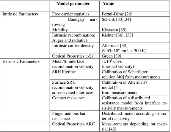
2.2 c-Si Models and Properties
c-Si dominates PV market because the low costs achieved thanks to research and development contribute by electronic field.
Table 1 Summary of the physical models and parameters used in modelling c-Si solar cells.
Model parameter Value
Intrinsic Parameters Free carrier statistics Fermi-Dirac [26] Bandgap
nar-rowing
Schenk [33][34] Mobility Klaassen [35] Intrinsic recombination:
Auger and radiative
Richter [36], [37] Intrinsic carrier density Altermatt [38]
(9.65×109 cm-3 at 300 K)
Optical Properties c-Si Green [39] Extrinsic Parameters Metal/Si interface
recombination velocity
1x107 cm/s
(thermal velocity) SRH lifetime Calibration of Scharfetter
relation [40] from measurements Surface SRH recombination velocity at passivated interfaces Calibration of Altermatt's model [41] from measurements Contact resistance Calibration of a distributed
resistance model from interface re-sistivity measurements
Finger and bus bar resistance
Distributed model according to ma-terial resistivity
Optical Properties ARC Measurements depending on mate-rial [42]
Consequently, parameters from c-Si have been reported and studied deeply and have been assumed for PV community to deploy theoretical studies. Due
23 to its inherent simplicity, solar cell can be considered as diode with a high quality emitter working on low injection regime from electronic point of view [29]. Therefore, parameters and models used on PV field has to de-scribe accurately such behaviour and has been studied and reported by Al-termatt et al [29] and Fell et al [26] and summarized on Table 1. It is worth noting that models and parameters described are directly related on the pre-viously explained Drift Diffusion model. In general, parameters can be con-sidered intrinsic, those implicitly realated to the material (c-Si) and extrinsic, those related to fabrication process.
Most of the detailed models are already implemented in TCAD Sentaurus. However, it was not the case of intrinsic recombination semi-empirical mod-el proposed by Richter et al [6]. In this case, the modmod-el was implemented by means of Physical Model Interface in Sentaurus [28]. Such model was vali-dated according to experimental data reported [6] and showed on Figure 1 and Figure 2. Effective lifetime has been estimated by:
1 𝜏𝑒𝑓𝑓 = 1 𝜏𝑖𝑛𝑡+ 1 𝜏𝑠𝑟ℎ+ 1 𝜏𝑠 (11)
Where 𝜏eff is the effective lifetime measured from
Quasi-Steady-State-Photoconductance (QSSP) method [43], 𝜏int is lifetime factor reported on [6],
and 𝜏SRH and 𝜏s is used as fitting parameter to estimate bulk lifetime and
24
Figure 1: Implemented Auger model validated by [6]
25 Intrinsic physical models are implemented according to state-of-the-art, while the extrinsic physical models are implemented by calibration or meas-ured parameters.
Accordingly, recombination losses due to trap-assisted recombination through deep defect level and due to defects at material interfaces are com-monly modelled by assuming the single-level trap model by Shockley-Read-Hall (SRH) [44], [40] with traps in the energy mid-gap. In this way, bulk lifetime (τsrh) is calculated by the doping dependant model according to:
𝜏𝑆𝑅𝐻= 𝜏𝑚𝑎𝑥 1+(𝑁𝐴,𝐷
𝑁𝑟𝑒𝑓)
𝛾 (12)
where 𝜏max are related to the value estimated by using fabrication param-eter fitted in (𝜏eff equation), NA,D represents the acceptor or donor doping
concentration, respectively. In order to evaluate doping process related is-sues for solar cell fabrication, Nref and γ are used as calibration parameters to
model the SRH recombination lifetime in the different doped regions of the simulated solar cell. Similarly, to account for SRH recombination due to de-fects at material interfaces are modelled by surface recombination velocity that usually is estimated from measurements by fitting 𝜏𝑆𝑅𝐻= 𝜏𝑚𝑎𝑥
1+(𝑁𝐴,𝐷
𝑁𝑟𝑒𝑓) 𝛾
(12. It is worth noting that some works has reported a dependence of SRV with doping concentration at interface [14], [18]. In order to model the very highly defective metal/semiconductor interface, almost thermal surface recombination velocity is usually assumed to 1x107cm/s.
26
Figure 3: Simulation process scheme
The optical generation rate profiles is calculated assuming illumination with normal incidence with respect to the device plane and standard AM1.5G spectrum (1000 W/m2) [47]. Then the electrical simulation is de-ployed in order to reach solar cell FOM and spectral response, as it is ex-plained on Figure 3.
Accordingly, simulation-based works have employed a two-step simula-tion approach [26]. First, an optical model, typically based on ray tracing (RT) or rigorous Maxwell's solvers for devices with nano-textured features, derives the generation profile of electron-hole pairs within the device. Sec-ond, an electrical model based on drift-diffusion uses as an input the calcu-lated optical generation profile [26]. For the sake of simplicity, this approach typically involves in each step the use of different simulation domains. In
27 fact, the optical simulation is carried out on an element that features textured surfaces (light-trapping) with the aim of properly accounting for the optical situation within the silicon. The electrical simulation instead usually is set up on an approximated simulation domain that simply features planar surfaces.
30
Three
3 Numerical Simulation of the Impact of
Design Parameters on the
Perfor-mance of IBC Solar Cell
In this Chapter, updated physical models of realistic parameters were used on TCAD simulations in order to present a systematic and extensive analysis of the dependence of monocrystalline silicon BC-BJ solar cell FOM on the doping level of the different regions and on main geometrical parameters. The aim of this paper is twofold. One aim is to deepen our physical under-standing of BC-BJ solar cells. The second one is to provide guidelines for the design of BC-BJ solar cells. To this purpose, it has been used the simula-tion results about different physical mechanisms, such as the recombinasimula-tion of photogenerated carriers and the influence of doping levels and geomet-rical parameters on electgeomet-rical field intensity and parasitic resistance. Nu-merical Simulation of the Impact of Design Parameters on the Performance of Back-Contact Back-Junction Solar Cell.
(This Chapter is based on the following publication: P. Procel, M. Zanuccoli, V. Macca-ronio, F. Crupi, G. Cocorullo, P. Magnone, and C. Fiegna, “Numerical simulation of the impact of design parameters on the performance of back-contact back-junction solar cell,” J. Comput. Electron., vol. 15, no. 1, pp. 260–268, Mar. 2016.)
31 3.1 Simulation Approach
Figure 1 reports a schematic representation of the element of symmetry of the simulated solar cells. It has been considered a FZ-Si n-type doped wafer featuring a resistivity of 2 Ω-cm within the range reported by McIntosh et al. [48]. The doping profiles in BSF, FSF and emitter are described by Gaussian functions featuring a peak located at the edge of the interface and with a junction depth of 2µm for BSF and emitter and of 1µm for FSF region [49].
Figure 1: Element of symmetry of BC-BJ solar cell used as domain of simulation
3-D optical simulations have been performed by raytracing simulator ac-counting for a thin film stack boundary condition to model ARC at the front interface. The incidence angle of rays is passed as input to a Transfer Matrix Method (TMM) solver which returns the reflectance, transmittance, and ab-sorbance to the raytracer. The angle of refraction is calculated by the ray-tracer according to Snell’s law. The front surface is coated by a double-layer anti-reflective coating (ARC) composed by 42nm Si3N4 and 27nm SiO2, texturized by regular upright pyramids featuring a 10 µm-wide base and opening angle between the two faces of the pyramid equal to 70 degrees. Such ARC configuration is close to the optimum one.
32 The non-metallized back side is passivized by a 0.1 µm-thick SiO2 layer, thus, bottom internal reflectance is calculated by means of Fresnel equations according to the kind of back interface, passivated or contacted by alumi-num. The 3-D optical generation map calculated for different wafer thick-ness values is spatially integrated over the distance from the front interface in order to calculate the 1-D optical generation profiles. Lastly, the optical generation map is interpolated on the spatially nonuniform 2-D mesh for the device simulation.
The Drift-diffusion model, suitable to attain an adequate accuracy in model-ing of solar cells, has been applied by means of numerical simulations by fi-nite element simulator Sentaurus TCAD. As explained in Chaper 2, Physical models have been calibrated by means of state-of-the-art parameterizations [28] and material properties have been considered to calculate realistic val-ues of FOM. Recombination losses due to trap-assisted recombination through deep defect level has been modelled by assuming the single-level trap model by Shockley-Read-Hall (SRH) [44],[50] with traps in the energy mid-gap. To account for SRH recombination due to defects at material inter-faces (either textured and planar), we used the doping dependent models of surface recombination velocity, at passivated interfaces suggested by Glunz et al. [51] with the parameterization reported in [41], consistently with the adopted ni value. It has been considered a 100 µm-wide metal ohmic contact without potential barrier and resistivity of 2 mΩ∙cm2. The recombination
ve-locity for carriers at metal/Si interfaces has been set to 1x106 cm/s. The opti-cal generation rate profiles has been opti-calculated assuming illumination with normal incidence with respect to the device plane and standard AM1.5G spectrum (1000 W/m2) [47]. Lastly, we have assume fully ionized and acti-vated doping concentrations in our simulations.
33 3.2 Results and discussion
In order to investigate the impact of the main doping and geometrical param-eters of BC-BJ solar cell over FOM, we have performed simulations by changing doping peaks in emitter, FSF and BSF regions, and then geomet-rical parameters. In each set of simulations, we changed only one parameter at time in order to study its impact on the BC-BJ performance. All simula-tions were carried out under illumination to estimate Jsc recombination losses
and in dark conditions [52] to evaluate the impact of the recombination loss-es on Voc [53].
3.2.1 Doping Analysis
We simulated the entire space of parameters obtained by varying the doping peak concentration of FSF from 2.31x1015cm-3 up to 1.44x1022cm-3, of BSF
and emitter from 1x1018cm-3 up to 5x1022cm-3 range. We have considered a
pitch of 955 µm, a 5 µm-wide gap and 200 µm-thick wafer. The maximum efficiency equal to 22.3% was obtained for doping peak concentrations equal to 3.47x1018cm-3, 1.44x1020cm-3 and 4.16x1019cm-3 for FSF, BSF and
emit-ter, respectively. We observed, within the investigated doping concentration range, that in each region (BSF, FSF and emitter), a change in doping level does not affect appreciably the recombination and the carrier transport of the other regions of the device [54]. For this reason, in the following we will discuss separately about the impact of the doping of each region on FOM.
34
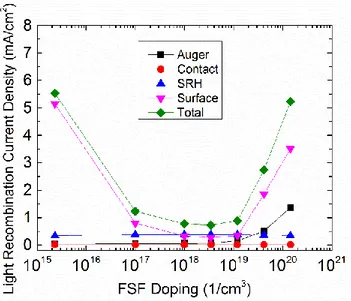
Figure 2 Simulated BC-BJ solar cell FOM as a function of FSF doping peak concentration (Cfsf).
Ef-ficiency exhibits a bell-shape with a clear maximum value at doping concentration level of 3x1018 cm
-3. J
sc and Voc exhibit qualitatively the same trend
3.2.1.1 FSF Doping
Figure 2 shows solar cell FOM trends for different doping peak concentra-tion of FSF diffusion (Cfsf,pk). We observe that η exhibits a bell-shaped
lead-ing to a maximum value for Cfsf,pk of 3.48 x1018 cm-3 confirming qualitative
trends reported by King et al. [55]. The η trend follows the Jsc bell shape,
which is explained by the presence of a minimum of the of the total recom-bination current density under illumination for short-circuit conditions (see Figure 3).
35
Figure 3 Recombination losses components under illumination in short-circuit conditions explaining Jsc. behavior that dominates the efficiency trend in FSF doping peak concentra-tion (Cfsf) experiment. Total recombination (green) minimum point matches with maximum η
in Figure 2
In turn, the trend of the total recombination current density is dictated by the trap-assisted recombination at the Si/SiO2 front interface. For low doping
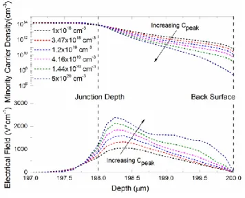
levels (before the efficiency peak), the rate of the SRH recombination due to surface defects at the front texture interface decreases with decreasing dop-ing level. As a matter of fact, a reduction in minority carrier density in the FSF region is caused by the relatively higher electrical field intensity as Fig-ure 4 shows.
36
Figure 4 Comparison of minority carrier (hole) density and electrical field intensity for dif-ferent FSF doping peak concentration at short-circuit condition under illumination in FSF region. Higher FSF doping levels lead to stronger electrical field intensity in the junction depth and to lower minority carrier density values at interface. Depth equal to 0 um indi-cates the front interface position
At high doping levels (beyond the efficiency peak), the SRH surface recom-bination rate becomes stronger again due to the higher SRV doping depend-ent value at interface contrasting with the concdepend-entration of minority carriers. An additional but less relevant contribution to the increase of the total re-combination at high Cfsf,pk is due to the Auger recombination, which clearly
increases as a function of doping. It is worth noting that FF increases due to reduction of series resistance, as reported in [56].
3.2.1.2 BSF Doping
As shown in Figure 5, by increasing the peak doping concentration of BSF (Cbsf,pk), η initially rises and afterwards slightly decreases leading to a value
37 that maximizes η for (Cbsf,pk = 1.44 x1020 cm-3). Similarly to the FSF region,
the influence of doping level on η is dictated by the Jsc trend, which is
ex-plained by the mirrored curve of the total recombination current density un-der illumination for short-circuit conditions (see Figure 6).
Figure 5. Simulated BC-BJ solar cell FOM as a function of BSF doping peak concentration (Cbsf). Efficiency exhibits a maximum value for peak doping concentration level 1.44x1020 cm-3. Jsc and Voc exhibit similar trends
By increasing the doping level, a lowering of the recombination at base con-tact is observed, hence leading to an increase of JSC and η. This is ascribed to
the a reduction of the minority carrier density at the Si/Al interface thanks to the stronger electrical field intensity with increasing Cbsf,pk (Figure 7).
38
Figure 6 Recombination losses contributions under illumination in short-circuit conditions explaining Jsc. behavior that dominates η trend in BSF doping peak concentration (Cbsf)
ex-periment. Auger recombination (black squares) exhibits an increase for higher Cbsf leading
to a minimum point in Total recombination (green). A trade-off between recombination losses at contact and Auger recombination mechanism occurs
Figure 7. Comparison of minority carrier (hole) density and electrical field intensity for dif-ferent BSF doping peak concentration at short-circuit condition under illumination in the BSF region. Higher doping levels lead to stronger electrical field intensity in the junction depth and to lower minority carrier density values at Si/Al interface
39 However, for relatively higher doping levels, the slight increase of the total recombination is due to the rise of the Auger recombination, which clearly depends on doping. Then, a trade-off, allowing to maximize η, is achieved for intermediate doping levels.
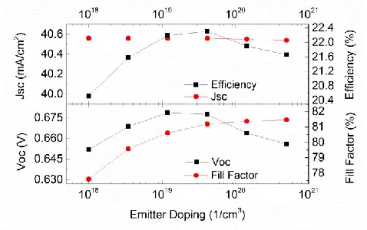
3.2.1.3 Emitter Doping
Figure 8, showing FOM trends for different doping peak concentration of the emitter diffusion (Cem,pk), indicates remarkable variations of Voc, FF and
consequently of η. We observe that η exhibits a bell shape leading to a max-imum for a Cem,pk value of 4.16x1019 cm-3.
Figure 8. Simulated BC-BJ solar cell FOM as a function of emitter doping peak Ce.
Effi-ciency exhibits a clear maximum value at peak doping concentration of 4.19x1019 cm-3. V oc
follows the same trend. However, the maximum point for η is different from Voc due to the
degradation of FF for lower Ce values
The trend of Voc becomes apparent by examining the mirrored behaviour of
40
Figure 9. Saturation current competitive components in dark scenario. The bell shape ex-hibits a clear minimum point at doping peak concentration, Cem,pk=1.2x1019 cm-3 explained
in terms of contact and auger recombination trade-off in dark. SRH contribution increase is not appreciable considering scale size
On the one hand, an increase in Cem,pk leads to a degradation of contribution
of recombination at emitter contact in agreement with King [55]. This is as-cribed to the stronger electrical field intensity at Si/Al interface for higher Cem,pk that results into a reduction of minority carrier density at contact
inter-face as Figure 10 confirms for open-circuit conditions under illumination. On the other hand, for higher Cem,pk, Auger recombination contribution
41
Figure 10. Comparison of electron density and electrical field intensity for different emitter doping peak concentrations in open-circuit condition under illumination in emitter region. Higher doping levels lead to stronger electrical field intensity in the junction depth and to lower minority carrier density values at Si/Al interface
A trade-off between the contact recombination and the Auger recombination leads to a minimum of the dark recombination current density for Cem,pk =
1.2x1019 cm-3, close to the value reported in [57]. It is worth noting that the Cem,pk value observed for maximum η is higher due to the FF contribution.
Indeed, FF increases with increasing Cem,pk due to a reduction of the emitter
sheet resistance. The highest calculated efficiency η is 22.3%. The marked difference from 24.2% [57] can be mainly ascribed to longer minority carrier lifetime, and higher passivation quality of silicon interfaces.
3.2.2 Geometry Parameters Analysis
In this section, we performed an extensive analysis of the influence of geo-metrical design parameters on the performance of the BC-BJ solar cell. The
42 geometrical considered parameters are: gap between emitter and BSF, BSF width (Wbsf), emitter width (We), and pitch (as defined in Figure 1). We
con-sidered the doping peak concentrations calculated in section 3.1, allowing to maximize η.
3.2.2.1 Gap and BSF Width
We performed simulations by changing the BSF region width Wbsf (Figure
1) and gap width at the same time, keeping constant the pitch (1000μm) and We (725μm). The assumed gap surface recombination velocity for carriers
(SRV) is 25cm/s for base doping concentration according to [41].
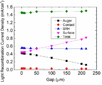
Figure 11 shows that η decreases with increasing gap width, due to the markable reduction of FF. Evidently, the effect of the gap variation is re-flected in a BSF and gap resistivity trade-off that explains the FF degradation for longer gap.
Figure 11. Simulated BC-BJ solar cell FOM as a function of gap. Efficiency and FF exhibit decreasing trend with increasing gap width.
43 However, we notice that Jsc has a negligible dependence on gap width. In
fact, as Figure 12 shows, by changing the gap longitude there is a rise in SRH surface recombination rate contribution due to the absence of apprecia-ble electrical field intensity at rear interface for wider gaps. In this case, the decrease in auger recombination loss is ascribed to wider gap, which leads to a smaller volume of highly doped BSF diffused region. Similarly, the in-crease in Voc can be explained, but in this case, Auger recombination
degra-dation becomes slightly more significant than surface recombination contri-bution.
Figure 12. Recombination losses components under illumination in short-circuit condition explaining Jsc and Voc trends. Auger recombination (black) exhibits a degradation that is
compensated by surface defect recombination rise.
On the other hand, the trap-assisted recombination at the gap surface in-creases because of the absence of the electrical field (which prevents the high carrier density at the BSF interface). Evidently, the effects of surface defectiveness in rear interface expressed in terms of surface recombination velocity become critical for the gap region in agreement with reports in
44 [58],[59]: for relatively high defective interfaces, it is expected that surface defect recombination component becomes significant causing the degrada-tion of Jsc and Voc. In any case, a longer gap causes an efficiency
degrada-tion due to resistive and recombinadegrada-tion losses confirming what observed in [60],[61].
3.2.2.2 Emitter Width
We performed simulations by changing the emitter width We (Fig.1) and that
of the BSF region (Wbsf) at the same time, keeping the pitch constant
(1000μm) as well as the gap width (5μm). In Figure 13, we plot FOM as a function of the We to pitch ratio (R). According to our hypotheses, a higher
value of R implies both an increase of We and a decrease of Wbsf. We
ob-served an increasing trend of η as R increases up to a value of 0.85, while a slight η reduction is observed for higher R values. Evidently, η enhancement is explained by Jsc rising trend[62] while η decrease by FF degradation. As
Figure 14 shows, the decreasing trend of the total recombination under illu-mination for short-circuit conditions is mainly dictated by Auger and SRH recombination reduction at higher R, due to the higher value of Cbsf,pk with
45
Figure 13. Simulated BC-BJ solar cell FOM as a function of emitter/pitch ratio (R). η exhib-its slight a bell shape with a maximum value of 0.85. For lower ratio the trend follows Jsc,
while for higher values FF degradation becomes prominent
Figure 14. Recombination losses components under illumination in short-circuit scenario explaining Jsc trend as a function of emitter coverage ratio (R). R increasing means a
gen-eral degradation of recombination contributors ascribed to electrical shadow effect reduc-tion for larger emitters [49]
46 The observed FF degradation at higher R is ascribed to the higher emitter re-sistivity (ρem = 42.76Ω/□) with respect to the BSF resistivity (ρbsf = 9.67Ω/□).
Therefore, a maximum η value at R of 0.85 is calculated. It is worth noting that, because the optimum R value depends on lateral transport resistance, it is influenced by bulk resistivity, emitter and BSF sheet resistance and there-fore on the doping levels. This dependence explains the different R values reported in literature [63],[59].
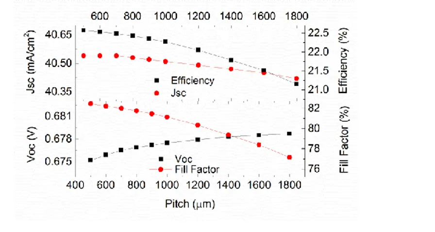
3.2.2.3 Pitch
In order to understand the impact of the pitch over BC-BJ performance, we performed a set of simulations changing the pitch, keeping constant the emit-ter to pitch ratio (0.85) and the gap (5 μm). Figure 15 illustrates that η de-creases with increasing pitch, mainly due to the FF lowering. Hence, an in-crease of the pitch causes a rise of series resistance because of the wider dis-tance between contacts [64].
Figure 15. Simulated BC-BJ solar cell FOM as a function of pitch for an emitter coverage ratio of 0.85. η decreases as pitch length increases following FF trend. Jsc exhibits a
47 The minimum simulated pitch size is 500μm, since lower pitch values would imply Wbsf smaller than the BSF contact size. Therefore, due to this design
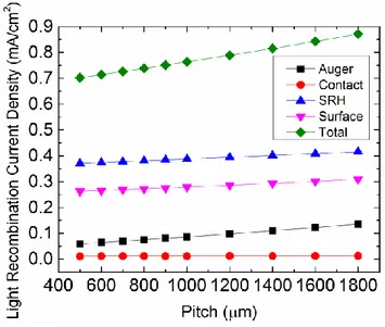
constraint, the minimum simulated pitch can be considered as the maximum efficiency pitch reported in [63],[59],[65]. It is worth noting that all recom-bination current density contributions increase with the pitch value, as shown in Figure 16. This is ascribed to the wider area affected by electrical shading [62]. The observed trend explains the slight decrease in Jsc illustrated in
Fig-ure 15. It is worth noting that in all experiments, contact size is assumed to be constant while the pitch changes. This means that contact recombination contribution is lower for larger pitches. While the impact on Jsc is negligible
(less than 3% contact recombination contribution for optimum Cbsf on Figure
6), that on Voc is more marked (around 20% contact recombination
contri-bution for optimum Ce on Figure 9).
Figure 16. Recombination losses components under illumination in short-circuit scenario explaining Jsc. For the same emitter coverage ratio, R=0.85, recombination losses are
48 3.3 Conclusions
In this Chapter, It has been performed performed an extensive study of the impact of geometrical and doping parameters of BC-BJ solar cells on the main figures of merit, by means of a wide set of numerical simulations. The results reveal that the efficiency curve as a function of doping exhibits a bell shape with a clearly identifiable maximum value for the three regions (BSF, FSF and emitter). The efficiency degradation for lower doping values is explained in terms of higher contact recombination for BSF and emitter, and in terms of higher SRH surface recombination for FSF. The efficiency decrease observed at higher doping values is explained in terms of higher Auger recombination for BSF and emitter, and in terms of SRH surface re-combination losses for FSF. For the simulated solar cell, the values of peak doping that maximize η are: 4.16x1019 cm-3 for emitter, 1.44x1020 cm-3 for
BSF and 3.48x1018 cm-3 for FSF.
Additionally, we observed efficiency degradation as a result of wider gap re-gion, due to the resistive losses and the SRH surface recombination losses in this region. The maximum efficiency as a function of emitter/pitch ratio R is obtained for R=0.85. The efficiency decrease for smaller R is explained in terms of higher recombination losses (Auger and SRH recombination) in electrical shadowed regions, due to the reduced p-n junction electrical field intensity, which causes a higher minority carriers density. The efficiency de-crease for higher R is ascribed to larger resistive losses in the emitter region compared to BSF. Finally, we also observed efficiency degradation for larger pitch values, due to the FF decrease caused by the increase of the resistive losses.
50
Four
4 Understanding the impact of front-side
texturing and doping on the
perfor-mance of c-Si IBC solar cells
In this Chapter, a TCAD-based simulation platform has been developed to account accurately and in detail the optical and passivation mechanisms of front texturization. Its validation has been carried out with respect to a novel homo-junction IBC c-Si solar cell based on ion implantation and epitaxial growth, comparing measured and simulated R, T, IQE, EQE spectra and current density-voltage characteristics. As a result of the calibration pro-cess, the opto-electrical losses of the investigated device have been identified quantitatively and qualitatively. Then, an optimization study about the opti-mal front surface field (FSF) doping, front-side texturing morphology, and rear-side geometry has been performed. The proposed simulation platform can be potentially deployed to model other solar cell architectures than ho-mo-junction IBC devices (e.g. passivated emitter rear cell, passivated emitter rear locally diffused cell, hetero-IBC cell) Simulation results show that a not-smoothed pyramid-textured front interface and an optimal FSF doping are mandatory to minimize both the optical and the recombination losses in the considered IBC cell and, consequently, to maximize the conversion
effi-51
ciency. Similarly, it has been showed that recombination losses are affected more by the doping profile rather than the surface smoothing. Moreover, the performed investigation reveals that the optimal FSF doping is almost inde-pendent from the front texturing morphology and FSF passivation quality. According to this result, it has been demonstrated that an IBC cell featuring an optimal FSF doping does not exhibit a significant efficiency improvement when the FSF passivation quality strongly improves, proving that IBC cell designs based on low-doped FSF require a very outstanding passivation quality to be competitive. Deploying an optimization algorithm, the adoption of an optimized rear-side geometry can potentially lead to an efficiency im-provement of about 1%abs as compared to the reference IBC solar cell. Fur-ther, by improving both emitter and c-Si bulk quality, a 22.84% efficient so-lar cell for 280-μm thick c-Si bulk was simulated.
4.1 Introduction
As it was noted in Chapter 1, both the front and the rear side still represent significant sources of optical and electrical losses even in IBC solar cells. To this purpose, PV research community is focusing on the study of innovative technological solutions aimed to minimize these losses. Concerning the front side, different texturization techniques, anti-reflective coatings (ARCs) dep-ositions and front surface field (FSF) formation processes have been pro-posed to reduce both optical and recombination losses. As matter of fact, the analysis of novel texturing processes in high-efficiency solar cells has been elucidated [66]–[71]. On one hand, in fact, some papers have shown clear improvements in case of pyramid-textured or nano-textured structures main-ly due to a reduction of front-side optical losses [66], [68], [69]. On the other
52 hand, some works have highlighted potential improvements in case of smoothed texturization due to a significant reduction of front-side recombi-nation losses [70], [71]. This reveals the existence of a trade-off between two competitive mechanisms, such as the recombination at front side and the light management. In addition, other contributions have discussed the opti-mization of the FSF in IBC solar cells in terms of recombination losses, lat-eral resistance losses and UV-light stability [72][56]. Concerning the rear side of IBC solar cells, the analysis and the optimization in terms of rear ge-ometry and process parameters is typically done by means of numerical sim-ulations, which aid cell design and fabrication through a detailed loss analy-sis [49], [63], [73]–[77]. Commonly, most of simulation-based works have employed a two-step simulation approach [26], [78]. First, an optical model, typically based on ray tracing (RT) or rigorous Maxwell's solvers for devices with nano-textured features, derives the generation profile of electron-hole pairs within the device. Second, an electrical model based on drift-diffusion uses as an input the calculated optical generation profile [26], [78]. For the sake of simplicity, this approach typically involves in each step the use of different simulation domains. In fact, the optical simulation is carried out on an element that features textured surfaces with the aim of properly account-ing for the optical situation within the silicon. The electrical simulation in-stead usually is set up on an approximated simulation domain that simply features planar surfaces. Obviously, the usage of different simulation do-mains requires the adoption of some correctives with the aim of properly im-porting the calculated optical generation profile in the equivalent planar elec-trical domain accounting for the effect of texturing also in the elecelec-trical model [26]. In fact, such simulation methodology leads to a loss of accuracy when evaluating in detail optical and electrical mechanisms of the FSF.
53 In this Chapter, we present a detailed TCAD-based opto-electrical model de-veloped for the study and the optimization of a fabricated reference IBC c-Si solar cell. Differently from the abovementioned two-step modelling ap-proach, our simulation framework involves a two-dimensional (2-D) geo-metrical model that includes the exact modeling of a pseudo-random pyra-mids front texturing morphology both in the optical and electrical simula-tions. As a consequence, our modelling approach allows directly and proper-ly accounting for the optical effect of textured front side, transport and re-combination mechanisms, without the need to approximate the optical gen-eration profile under an equivalent planar simulation domain and to use cor-rection factors in the considered physical models [26].
The developed opto-electrical device model has been firstly calibrated and validated with respect to a fabricated reference IBC solar cell. Reflectance (R), transmittance (T), internal quantum efficiency (IQE), external quantum efficiency (EQE) and electrical measurements have been used for the cali-bration process. Therefore, a detailed analysis of the opto-electrical losses has been realized for the reference device. Then, the calibrated device model has been deployed to perform an extensive simulation study of the impact of different FSF doping levels and front-side texturing morphologies on the IBC solar cell performance. Such an investigation has been also carried out by considering different front surface passivation qualities. Finally, the de-veloped device model has been used to optimize the rear-side geometry of the reference IBC solar cell.
54 Reference IBC solar cell was based on FZ n-type c-Si wafer, 280-µm thick and resistivity of 2.5 Ωcm. Such device fabricated through a novel self-aligned process which combines phosphorous ion implantation for the FSF and the back surface field (BSF), and epitaxial growth of the boron-doped emitter [79][80]. The front side of our solar cell consists of a textured inter-face with random pyramids, while the rear side is planar (Figure.1). Both in-terfaces are covered by thermally-grown SiO2 and plasma-enhanced
chemi-cal vapour deposited SiNx layers in the double role of passivation stack and
ARC. Metallic contacts are realized by evaporated 2-um thick Al fingers, opportunely placed in the middle of the emitter and of the BSF (see Section 4.3 for details on geometry). Two 3×3 cm2 solar cell samples were
fabricat-ed: the first one features a FSF (FSF sample), exhibiting a sheet resistance equal to 250 Ω/□, while the second is not endowed with the FSF (NO-FSF sample). At the rear side of these devices, the gap between the BSF and the emitter was self-defined during the process and is around ~1.5 µm. Defining pitch the distance between the starting points of two consecutive emitters, the two solar cell samples featured a 1-mm wide rear pitch.
The morphological analysis of the front textured interface was performed by means of Scanning Electron Microscopy (SEM, Philips XL-50) and Atomic Force Microscopy (AFM, NT-MDT nTegra NT-MDT) pictures with the aim of extracting the statistical distribution of the height and overlap of the random pyramids. Wavelength-dependent R and T were measured by a Perkin Elmer Lambda 950 spectrophotometer in the wavelength range between 300 and 1200 nm. Thickness, refractive indexes and extinction coefficients of SiO2 and
SiNx ARC layers were extracted by means of a J. A. Woollam spectroscopic
ellipsometer. Current density-voltage (J-V) measurements were performed with a continuous class AAA Wacom solar sun simulator, while EQE
meas-55 urements were extracted through an in-house built setup that includes a New-port monochromatic illuminator. Quasi steady-state photo-conductance tech-nique was used to evaluate the effective minority carrier lifetime. The phos-phorus implanted and boron epitaxial grown doping profiles were extracted from electrochemical capacitance (ECV) measurements. The contact re-sistance of the related aluminium-coated BSF or emitter layers, deposited on
c-Si FZ wafers of opposite polarity, was measured by means of Transmission
Line Method (TLM).
4.3 Modeling Approach
The modelling approach adopted in this work involves the usage of the same simulation domain, whose 2-D cross-section is shown in Figure.1. In particular, we simulate both optically and electrically a front texturing based on pseudo-random pyramids with the aim of accurately preserving the in-formation related to its effect on light management, passivation and carriers transport. Our modelling approach requires a more extended simulation do-main for the optical simulation and a finer mesh in the front textured mor-phology for electrical simulation as compared to the equivalent flat structure. Nevertheless, several advantages by far counterbalance the slightly greater computational effort: (i) the more accurate distribution of the photo-generated electron-hole pairs within the device, (ii) the proper modelling of the free-carrier absorption, and (iii) the better representation of transport and recombination mechanisms occurring at the textured front side of the solar cell. Based on the proposed approach and according to the geometrical and physical parameters of the reference IBC solar cell, we deployed a numerical
56 TCAD simulator [28] for running our developed opto-electrical device mod-el.
4.3.1 Modelling of solar cell geometry and doping concentration pro-files
The geometrical model used in the optical and electrical simulations has been developed according to the features of the reference IBC solar cell. The illustration of the considered 2-D simulation domain, representing the small-est element of symmetry of the reference cell, is reported in Figure.1. The width of the simulation domain has been set to the half of the rear pitch (i.e. 500 µm). As the BSF-to-pitch ratio is 20%, the emitter width and the BSF width have been set to 400 µm and 100 µm, respectively. As a result of the previously mentioned process [80]¡Error! No se encuentra el origen de la referencia.[79], based on isotropic etching of the silicon, the gap between the emitter and the BSF has been modelled with an arc of circumference having a radius of 1.5 µm. Air/cell front interface is texturized by random pyramids, while cell/air rear interface is flat. Both interfaces are covered by SiO2/SiNx ARC stack.
57
Figure.1: 2-D cross-section of the considered simulation domain (dimensions are not to scale). 0.0 0.2 0.4 0.6 0.8 1.0 1.2 1.4 1015 1016 1017 1018 1019 1020 1021 D opi ng C once nt rat ion ( cm -3 ) Depth (m) SIMS BSF BSF model SIMS FSF FSF model SIMS Emitter Emitter model
58
Figure.2: ECV-based and modeled doping concentration profiles. For BSF and FSF doping profiles cerf functions are used. For emitter doping profile, 3x1019 cm-3 is kept constant
within 0.2 and 0.85 µm and gaussian functions describe doping concentration changes near emitter boundaries.
To properly simulate the mechanisms related to highly doped regions such as BSF, FSF and emitter, the corresponding doping concentration profiles have been modeled by analytical functions according to ECV measurements, as shown in Figure.2. The FSF, BSF and emitter regions were found to be 0.6-µm, 0.8-µm and 1.4-µm deep, respectively. In case of FSF, a complementary error function (cerf) was deployed with diffusion depth and surface concen-tration parameters set to 0.2 µm and 2 x 1019 cm-3, respectively. For BSF doping profile, a superposition of two cerf was used with parameters 0.04 µm and 2 x 1020 cm-3 for the first cerf and 0.3 µm and 4 x 1019 cm-3 for the second. Differently, for the doping profile of the emitter, we mimicked the nature of doping profile of the epitaxial grown layer: a constant doping value within the deposited thickness was set to 3 x 1019 cm-3 while the boron
in-version layer at the surface and the diffusion tail in the bulk were modelled with two independent gaussian profiles, whose peak values (again 3 x 10¹⁹
cm-3) were positioned at a depth of 0.2 µm and 0.85 µm, respectively. The
front texturing has been modelled by a sequence of triangles with a fixed base angle of 54.7°, which is related to the adopted wet-alkaline etching process. It is worth noting that the statistical distributions of triangles' height and overlap were extracted from measured AFM images, as shown in Figure.3 for the height distribution. Then, the extracted statistical distributions have been fitted through analytical probability distribution functions, as the skewed normal dis-tribution function reported in Figure.3.
![Figure 1.2: HIT Solar Cell [22]](https://thumb-eu.123doks.com/thumbv2/123dokorg/2875994.9852/11.748.103.658.108.386/figure-hit-solar-cell.webp)
![Figure 1.3: Sketch of TOPcon solar cell [20][23]](https://thumb-eu.123doks.com/thumbv2/123dokorg/2875994.9852/12.748.215.642.107.335/figure-sketch-topcon-solar-cell.webp)
![Figure 2: Implemented Auger model validated with measurements reported in [6]](https://thumb-eu.123doks.com/thumbv2/123dokorg/2875994.9852/24.748.192.540.583.932/figure-implemented-auger-model-validated-measurements-reported.webp)