Coulomb blockade directional coupler
P. Pingue,a兲 V. Piazza, and F. Beltram
NEST-INFM & Scuola Normale Superiore, I-56126 Pisa, Italy I. Farrer, D. A. Ritchie, and M. Pepper
Cavendish Laboratory, University of Cambridge, Madingley Road, Cambridge CB3 0HE, United Kingdom
共Received 7 October 2004; accepted 16 December 2004; published online 26 January 2005兲 A tunable directional coupler based on Coulomb blockade effect is presented. Two electron waveguides are coupled by a quantum dot to an injector waveguide. Electron confinement is obtained by surface Schottky gates on a single GaAs/ AlGaAs heterojunction. Magneto-electrical measurements down to 350 mK are presented and large transconductance oscillations are reported on both outputs up to 4.2 K. Experimental results are interpreted in terms of Coulomb blockade effect and the relevance of the present design strategy for the implementation of an electronic multiplexer is underlined. © 2005 American Institute of Physics. 关DOI: 10.1063/1.1857078兴
Controlled directional injection of electrons from one electronic waveguide to another is being intensively investi-gated owing to its importance in wavelength multiplexing and in telecommunication routing devices. While photonic multiplexers represent a mature technology, electronic steer-ing devices are still at their infancy.
Pioneering designs were demonstrated exploiting a field-effect tunable barrier between two semiconductor waveguides,1–5implementing a Y-branch switch or switching the electrons by means of electric side-gates.6–8 An elec-tronic device based on two electron waveguides coupled by an open interaction window rather than a tunneling barrier was also proposed9–11and realized,12but so far no switching behavior has been demonstrated in this configuration.
In this letter we describe a scheme where the coupling element between two semiconductor waveguides is a single quantum dot 共QD兲 and Coulomb blockade 共CB兲 governs electron routing. We shall demonstrate that in the classic configuration with two electron waveguides mixing at an open ballistic window a QD can be induced—with appropri-ate biasing conditions and geometry—and employed as a gate-controlled coupling element between the two waveguides.
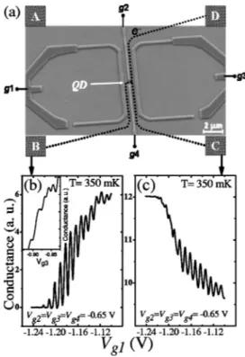
Figure 1共a兲 shows a scanning electron microscope 共SEM兲 picture of the device. Schottky gates are labeled g1– g4. The Al split-gate structure was nanofabricated by e-beam lithography and thermal evaporation. The waveguides of the device described in this work have a total length L = 7.5m each and a geometrical width W = 0.44m. The central split-gate is w = 0.17m wide while the coupling window is l = 0.57m long. The GaAs/ AlGaAs heterostruc-ture contains a two-dimensional electron gas共2DEG兲 located 70 nm below the surface with a mobility of = 3.7 ⫻105cm2/ V s and a carrier concentration of n = 2.4
⫻1011cm−2 at 350 mK.
In our experiment gates g2–g4 were negatively biased by a dc voltage共Vg2, Vg3, Vg4, respectively兲, while gate g1 共bi-ased Vg1兲 was employed as a plunger gate. A drain-source ac voltage共VDS= 100V兲 was applied at the input waveguide
共Ohmic contact D in Fig. 1兲.
The ac current flowing through outputs B and C was measured by two current preamplifiers and phase-locked techniques. A lower ac excitation of 20V was also used to test that the device was in the linear regime also at the lowest temperatures.
Panel共b兲 and 共c兲 in Fig. 1 show the differential conduc-tance measurements relative to collectors B and C, respec-tively, when an ac bias is applied to contact D. The Ohmic-contact A was left floating. Biasing Vg2, Vg3, and Vg4 at −0.65 V, high-contrast oscillations in the output current ap-pear on both collector waveguides at 350 mK as a function of Vg1in the range from −1.24 to − 1.1 V. One of the outputs
共Fig. 1, c兲 displays a 5%-wide current modulation while the
a兲
Electronic mail: [email protected]
FIG. 1.共a兲 SEM picture of the coupled-waveguide device. Schottky gates are labeled as g1–g4. Letters A to D represent the Ohmic contacts 共not shown兲; 共b兲 differential conductance in the collector B 共through the QD兲, and 共c兲 corresponding conductance in the collector C. Inset: “symmetric dot” conductance as a function of Vg3.
APPLIED PHYSICS LETTERS 86, 052102共2005兲
0003-6951/2005/86共5兲/052102/3/$22.50 86, 052102-1 © 2005 American Institute of Physics
other collector共Fig. 1, b兲 shows a 100%-wide current modu-lation oscilmodu-lation in the output current.
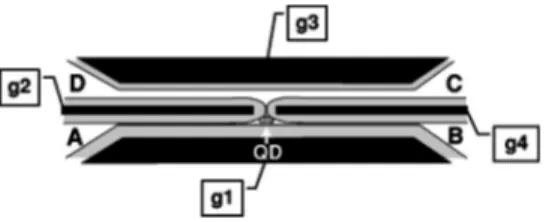
This behavior can be explained taking into account the formation of a QD in the CB regime in the region indicated by the black disk in the schematic sketch shown in Fig. 2. The QD presence in that position was verified in all cool-downs, and a specific characterization of each waveguide was performed in order to exclude the presence of uninten-tional dots in the input or output channels.13,14By symmetri-cally reversing the biasing configuration of gate electrodes a dot symmetrically located in the opposite of the coupling region could be induced. This dot was indeed observed when contact B was employed as emitter and A and D as collector waveguides共A, D兲. In the case of the device shown here it yielded a lower contrast in conductance measurements 关see inset in Fig. 1共b兲兴. We attribute this behavior to a different coupling regime to the reservoir, probably related to the tun-nel barrier of the output chantun-nel.
The CB-oscillation pattern obtained by measuring the current from contacts B and C showed aphase shift, ex-cluding the possibility that the QD extends to the whole cen-tral region and demonstrating the switching behavior of our device.
Figure 2 shows a scheme of our device: gate-depleted regions in the 2DEG are indicated by gray areas. It is quite intuitive that a confined dot can be created when the cou-pling window is pinched-off and when the bottom waveguide is almost closed. Tunnel barriers originate from small grains or lithographic imperfections in the metallic gates that in-duce a constriction between the QD and the adjacent waveguides.
In the following, a low-temperature study of the magne-totransport properties of the dot represented in the scheme of Fig. 2 is reported. CB characterization was performed as a function of source-drain bias 共VSD兲 and as a function of a
magnetic field parallel to the 2DEG plane, in order to mini-mize orbital magnetic-coupling effects. Figure 3共a兲 shows
the well-known Coulomb diamonds in the QD conductance as a function of VSDand Vg1. The height共in the VSD
direc-tion兲 of the diamonds can be used to measure the charging energy UCBbetween two adjacent electron levels.
15
From the maximum Coulomb gap UCB= e2/ C
tot⯝1.6 meV a total dot capacitance of Ctot⯝100 aF is deduced.
In a simple model of an ungated 2D disk-shaped QD the total capacitance is given by Ctot= 4⑀0⑀rD, where D is the
QD diameter, and⑀r= 12.5 is the dielectric constant of GaAs.
From the measured value of Ctot= 100 aF we derive a dot diameter of D = 0.23m, in good agreement with the geom-etry of our device. From this diameter and the charge density of electrons in the original 2DEG, we estimate that there are ⬃100 electrons in the dot under the operating conditions of Fig. 3, left.
The mean periodicity of the Coulomb oscillations re-ported in Fig. 1⌬Vg1= e / Cg1= 9.4 mV corresponds to a gate capacitance of Cg1= 17 aF giving, therefore, = Cg1/ Ctot = 0.17 as “lever arm” value between the applied gate voltage and the change in the total energy of the island. The period ⌬Vg1 remains almost constant changing Vg1 down to the pinch-off and no contribution related to discrete energy lev-els of the dot is observed. In any case, the pinch-off in our device is determined by that relative to the output channel QD-B, so no information about the occupation number of the dot is directly available through these measurements.
More information about the QD position can be ex-tracted by comparing CB oscillations as a function of Vg1at different voltages applied to the remaining gates. We ob-served an increase of Cg1from 16.3 to 19 aF while decreas-ing Vg2, Vg3, and Vg4 from −0.6 to − 0.8 V, indicating that electrons in the dot are pushed toward g1 when the other gates are biased with increasingly negative voltages.
Measurements in parallel magnetic field B储共Fig. 3, right兲
show a common shift of the CB peaks that is caused by the coupling between the magnetic field itself and the transverse components of electron wave functions in the dot and in the leads共diamagnetic shift兲.16,17By plotting the peak spacing in order to eliminate common peak motion with magnetic field and to minimize the presence of switching noise, a strong fluctuation in the data is observed 共data not shown兲. The peak spacing does not follow a clear linear behavior with the magnetic field as gBB储/ 共where g is the Landé factor for
bulk GaAs, B the Bohr magneton, and the lever arm
value兲 as expected on the basis of Zeeman splitting of the dot levels. This irregular behavior has been already observed in gate-depleted QDs in the “weak-coupling” regime:18,19 the QD is indeed weakly coupled to drain and source and CB peaks typically have a height lower than 0.1 e2/ h共see Fig. 3, right兲 and an irregular pattern of the peak spacing in function of the magnetic field is reported.
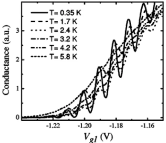
Finally, the temperature behavior of our device共see Fig. 4兲 shows that the effect is still present up to 4.2 K, consistent with the CB charging energy UCBpreviously found.
We wish to point out an advantage intrinsic to this scheme with respect to quantum devices based on coherence effects: as for the case of single electron transistors,20,21 ap-propriate geometries and materials can lead to higher and even room-temperature operation of such CB-based direc-tional coupler. Available transconductance values are very high. In fact at low temperatures switching voltages are in the millivolt range and at least one order of magnitude lower than those required in Y-branch devices共operated both in the FIG. 2. Schematic of our device. QD indicates the quantum-dot location
共black circle兲. Black regions represent the metal gates while gray areas show
the regions depleted by the applied bias.
FIG. 3. Conductance behavior of the QD at finite bias共left panel兲 and in magnetic field parallel to the 2DEG共right panel兲. T=350 mK.
052102-2 Pingueet al. Appl. Phys. Lett. 86, 052102共2005兲
so-called “external side-gate”7 and in “internal ballistic” switching mode8兲. This leads to measured normalized-transconductance values as high as I−1dI / dVg1⬃1500 V−1 for collector B in the present implementation. This charac-teristic is of interest in terms of low power consumption for high miniaturization and large scale integration.
In conclusion, a directional coupler device based on CB was demonstrated. Its differential-conductance characteriza-tion as a funccharacteriza-tion of magnetic field and temperature was presented. In the CB regime this device behaves like a cur-rent switch in one collector output and as a curcur-rent modula-tor in the opposite one. The same basic scheme can be em-ployed to design logic functions or, employing a series of our device, a CB-based electronic multiplexer.
Fruitful discussions with S. de Franceschi and M. Gov-ernale are gratefully acknowledged. This work was sup-ported in part by the European Research and Training
Net-work COLLECT共Project No. HPRN-CT-2002-00291兲. Work at NEST-INFM was supported in part by MIUR under FIRB Contract No. RBNE01FSWY, and work at Cavendish Labo-ratory by EPSRC.
1
J. A. del Alamo and C. C. Eugster, Appl. Phys. Lett. 56, 78共1990兲. 2
C. C. Eugster and J. A. del Alamo, Phys. Rev. Lett. 67, 3586共1991兲. 3
C. C. Eugster, J. A. del Alamo, M. J. Rooks, and M. R. Melloch, Appl. Phys. Lett. 64, 3157共1994兲.
4
N. Tsukada, A. D. Wieck, and K. Ploog, Appl. Phys. Lett. 56, 2527
共1990兲.
5
N. Tsukada, M. Gotoda, M. Nunoshita, and T. Nishino, Phys. Rev. B 53, R7603共1996兲.
6
T. Palm and L. Thylen, Appl. Phys. Lett. 60, 237共1992兲. 7
L. Worschech, B. Weidner, S. Reitzenstein, and A. Forchel, Appl. Phys. Lett. 78, 3325共2001兲.
8
K. Hieke and M. Ulfward, Phys. Rev. B 62, 16727共2000兲. 9
J. Wang, H. Guo, and R. Harris, Appl. Phys. Lett. 59, 3075共1991兲. 10
O. Vanbésien and D. Lippens, Appl. Phys. Lett. 65, 2439共1994兲. 11
Y. Takagaki and K. Ploog, Phys. Rev. B 49, 1782共1994兲. 12
Y. Hirayama, A. D. Wieck, T. Bever, K. von Klitzing, and K. Ploog, Phys. Rev. B 46, 4035共1992兲.
13
H. van Houten and C. W. J. Beenakker, Phys. Rev. Lett. 63, 1893共1989兲. 14
A. A. M. Staring, H. van Houten, C. W. Beenakker, and C. T. Foxon, Phys. Rev. B 45, 9222共1992兲.
15
L. P. Kouwenhoven, C. M. Marcus, P. L. McEuen, S. Tarucha, R. M. Westwervelt, and N. S. Wingreen, in, Mesoscopic Electron Transport, ed-ited by L. L. Sohn, L. P. Kouwenhoven, and G. Schön共Kluwer, Dordrecht, 1997兲, Vol. 345, p. 105.
16
J. Weis, R. J. Haug, K. V. Klitzing, and K. Ploog, Phys. Rev. Lett. 71, 4019共1993兲.
17
D. S. Duncan, D. Goldhaber-Gordon, R. M. Westervelt, K. D. Mara-nowski, and A. C. Gossard, Appl. Phys. Lett. 77, 2183共2000兲. 18
J. A. Folk, C. M. Marcus, R. Berkovits, I. L. Kurland, I. L. Aleiner, and B. L. Altshuler, Phys. Scr. 90, 26共2001兲.
19
S. Lindemann, T. Ihn, T. Heinzel, W. Zwerger, K. Ensslin, K. Maranowski, and A. C. Gossard, Phys. Rev. B 66, 195314共2002兲.
20
T. A. Fulton and G. J. Dolan, Phys. Rev. Lett. 59, 109共1987兲. 21
J. Shirakashi, K. Matsumoto, N. Miura, and M. Konagai, Appl. Phys. Lett.
72, 1893共1998兲.
FIG. 4. Temperature behavior of the CB effect in the collector B: conduc-tance oscillations are present from 0.35 up to 4.2 K.
052102-3 Pingueet al. Appl. Phys. Lett. 86, 052102共2005兲