Trapping and detrapping effects in high-quality chemical-vapor-deposition diamond films:
Pulse shape analysis of diamond particle detectors
Marco Marinelli, E. Milani, A. Paoletti, A. Tucciarone, and G. Verona-Rinati
INFM-Dipartimento di Scienze e Tecnologie Fisiche ed Energetiche, Universita` di Roma ‘‘Tor Vergata,’’ Via di Tor Vergata, I-00133 Roma, Italy
M. Angelone and M. Pillon
Associazione EURATOM-ENEA sulla Fusione, Via E. Fermi 27, I-00044 Frascati (Roma), Italy 共Received 12 February 2001; published 19 October 2001兲
An analysis of the time evolution of the response of diamond particle detectors is carried out, using as a probe 5.5 MeV ␣ particles impinging on high-quality diamond films grown by microwave chemical vapor deposition共CVD兲. Both the amplitude and the time evolution of the pulses are shown to change drastically when the detector is preirradiated with particles 共pumping兲, a slow component developing after pumping, indicating carriers trapping and releasing共detrapping兲. Pulse shapes obtained for positive and negative detector polarities are compared in both the as-grown and pumped states. The presence of at least two trapping centers for holes is necessary to explain the results, the shallower having an activation energy of about 0.3 eV. The effects of pumping are clarified, and the different role played by electrons and holes is evidenced. We modify a previous model for trapping-detrapping behavior originally applied to Si共Li兲 detectors to describe the more complex behavior of CVD diamond detectors, and develop a computer simulation based on it. The simulated pulse shapes agree very well with experiment with reasonable values of the physical parameters involved, making this technique helpful for studying and identifying defects which are responsible for limitation of the efficiency of CVD diamond particle detectors. Field-assisted detrapping seems to take place for fields of about 104V/cm.
DOI: 10.1103/PhysRevB.64.195205 PACS number共s兲: 61.82.Fk, 61.72.⫺y, 81.05.Tp, 29.40.Wk
I. INTRODUCTION
With the next generation particle accelerators, the conven-tional silicon-based particle detectors will not be able to sus-tain the high projected particle fluxes without rapid deterio-ration. Possible alternatives are ‘‘hardening’’ treatments of silicon or the use of new materials, among which diamond shows extremely high radiation hardness.1 In addition, dia-mond presents interesting electronic properties,2such as high carrier mobility, a high energy gap resulting in a very low number of free carriers, and a very high breakdown field, thus in principle making low noise, fast diamond based detectors feasible.
Because of its cost, moderate size, and lack of standard-ization natural diamond is not suitable for such an applica-tion. High-pressure synthesized diamond detectors with ex-cellent properties have been realized3but mainly because of size problems most of the research in this field is focused on nuclear detectors based on synthetic diamond films grown by chemical vapor deposition 共CVD兲, whose performances are studied in many research institutes, commercial diamond producers, and particle accelerators plants 共see, e.g., the RD42 activity at CERN兲.1
Efficient particle detection requires high drift lengths of the carriers produced by the ionizing particle and is therefore highly sensitive to film quality. Therefore a severe limitation for this as well as for many other applications of diamond is the presence of defects and the polycrystalline nature of CVD diamond films. It is important both to realize high qual-ity diamond films and to understand the role of defects and grain boundaries in the detection mechanism. Due to the
complexity of CVD diamond, very little is known nowadays on this subject.
An interesting feature is the priming共or pumping兲 effect, which is widely used to increase CVD diamond detector per-formance. It consists of a preirradiation of the CVD diamond detector by ionizing radiation. The increased efficiency is believed to be due to a saturation of deep traps. In spite of the importance of this effect, only a few authors studied the relationship between pumping and the microscopic structure of CVD diamond.4 – 6
The performance of diamond particle detectors and the effects of pumping are generally described through the charge collection distance and the efficiency, which we de-fine below. In a standard experimental setup in which a par-allel plate detector of thickness 共i.e., electrode spacing兲 d is used, each electron-hole pair created by an ionizing particle induces7,8 in the external circuit a charge qc⫽ex/d,x being the total distance that the electron and hole move apart under the action of the applied electric field before either reaching the electrode or being trapped, and e being the electronic charge. The amplitude of the voltage pulse measured by the external circuit is proportional to the total collected charge Qc 共i.e., the sum of qcover all electron-hole pairs produced by the ionizing particle兲 and the time evolution of the pulse depends on carriers’ dynamics. The ratio
⫽Qc/Q0 共1兲
between Qc and the total charge Q0 generated by the ioniz-ing particle in the detector is the detector’s efficiency. Clearly,depends on the average drift distance
␦⫽共e⫹h兲E, 共2兲 where e,h are the electron and hole mobilities, respec-tively, is the mobility weighted lifetime of electrons and holes, and E is the applied electric field. The average drift distance␦is also referred to as the charge collection distance
共CCD兲.
The statistical distribution of the amplitudes of the pulses generated by the incoming radiation共i.e., the charge collec-tion spectrum; see Fig. 1 for a typical spectrum of our detec-tors in the pumped state兲 is the preferred tool to analyze the behavior of particle detectors, showing both the amplitude of the response to particle irradiation 共that is, the induced charge and therefore the detector’s efficiency and CCD兲 and the inhomogeneity of the response共that is the energy resolu-tion兲. However, apart from these performance parameters, limited information on the physical process leading to par-ticle detection can be obtained from the charge collection spectrum. Recently4a model discussing the role of in-grain defects and grain boundaries in determining the response of detector grade CVD diamond films has been proposed which relates the change in the shape of the charge collection spec-trum before and after pumping to the distribution of defects. Soon after,5this model was found to be able to quantitatively explain the dependence of efficiency and CCD on the thick-ness of CVD diamond detectors in the as-grown and pumped states, taking into account the polycrystalline nature of CVD diamond and its columnar growth.
An interesting technique which has been used by several authors to collect information on the efficiency and CCD of diamond samples is ion beam induced charge 共IBIC兲. In IBIC a beam of ions 共typically protons兲 is focused in a micrometer-size spot on the surface of a diamond detector, so that information on the local efficiency and CCD of the sample can be extracted. The detector area is then scanned to obtain a two-dimensional 共2D兲 map of the geometrical distribution of efficiency and CCD over the detector’s area. With this technique it has been shown that the response of CVD diamond detectors is inhomogeneous9,10 and that pumping increases the efficiency of ‘‘bad’’ regions.6 Al-though very powerful, thanks to its spatial resolution, the IBIC technique provides limited information concerning car-rier dynamics.
A deep insight on the dynamics of charges generated in the detector can be obtained from the time development of single pulses. Zanio et al.11 and Martini and McMath12 showed how this time behavior changes when detrapping and/or trapping events occur in the detector, and applied this analysis to conventional Si detectors. In this paper we present the time evolution of charge pulses in detector grade CVD diamond films and, by extending the approach of Mar-tini and McMath to describe the more complex behavior of CVD diamond detectors, succeeded in describing the trapping-detrapping processes taking place in CVD diamond, uncovering the different role played by electrons and holes. The effects of pumping are especially investigated. A com-puter simulation based on this model is shown to agree well with the experimental data, thus allowing the extraction of quantitative information. Since the dynamics of carriers gen-erated in the detector are determined by the presence of traps and defects, this technique is not just a method to character-ize diamond nuclear detectors, rather it is a powerful tool that can be usefully applied to any kind of CVD diamond film to extract information on the identity of defects existing in CVD diamond.
II. EXPERIMENT
Several detector grade CVD diamond films have been de-posited on silicon substrates13,14in a microwave tubular re-actor, suitably modified to improve film quality.15A conven-tional scratching procedure was adopted in order to promote diamond nucleation on Si surface. The gas mixture used is 1% CH4in H2, resulting in a growth rate of about 0.7m/h at the deposition temperature of 750 °C. Film thickness var-ied from about 20 m to about 100 m, depending on the deposition time, and was measured with a digital thickness meter. The films showed excellent crystal quality, with very narrow diamond Raman peaks共FWHM about 2.4 cm⫺1兲 and extremely low photoluminescence background.15
Particle detectors were then realized by thermally evapo-rating a circular Au contact about 5 mm2in size and 100 nm thick as the top electrode, while Ag paste was used as the silicon backing contact. The detector response to 5.5 MeV␣ particles, having a penetration depth of about 15m in dia-mond, was studied using 241Am source. The irradiation was carried out through a pinhole, in the normal direction to the sample surface. To measure the charge collection spectra the detector output has been connected, through a charge pre-amplifier and a shaping pre-amplifier with a 2 s shaping time, to a multichannel analyzer.
The charge collection spectra of the detectors were mea-sured both in the as-grown state and after preirradiation with 90Srparticles for about 60 h共3 krad total dose兲, necessary to drive the film in a fully pumped state. A typical charge collection spectrum of our samples is reported in Fig. 1. This particular film is 100m thick, as coming from a deposition time of about 150 h, is in the pumped state, and the applied voltage is 100 V. The average efficiency is about 40%共to be compared to the as-grown value of 9%兲 corresponding to an average CCD of about 85 m. Maximum values are about 65% and 185m, respectively. These high values reflect the
FIG. 1. Typical␣-particle collection spectrum of our films in the pumped state. Inset: geometry of the parallel-plate detector.
high film quality. In all cases the whole film has been utilized to build the detector, i.e., without removing the low quality layer close to the substrate interface, a procedure normally used to increase the detector performance共see, e.g., Ref. 1兲. Since ␣ particles are irradiated on the growth surface and their penetration depth is about 15m, this does not signifi-cantly reduce efficiency in thick films.
All the pulse time shapes have been measured on our samples using a fast digital oscilloscope, and have been cor-rected for the 3.2 s decay time of the electronics as dis-cussed below.
III. TRAPPING-DETRAPPING MODEL
Measuring the shape of the transient response of CdTe particle detectors Zanio et al.11found that it is influenced by the presence of carriers trapping and release共detrapping兲 by defects. On this basis Martini and McMath12 quantitatively analyzed the behavior of Ge共Li兲 and Si共Li兲 detectors devel-oping a model involving a single carrier type generated at one electrode and a single trapping center. In this case a single charge moving with drift velocity v from one
elec-trode to the other one in a parallel plate detector of thickness d contributes by dq⫽(ev/d)dt to the total charge induced in the external circuit as a result of Ramo’s theorem. Introduc-ing the transit time TR⫽d/v, i.e., the time necessary for a carrier to traverse the detector in the absence of trapping processes, for t⬍TRno charge reaches the electrode and the rate equation for free carriers is
dn dt⫽⫺ n ⫹⫹ 共n0⫺n兲 D , 共3兲
where n0 is the number of carriers generated by the ionizing particle,⫹is the trapping共i.e., free drift兲 time constant, and D is the detrapping time constant. By using Ramo’s theo-rem, Eq. 共3兲 leads to
Q共t兲⫽Q0e TR
冋
t D⫹ e ⫹共1⫺e⫺t/e兲册
, 共4兲with Q0 the total charge generated by the ionizing particle at the electrode and e⫽⫹D/(⫹⫹D). This formula holds for t⬍TR, since afterwards some charges reach the electrode and the total number of carriers in the detector changes. As shown by Eq.共4兲, the time evolution of the pulses generated by an ionizing particle in a parallel plate detector depends on the defects present in the detector. In the absence of trapping defects the pulse rises linearly with time up to the transit time TR at which all charges generated are collected at the electrodes关Eq. 共4兲 with ⫹→⬁兴. In this case the detector’s efficiency is 100%. Traps reduce the efficiency 共i.e., the pulse amplitude兲 if they do not allow thermal detrapping; otherwise 100% efficiency is still achieved, but the time re-sponse is now slower. Carriers experiencing trapping-detrapping have their motion delayed by a time of the order of the detrapping time constant, so that the charge collection process extends beyond the transit time TR i.e., outside the region of validity of Eq. 共4兲. For a 100m thick diamond detector working under an external field E⫽104V/cm, TR
⫽d/v⬇d/E⬇1 ns, so that in most cases the transit time in diamond detectors is shorter or comparable to the response time of the instrument used to trace pulse shapes, and the ‘‘fast’’ component described by Eq. 共4兲 may not be experi-mentally accessible. Charge collection for t⬎TR 共the so-called ‘‘slow’’ component of the pulse兲 is ruled by the de-trapping time constant which can be much longer than a few nanoseconds, so that it can be experimentally measured.
Unfortunately the time behavior of this ‘‘slow’’ compo-nent is not accessible analytically even in this simple case involving a single type of trapping center and a single type of carrier generated at one electrode. Moreover, such a simple model cannot be applied to diamond detectors under ␣- or -particle irradiation. In this case the released charge Q0 is not concentrated at one electrode but distributed along the particle penetration depth, ranging from several microns to the whole sample thickness; consequently both electrons and holes can in principle contribute to charge collection. In ad-dition, we will show in the following that more than a single type of defect must be introduced to explain experimental results in the case of CVD diamond detectors. A computer simulation can be used anyway to quantitatively describe trapping-detrapping effects once a qualitative picture of the trapping centers present in the detectors is available. The following section describes this procedure.
IV. RESULTS AND DISCUSSION A. Qualitative analysis
We now examine the experimental time evolution of the pulses before pumping 共i.e., in the as-grown state兲. Let us consider the same film whose spectrum in the pumped state is reported in Fig. 1. The pulses are plotted in Fig. 2 for the sample in the as-grown state under negative field polarity
共the behavior for positive field polarity is very similar; see
below兲. The applied voltage is 100 V, corresponding to an electric field of 10 kV/cm. After the initial fast rise, a slow decrease is found for all pulses. In all cases, this decrease is very well fitted by an exponential with a 3.2s time constant and it is therefore due to the electronics. In the following, all
FIG. 2. Time evolution of the pulses measured in the as-grown state on the same film whose spectrum is reported in Fig. 1. The applied electric field is 10 kV/cm, with negative polarity. The con-tinuous line is a fit of one of the pulses by an exponential with a 3.2
pulses are corrected for this decay, so that their time behavior represents the actual detector response. Replotting the pulses measured in the as-grown state 共for both positive and nega-tive field polarity兲 after correction we obtain Fig. 3. It is evident that the pulses have different amplitudes, reflecting the width of the charge collection spectrum. However, simi-lar amplitudes are observed for positive and negative posimi-lar- polar-ity. The most important feature is that in all cases the satu-ration value is immediately reached, the collected charge being constant after the 10 ns rise time of the digital oscil-loscope. This implies that once trapped by a defect, electrons and holes are not detrapped. Since thermally activated de-trapping effects do not significantly contribute to charge col-lection, the defects limiting the detector’s response in the as-grown state are identified as deep ones. The density of these trapping centers is such that the CCD is about 12m5. No significant difference is observed between positive and negative polarity because CCD共and even more so both elec-tron and hole mean free paths before trapping兲 is lower than the penetration depth G⬵15m of 5.5 MeV ␣ particles in diamond, so that the growth surface boundary plays a very limited role. Further, since the film thickness is dⰇ␦ the substrate interface boundary plays no role at all. Therefore, even if electrons and holes should have different mean free paths, no difference would be observed between negative and positive polarity. In principle only one kind of trap for electrons and holes is necessary to explain the behavior in the as-grown state.
This picture changes when examining the pulse shapes for the same sample, but in the pumped state, which are plotted in Fig. 4. No significant change occurs in the case of nega-tive polarity with respect to the unpumped state. A dramatic change, on the other hand, can be seen for positive field polarity. Not only is the amplitude of the pulses greatly en-hanced, reflecting the large increase of efficiency due to pumping, but a significant slow component develops. The symmetry between positive and negative polarity is therefore now broken.
To explain this behavior it is necessary to assume that another kind of defect becomes important in the charge col-lection process after pumping, namely a relatively shallow trap for holes, allowing detrapping. It seems that pumping
leads to a much higher mean free path for holes than in the as grown state, while the electron mean free path is not strongly affected. Thus, in the case of positive polarity holes are now substantially free to move along the 100 m film thickness towards the substrate interface, while for negative polarity they are collected at the upper electrode after having traveled at most a distance G⬵15m.
The simplest picture compatible with all experimental facts, including the development of the slow component, is therefore as follows. In the pumped state the mean free path of holes is greatly enhanced, because pumping saturates most of the deep defects responsible for hole trapping without de-trapping. Thus, shallower traps existing in a lower concen-tration than saturated, deeper ones, now become important. Since they allow detrapping, they do not limit the overall amplitude of the pulse, but slow down the process of charge collection. The main features of Fig. 4 are due to this effect. For positive polarity holes are now substantially free to travel through most of the sample via trapping-detrapping processes, thus leading to high collection efficiency4 and to the development of the slow component. For negative polar-ity, the limited changes in the pulse amplitude and shape with respect to the as-grown state show that no significant saturation of electron traps occurs. Holes are in principle substantially free to move, but since 5.5 MeV ␣ particles ionize only within their penetration depth G⯝15m from the detectors’ surface 共much less than the hole mean free path, see Table I兲, holes can move only a few microns before being collected at the upper electrode. They therefore cannot give a great contribution to charge collection according to Ramo’s theorem, nor can be trapped and detrapped since their mean free path is now much higher than the real path to the electrode. Therefore the slow component substantially does not show up, and at the same time the fast one does not increase significantly with respect to the as-grown case.
In conclusion, qualitative analysis of pulse shapes show that both deep共type A兲 and shallow 共type B兲 defects exist for holes, while only deep 共type A兲 defects are present for elec-trons. Note that, of course, A/B here simply stand for deep/ shallow, and by no means are A defects for holes physically identified with A defects for electrons.
FIG. 3. Pulses measured in the as-grown state for both positive and negative field polarity after correction for the electronics decay time.
FIG. 4. Pulses measured in the pumped state for both positive and negative field polarity after correction for the electronics decay time.
B. Computer simulation
Since the trapping-detrapping model seems to qualita-tively explain our results, we developed a computer simula-tion according to it, allowing us to calculate, in a discrete time approximation, the pulse shape Q(t). For each carrier type, the detector of thickness d is divided into N laminae, the transit time of a carrier in each lamina being⌬t⫽d/Nv
⫽TR/N, wherev is the drift velocity. For each type of car-rier 共electrons and holes兲 two kinds of defects 共A,B兲 are taken into account 共see above兲, having trapping time con-stantsA⫹,B⫹and detrapping time constantsAD,BD, respec-tively. Carriers can be free, ni(tj) being the number of free carrier in the ith lamina at time tj, or trapped in each of the two trapping centers, nAi(ti), nBi(ti) being their correspond-ing numbers. In the time interval⌬t⫽tj⫺tj⫺1, free carriers either move to the next layer contributing by ev⌬t/d⫽e/N
to the induced charge, or are trapped in either defect. In the same time interval, trapped carriers can be released and move to the next layer or remain trapped. We have therefore at first order approximation in⌬t:
ni共tj兲⫽ni⫺1共tj⫺1兲⫺ni⫺1共tj⫺1兲⌬t
冉
1 A⫹ ⫹ 1 B⫹冊
⫹nA共i⫺1兲共tj⫺1兲 ⌬t A D⫹nB共i⫺1兲共tj⫺1兲 ⌬t B D, 共5兲 nAi共tj兲⫽nAi共tj⫺1兲⫺nAi共tj⫺1兲 ⌬t A D⫹ni共tj⫺1兲 ⌬t A⫹ , 共6兲 nBi共tj兲⫽nBi共tj⫺1兲⫺nBi共tj⫺1兲 ⌬t B D⫹ni共tj⫺1兲 ⌬t B⫹ 共7兲 共release and trapping of a carrier in a single time interval ⌬tand other second order effects can be neglected for suffi-ciently large N values兲. The total charge induced by each type of carrier is then
Q共tj兲⫽Q共tj⫺1兲⫹ e N
兺
ini共ti兲. 共8兲
This procedure is repeated twice共for electrons and holes, respectively兲, and the results are summed. In Eqs. 共5兲–共7兲 direct recombination effects have been neglected since elec-trons and holes rapidly separate under the external electric field, and the concentration of charges generated along the ␣-particle track is estimated to be lower than that of trapping centers. Equations共5兲–共7兲 are the discreet counterparts of the differential equations n共x,t兲 t ⫽⫺v n共x,t兲 x ⫺ nA共x,t兲 t ⫺ nB共x,t兲 t , 共9兲 nA共x,t兲 t ⫽ n共x,t兲 A⫹ ⫺nA共x,t兲 A D , 共10兲 nB共x,t兲 t ⫽ n共x,t兲 B⫹ ⫺nB共x,t兲 B D , 共11兲
describing the charge densities n(x,t), nA(x,t), and nB(x,t). The model can be easily extended to include other types of defects.
In the general case, the parameters to be included in the simulation are the carrier velocity共which gives the value of
⌬t兲, and the time constants eA⫹ , eB⫹ , eA D
, eBD and hA⫹ , hB⫹ , hA
D , hB
D for electrons and holes, respectively. How-ever, in our case, according to the discussion reported in the previous section, the density of type B defects for electrons is taken to be zero共i.e.,eB⫹⫽⬁兲. Also, type A defects are deep ones and do not allow detrapping共eAD , hAD⫽⬁兲. OnlyeA⫹ , hA⫹ and eB⫹ , hB
D
must therefore be determined. Since the CCD is more easily visualized in terms of carrier mean free path, and trapping times are directly connected to mean free paths through the carrier velocity v, the parameters which
we will discuss are the mean free paths LeA⫽veA⫹ , LhA
⫽vhA⫹ , LhB⫽vhB⫹ due to type A or B defects for electrons and holes, respectively, and the detrapping time constant for holes, hBD . In the simulation, the carrier velocity has been fixed to 5 106cm/s.16 The total transit time of a carrier through the detector is therefore TR⫽d/v⫽2 ns, and all time constant values given are relative to this value, while the mean free path values do not depend onv and are therefore
real ones.
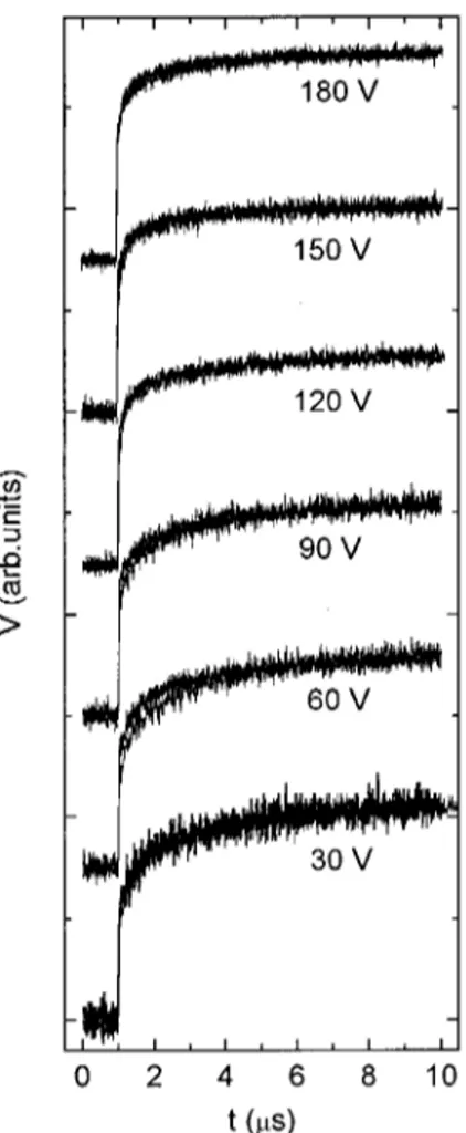
In Fig. 5 simulated pulses are compared with experimen-tal ones in the as-grown and pumped states for positive po-larity 共the negative polarity case is a trivial one, since the slow component is always very small兲. Because of the scal-ing property of the pulses described below, a sscal-ingle pulse for the as-grown and pumped states has been selected, chosen in the middle of the efficiency distribution determined by the ␣-particle collection spectra共i.e., about 8% in the as-grown state and about 40% in the pumped state兲.
The simulation describes very well the experimental be-havior of both curves using a single set of physical param-eters, whose values are reported in Table I. The procedure adopted to find the parameters values giving the best agree-ment with the measured pulses is as follows. First, the as-grown curve alone is simulated. Since, as discussed above,
FIG. 5. Comparison of measured pulses with the simulation based on the trapping-detrapping model.
the lack of a slow component for the as-grown detector in positive polarity means that the density of deep共A兲 traps for holes is much higher than that of shallow共B兲 traps, the only parameters to be determined are in this case LeA and LhA, the value of LhB being almost irrelevant. When, as in the present case, the efficiency is so low that the total CCD is lower than the penetration depth of ␣particles, the only ac-cessible information is the sum of electron and hole mean free paths and not their separate values. Therefore we set LeA⫽LhA and found that the as-grown state pulse is simu-lated using LeA⫽LhA⬵4.5m for a total CCD of about 9 m. This agrees well with the 12m value reported in Ref. 5 for samples thicker than 40 m, taking into account the fact that in the present work the applied field is 10 kV/cm, lower than the one used in Ref. 5 共15 kV/cm兲. With the chosen value for the carrier velocity, these mean free paths correspond toeA⫹⫽hA⫹⫽0.09 ns. Hence the pulse measured in the pumped state has been simulated introducing also shal-low共detrapping兲 hole traps 共i.e., LhB兲 and, as already argued in the preceding section, a substantially lower concentration of effective deep hole traps共i.e., a higher value for LhA兲 as a consequence of pumping. The concentrations of deep elec-tron traps 共i.e., LeA兲 is kept unaltered. In order to reproduce the experimentally observed amplitude ratio between fast and slow components it turns out that LhA⫽50m 共i.e., hA⫹⫽1 ns兲, so that the pumping process reduces the density of effective hole deep trapping centers by one order of mag-nitude, while LhB⫽35m 共i.e., hB⫹⫽0.7 ns兲, much higher than the 4.5 m as-grown value of LhA. This is consistent with our assumption that before pumping deep共type A兲 traps dominate hole dynamics 共coming from the lack of a significant slow component兲; thus the validity is confirmed of the initial assignment LeA⫽LhA⬵4.5m based upon ne-glecting hole type B traps in the simulation of the as-grown pulse.
The time evolution of the slow component is well de-scribed whenhBD⫽200 ns. From the 200 ns detrapping time a rough estimate of the activation energy EDof shallow de-fects responsible for hole trapping and detrapping can be made since 1/hB
D⫽s exp(⫺E
D/kT). Using s⬇1012s⫺1 for the attempt frequency共to which EDis anyway relatively in-sensitive兲 we obtain ED⬵0.3 eV. Finally, all parameters are introduced in the simulation and both curves are recalculated refining all parameters together, and the result is plotted in Fig. 5.
In agreement with the model, in much thinner films (d
⭐35m) a significant slow component is not detected even after pumping, since holes are trapped at the highly defective region close to the film-substrate interface before traveling distances much in excess of 10 m.
C. Field effect
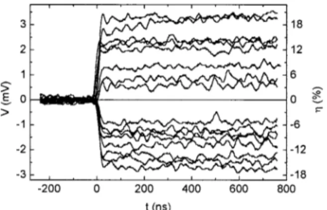
A very interesting feature of the pulses reported in Figs. 3 and 4 is the similarity of their shapes, in spite of the large differences in their amplitude. We therefore normalized them, and found that within the experimental noise, the nor-malized pulses superimpose well, except for small deviations in the region of the initial rise of the slow component. This scaling is rather obvious when only the fast component is present, but certainly not trivial in the case of the pulses measured for positive polarity on the detector in the pumped state, for which a consistent fraction of the collected charge comes from the slow component. This means that for all the reported pulses共which span an efficiency ‘‘window’’ roughly extending from 15% to 50%兲 the ratio between the fast and the slow component is very similar. This scaling would point in favor of a single, simple mechanism affecting the pulse amplitudes. It would have been tempting to attribute the dif-ferent pulse amplitudes, and therefore the broadening of the charge collection spectra, to electric field inhomogeneities due to the polycrystalline nature of CVD diamond.
To better clarify the role of the electric field we report in Fig. 6 normalized pulses measured at various applied volt-ages from 30 V to 180 V共corresponding to 3 kV/cm and 18 kV/cm, respectively兲. Pulses are grouped according to the applied voltage共3 pulses for each voltage, from low to high efficiency兲 and different groups are vertically shifted to in-crease readability. It can be seen that within each group pulses scale well, with the exception of a single pulse at 60 V, but as the voltage is increased the time behavior of the slow component speeds up. Two possible explanations are
共a兲 field enhanced detrapping, and 共b兲 the occurrence of
mul-tiple trapping-detrapping events which slow down the re-sponse at lower fields, when the transit time TR is increased. In the latter case, the simulation shows that to account for the observed speed up, the transit time TR should change by a factor comparable to the sixfold increase in field, so that the ratio between trapping times and TRsweeps from above 1 to significantly below 1 共assuming that trapping times are not affected in the same way by carrier drift velocity, i.e., the cross section decreases with the carrier drift velocityv兲. This
seems unlikely since at fields of the order of about 104V/cm
共i.e., of the order of the ones used by us兲 the carrier drift
velocity of natural diamond is close to saturation. Moreover, the substantial constancy of the ratio between the slow and fast components which appears from Fig. 6 seems to rule out this possibility as the main source of pulse speedup.
Indeed, in the approximate case when the ionized charge is generated at one electrode, and the detrapping time con-stant is much longer than the trapping time concon-stant as it is in our case, the ratio between the slow and fast components can easily be analytically calculated. In this case, the fast com-ponent is clearly given by Eq. 共4兲 with t⫽TR and D⫽⬁, i.e., by h(储⫹/TR), where 储⫹⫽A⫹B⫹/(A⫹⫹B⫹) and h(x) TABLE I. Fitting parameters used in the simulation of Fig. 5.
LeA, LhAare the mean free paths due to type A defects for electrons and holes, respectively, LhBis the mean free path for holes due to type B defects, andhBD is the detrapping time constant for holes.
Before pumping After pumping
LeA共m兲 4.5 4.5
LhA共m兲 4.5 50
LhB共m兲 35 35
hBD
⫽x„1⫺exp(⫺1/x)… is the Hecht function of argument x. On
the other hand, the total efficiency is given by the same for-mula in which detrapping centers, which do not lead to loss of signal, are removed 共i.e., 储⫹⫽A⫹兲 and therefore by h(A⫹/TR). The ratio R between the slow and the fast com-ponent is then given for a single carrier by
R⫽h共A
⫹/T
R兲 h共储⫹/TR兲
⫺1, 共12兲
so that R only depends on the ratio between trapping times and TR.
According to Eq. 共9兲, and using the parameter values found in Sec. IV B, when TR is varied by a factor of 6 from 0.7 ns to 4 ns, R should change from 1.21 to 0.34, while the total efficiency increases from 17% to 47%. Although the model does not take into account all the features of polycrys-talline diamond, according to Fig. 6 it would seem that mul-tiple trapping-detrapping effects should not be the main source of the pulse speedup. Also, higher fields do not lead to a marked change in the slow to fast component ratio since, in the range of fields explored by us, the carrier drift velocity is close to saturation so that TR is not strongly affected by the field. Field-assisted detrapping is therefore likely to occur at the highest fields. Although EDis relatively high in our case, field-assisted detrapping has been observed in CdS共Ref. 17兲 and Se 共Ref. 18兲 (ED⬵0.1 eV), and the speedup effect shown in Fig. 6 is not dramatic given the sixfold increase in field.
Qualitatively similar results have been obtained on other samples, so that the described behavior can be considered as a general property of our high quality CVD diamond films.
V. CONCLUSIONS
An analysis of the time pulse shape of particle detectors built from high quality CVD diamond films has been carried out. It is found that the pulse amplitude and shape depend on the field polarity and is dramatically affected by pumping. These changes are interpreted in the framework of the trapping-detrapping model originally applied to Si-based detectors.12 To explain the particular features found in this work the original model has to be modified to reflect the higher complexity of CVD diamond. A computer simulation based on the model gives a pulse shape which agrees well with the observed ones. Valuable information concerning the nature of trapping centers for electrons and holes is provided by the analysis of pulse shapes. In particular, at least two different trapping centers for holes are identified, the shal-lower of the two having activation energy close to 0.3 eV.
The effect of pumping, which results in an increased am-plitude and in the development of a slow component for positive field polarity, is explained, allowing us to enlighten the role of pumping in the detector’s performance and the different behavior of electrons and holes. A remarkable fea-ture is the apparent scaling共within the experimental noise兲 of pulses measured in a given condition, which all have the same shape, independently from their amplitude. The behav-ior of the response under increasing electric fields leads to the conclusion that field enhanced detrapping occurs at fields close to 104V/cm.
1W. Adam et al., in 5th International Symposium on Diamond Ma-terials, Paris, France, 1997, edited by J. L. Davidson et al., Proceedings of the Electrochemical Society Vol. 97-32 共Electro-chemical Society, Pennington, NJ, 1998兲, p. 491.
2D. R. Kania, in The Physics of Diamond, edited by A. Paoletti and A. Tucciarone共IOS Press, Amsterdam, 1997兲.
3Y. Tanimura, J. Kaneko, M. Katagiri, Y. Ikeda, T. Nishitani, H. Takeuchi, and T. Iida, Nucl. Instrum. Methods Phys. Res. A 443, 325共2000兲.
4M. Marinelli, E. Milani, A. Paoletti, A. Tucciarone, G. Verona Rinati, M. Angelone, and M. Pillon, Appl. Phys. Lett. 75, 3216 共1999兲.
FIG. 6. Normalized pulses grouped according to the voltage applied during the measurement 共from 30 V to 180 V in 30 V increments兲.
5M. Marinelli, E. Milani, A. Paoletti, A. Tucciarone, G. Verona Rinati, M. Angelone, and M. Pillon, J. Appl. Phys. 89, 1430 共2001兲.
6
C. Manfredotti, F. Fizzotti, A. LoGiudice, P. Polesello, E. Vittone, R. Lu, and M. Jaksic, Diamond Relat. Mater. 8, 1597共1999兲. 7W. Shockley, J. Appl. Phys. 9, 635共1938兲.
8S. Ramo, Proc. IRE 27, 584共1939兲.
9C. Manfredotti, F. Fizzotti, A. LoGiudice, P. Polesello, E. Vittone, M. Truccato, and P. Rossi, Diamond Relat. Mater. 8, 1592 共1999兲.
10D. R. Beckman, A. Saint, P. Gonon, D. N. Jamieson, S. Prawer, R. Kalish, Nucl. Instrum. Methods Phys. Res. B 130, 518共1997兲. 11K. Zanio, W. Akutagawa, and J. W. Mayer, Appl. Phys. Lett. 11, 5
共1967兲.
12M. Martini and T. A. McMath, Nucl. Instrum. Methods 79, 259
共1970兲.
13G. Balestrino, M. Marinelli, E. Milani, A. Paoletti, I. Pinter, and A. Tebano, Appl. Phys. Lett. 62, 879共1993兲.
14M. Marinelli, E. Milani, M. Montuori, A. Paoletti, P. Paroli, and J. Thomas, Appl. Phys. Lett. 65, 2839共1994兲.
15M. Marinelli, E. Milani, A. Paoletti, A. Tucciarone, G. Verona Rinati, G. Messina, M. Angelone, and M. Pillon, Proceedings of the Applied Diamond Conference/Frontier Carbon Technology Joint Conference, Tsukuba, Japan共AIST, Tsukuba, Japan, 1999兲, p. 154.
16
S. Zhao, Ph.D. dissertation, Ohio State University, 1994. 17K. V. Boer and V. K. Kummel, Ann. Phys. 共Leipzig兲 14, 341
共1954兲.