N-type Organic Thin Film
Transistors (OTFT): Effects of
treatments of the
insulator/semiconductor interface
on the devices performances
Unione Europea UNIVERSITÀ DEGLI STUDI DI SALERNO
FONDO SOCIALE EUROPEO
Programma Operativo Nazionale 2000/2006 “Ricerca Scientifica, Sviluppo Tecnologico, Alta Formazione”
Regioni dell’Obiettivo 1 – Misura III.4 “Formazione superiore ed universitaria”
Department of Industrial Engineering
Ph.D. Course in Industrial Engineering
(XV Cycle-New Series, XXIX Cycle)
N-type Organic Thin Film Transistors (OTFT):
Effects of treatments of the
insulator/semiconductor interface on the devices
performances
Supervisors
Ph.D. Student
Prof. Alfredo Rubino
Maria Rosa Fiorillo
Tutor ENEA Ing. Paolo Tassini
Scientific Referees
Prof. Francesco Della Corte
Dr. Luigi Mariucci
Ph.D. Course Coordinator
List of works
Journal papers
Electrical model for admittance spectroscopy in n-type thin film transistors
M. R. Fiorillo, R. Liguori, C. Diletto, P.Tassini, M. G. Maglione, P. Maddalena, C. Minarini,A. Rubino, in preparation
Influence of the fabrication processes on the gate bias-stress effects in TIPS-pentacene OTFTs
R. Rega, P. Tassini, A. De Girolamo Del Mauro, G. Pandolfi, E. Calò, T. Fasolino, M. R. Fiorillo, A. Negrier, R. Miscioscia, M. G. Maglione, C. Minarini, P. Maddalena, H. L. Gomes, in preparation
Conference proceedings
Trap Density Analysis in PC70BM n-type Thin Film Transistors through
Admittance Studies
M. R. Fiorillo, R. Liguori, C. Diletto, E. Bezzeccheri, P.Tassini, M. G. Maglione, P. Maddalena, C. Minarini, A. Rubino, Materials Today: Proceedings 4, Salonicco, submitted
PC70BM n-type thin film transistors: Influence of HMDS deposition
temperature on the devices properties
M. R. Fiorillo, C. Diletto, P. Tassini, M. G. Maglione, E. Santoro, F. Villani, R. Liguori, P. Maddalena, A. Rubino, C. Minarini, Materials Today: Proceedings 3, 720-726, Salonicco, December 2016
Evaluation of the stability of different encapsulated blue oleds
E. Santoro, S. Aprano, G. Sico, M. R. Fiorillo, M.G. Maglione, P. Tassini, A. Rubino, C. Minarini, IET Conference Publications, Torino, Maggio 2015
Poster
SINFO 2016 - Methods for studying and improving performance of organic
electronic devices
S. Aprano, E. Bezzeccheri, M. R. Fiorillo, R. Liguori, E. Santoro, A. Rubino, C. Diletto, M. G. Maglione, G. Sico, P. Tassini, C. Minarini, Napoli, Giugno 2016
EOS’15 - Fabrication and characterization of a blue OLED based on
α-NPD as emitting-layer
S. Aprano, E. Santoro, M. Tesoro, C. T. Prontera, C. Diletto, M. R. Fiorillo, G. Cuomo, V. Criscuolo, P. Manini, A. Pezzella, G. Sico, M. G. Maglione, P. Tassini, A. Rubino, C. Minarini, Capri, Settembre 2015
GE Conference 2015 - Study and fabrication of selected organic electronic
devices to improve performance and stability
S. Aprano, E. , Bezzeccheri,M. R. Fiorillo, R. Liguori, E. Santoro, A. Rubino, C. Diletto, M. G. Maglione, G. Sico, P. Tassini, C. Minarini, Siena, Giugno 2015
Nanotech Italy 2013 - Development of phosphorescent OLEDs for general
lighting applications
M. G. Maglione, S. Aprano,P. Tassini, M.R. Fiorillo, E. Santoro, V. Criscuolo, P. Manini, A. De Girolamo Del Mauro, R. Rega, G. Pandolfi and C. Minarini, Venezia, Novembre 2013
Contents
Contents ... I
List of Figures ... III
List of Tables ... IX
Abstract ... XI
Introduction ... XIV
Chapter I Organic Semiconductors ... 1
I.1. Physics of Organic Semiconductors ... 2
I.2. Charge transport mechanisms ... 3
I.3. Charge carrier injection... 9
I.4. Defects in organic semiconductors ... 11
I.5. Organic electronics today and tomorrow ... 13
Chapter II Organic Thin Film Transistors ... 17
II.1. Thin-film Transistor fundamentals ... 17
II.2. Architectures ... 23
II.3. Materials ... 25
II.4. Operation Principle of OTFTs ... 28
II.4.1. Transistor Parameters ... 30
II.4.2. Non- ideal transistor behavior ... 31
II.5. Traps in OTFTs ... 34
II.6. Evolution of the OTFTs ... 34
Chapter III Fabrication of OTFTs ... 37
III.1. Architecture of the devices ... 38
III.2. Fabrication of the OTFTs ... 39
III.3. Cleaning of the SiO2 surface with UV/O3 treatment ... 40
III.4. Surface Treatments of Self-Assembled Monolayer (SAM) ... 42
III.4.1. Temperature dependence of the SAM formation ... 45
III.4.2. Time dependence of the SAM formation ... 46
III.5. Source and Drain Electrodes in OTFTs ... 47
III.6. Growth of Organic Semiconductor ... 49
Chapter IV Materials preparation and characterization and OTFTs DC analysis ... 53
IV.1. Analysis of HMDS Treatments ... 53
IV.1.1. Results of the experimental step ... 54
IV.3.1. Results of the experimental step... 61
IV.4. Discussion of the data - Comparing the electrical parameters vs. the hydrophobic characteristics ... 64
Chapter V Equivalent Circuit AC Model ... 67
V.1. AC Measurement ... 68
V.1.1. Results of the experimental step ... 69
V.2. Interface Characterization Technique ... 74
V.3. Equivalent electrical model ... 76
V.4. Models of the Bulk Traps Admittance ... 78
V.4.1. Single trap level - Data Fitting ... 79
V.4.1.1. Experimental data fitting and extracted parameters ... 81
V.4.2. Distribution of single trap levels- Data Fitting ... 86
V.4.2.1. Experimental data fitting and extracted parameters ... 90
V.4.3. Comparison between the models of single-level traps and of distribution of single trap-levels ... 95
V.4.4. Comparison of DC vs.AC parameters ... 96
Conclusion ... 99
Bibliography ... 103
List of Figures
Figure 1: Schematic representation of the formation of s and molecular orbitals from two carbon atoms with sp2 hybridization. ... 2
Figure 2: Representation of the transport mechanism in solids with applied
electric field, (a) for band transport conduction and (b) for hopping between localized states. ... 5
Figure 3: Distribution of trap states in the band gap for a p-type organic
semiconductor. ... 7
Figure 4: Hopping transport through the localized states in the Gaussian
disorder model (GDM). ... 8
Figure 5: Schematic energy level diagram of the band alignment at a metal
organic interface, (a) Mott-Schottky limit vacuum level alignment, and (b) pinning of the Fermi level by induced interface states interfacial dipole. ... 10
Figure 6: Representation of the energy levels of a host material with
chemical impurities (Pope & Swenberg, 1999). ... 12
Figure 7: Transfer characteristic of a pentacene transistor measured as
grown (blue line) and after oxidation (red line). The graph shows the
forward and the reverse sweeps in both cases. ... 13
Figure 8: Organic and printed electronics applications 6th edition of the
OE-A roadmap(2015). ... 14
Figure 9: Layer structure of an organic thin film transistor. ... 18
Figure10: (a)Electrical symbol of a TFT, and (b and c) two small-signal
equivalent circuits of a transistor, that show the gate-source capacitance CGS, the gate-drain capacitance CGD, the equivalent gate capacitance CG,
and the current source gm·vGS(Klauk, 2010). ... 18 Figure 11: Energy-level diagrams across the metal/dielectric/p-type
semiconductor interface of an organic transistor, showing (a)accumulation mode, (b) flat-band mode, (c) depletion mode. ... 20
Figure 12: Schematic operation regimes of p-type OTFT, (a) linear regime, (b) the start of saturation mode when the pinch-off point occurs, (c) the saturation regime. ... 22
Figure 14:General OTFT configurations: (a) staggered and bottom-gate top
contact; (b) coplanar and bottom-gate bottom -contact; (c) staggered and top-gate bottom-contact and (d) coplanar and top-gate top-contact. ... 24
Figure 15: Representation of a polymer: poly(3-hexylthiophene) (P3HT) (a),
and of conjugated small-molecule organic semiconductors: pentacene (b), sexithiophene (6T) (c), fullerene (C60) (d). ... 26 Figure 16:Trend vs. time of mobility for some p-type ( Pentacene and
Polythiophene) and n-type organic semiconductors (Kumar et al., 2014). .. 27
Figure 17:Typical electrical characteristics of an organic p-channel TFT:
output characteristics (a), input characteristics (Ig versus Vg) and transfer
characteristics (Id versus Vg) (b), transconductance gm versus Vg (c), and
carrier field-effect mobility in the linear and saturation regime (d), (Klauk, 2010). ... 30
Figure 18:Typical bias stress curves of two OTFTs. ... 33
Figure 19:Example of OTFTs applications: (a) banknote with OTFTs
embedded as an anti-counterfeiting feature, (b) Samsung prototype of flexible display, (c) organic logic circuits made by ink-jet printing, (d) biosensor for flexible backplanes. ... 35
Figure 20: (right) Substrate layout and (left) magnification of the
interdigitated fingers, with the specifications of the channel devices. ... 38
Figure 21:Schematic representation of the bottom-gate, bottom-contact
(BGBC) transistor architecture used.... 40
Figure 22:Description of a UV/O3 surface treatment system. ... 41 Figure 23: Formation mechanism of a generic SAM. ... 42
Figure 24: Chemical structure of HMDS hexamethyldisilazane
([(CH3)3Si]2NH)). ... 43 Figure 25: Formation of the hydroxyl groups during the UV/O3 treatment on
a substrate, (b) alkane chains during HMDS process, and the respective contact angles. ... 44
Figure 26: AFM images of partial SAMs growth at temperature of 10 °C, 25
°C, and 40 °C. ... 45
Figure 27: Depth distribution histograms for the sample at temperature of
10 °C, 25 °C, and 40 °C. ... 46
Figure 28: Average peak separation distribution, ∆h, as a function of the
time for samples processed at different temperatures. ... 47
Figure 29: SEM images of a pentacene thin film grown on SiO2 and on Au
electrode: untreated with SAM (a), treated with SAM of1-hexadecane thiol (b). ... 49
Figure 30: Chemical structures of the fullerene C60 (a) and fullerene
derivate PC70BM (b). ... 50 Figure 31: Description of the drop casting technique process applied in this
deposition. The interfacial tensions and the resulting SCA are indicated in red color. ... 54
Figure 33:Contact angle system Dataphysics OCA20 present at the ENEA
Research Centre in Portici. ... 55
Figure 34:Contact angle images for SiO2 substrates treated at different
HMDS deposition temperatures. ... 56
Figure 35:Shematic diagram of the working principle of AFM. ... 58
Figure 36: AFM images of PC70BM thin films deposited on SiO2 dielectric
treated with HMDS: (a) at 7°C; (b) at 25°C; (c) at 60°C. ... 59
Figure 37:Transfer curves of PC70BM based OTFTs obtained for HMDS
deposition at temperature of 7°C. ... 61
Figure 38:Transfer curves of PC70BM based OTFTs obtained for HMDS
deposition at temperature of 25°C. ... 62
Figure 39:Transfer curves (b) of PC70BM based OTFTs obtained for HMDS
deposition at temperature of 60°C. ... 62
Figure 40: Comparison of the output (a) and the transfer (b) curves for the OTFTs prepared using the HMDS deposited at the three different
temperatures; the two types of curves were respectively measured at VGS =
40V and VDS = 40 V. ... 63 Figure 41: Field effect mobility and threshold voltage of the fabricated
OTFTs vs. the contact angle of the substrate surface. ... 64
Figure 42: Schematic diagram of the characterization set-up for the AC
measurements of BC OTFTs. ... 68
Figure 43: Representative capacitance and loss curves for samples at 7°C
measured at various biases as a function of the signal frequency, (a) in linear scale and (b) in logarithmic scale. ... 70
Figure 44: Representative capacitance and loss curves for samples at 25°C
measured at various biases as a function of the signal frequency, (a) in linear scale and (b) in logarithmic scale. ... 71
Figure 45: Representative capacitance and loss curves for samples at 60°C
measured at various biases as a function of the signal frequency, (a) in linear scale and (b) in logarithmic scale. ... 72
Figure 46: Capacitance measured as a function of the gate voltage at the
fixed frequency of 100 Hz for samples at 7°C, 25°C and 60°C. ... 73
Figure 47: Capacitance and loss measured as a function of the frequency at
the fixed gate voltage of 40 V for samples at 7°C, 25°C and 60°C. ... 74
Figure 48: Band-bending diagrams as a function of the applied gate bias,
considering a device with OSC of p-type: (a) accumulation regime (negativegate bias), (b) flat-band (no gate bias), (c) depletion regime
(positive gate bias). HOMO e LUMO are highest occupied molecular orbital and lowest unoccupied molecular orbital, respectively; Ei is the intrinsic
Figure 49: Equivalent circuit used to represent the fabricated OTFTs in
BGBC configuration under analysis. ... 76
Figure 50: Representation of the contributions of the layers that make up the sample. The equivalent circuit is organized in four blocks: capacitance of overlap between S-D and gate electrode, semiconductor contribution, insulator contribution and contact resistance. ... 77
Figure 51: Representation of the two equivalent circuits of Yt(ω)for the
model of a single trap level. On the left-side, it is represented the series combination C network, and on the right-side, the parallel combination R-C network. ... 79
Figure 52: Plots of equivalent trap capacitance Ceq(ω) and equivalent trap
conductance Geq(ω)/ω as a functions of ωτ derived by eq.(33) and (34)
according to the model of a single trap level. ... 81
Figure 53: Fitting of the experimental data measured at VGS =40V (symbols)
according to the model (lines) of single-level traps for the admittance of the traps for a sample with HMDS deposition temperature of 7°C. Linear scale for the admittance axis. ... 83
Figure 54: Fitting of the experimental data at VGS = 40V (symbols)
according to the model (lines) of single-level traps for admittance of traps for the sample with HMDS deposition temperature of 7 °C. Logarithmic scale for admittance axis. ... 84
Figure 55: Channel resistance Rch (solid line) and density of the trap states
Dt (dashed line) vs. the contact angle of the surfaces of the samples treated
at the different HMDS deposition temperatures. ... 86
Figure 56: Representation of the band bending vs distance from the interface into the organic semiconductor. ET is the bulk trap level (dashed
line), while EF is the Fermi Level (solid line).This diagram shows that bulk
traps are active in a region of width (dv/dx)-1 near the crossover point, that corresponds to the region where bulk trap levels are within kT/q of the Fermi level. ... 87
Figure 57: Plots in logarithmic scale of the equivalent trap capacitance Ceq(ω) vs. ωτ for the model of a single trap level (dashed curve)as derived
from eq. (33) and for the model of a distribution of single trap levels (solid curve)as derived from eq. (39). ... 89
Figure 58: Plots in logarithmic scale of the equivalent trap conductance Geq(ω)/ω vs. ωτ for the model of a single trap level (dashed curve) as
derived from eq. (34) and for the model of a distribution of single trap levels (solid curve) as derived from eq. (40). The maximum for the distributed trap levels is at ωτn=1.98. ... 89 Figure 59: Fit of the experimental data, measured at different VGS (symbols),
according to the model (lines) of the distribution of single trap levels for the admittance of the traps for the samples with HMDS deposition temperature at7°C. Linear scale for the admittance axis. ... 91
according to the model (lines) of the distribution of single trap levels for the admittance of the traps for the samples with HMDS deposition temperature at 7°C. Logarithmic scale for the admittance axis. ... 91
Figure 61: Sheet channel resistance (Rch_sh), density of the trap states (Dbt)
and the relaxation time of the bulk trap level (τbt), calculated from the data
measured at VGS = 40 V, vs. the contact angle of the surfaces of the samples
treated at the different HMDS deposition temperatures, according to the model of the distribution of single trap levels. ... 94
Figure 62: Trend of the density of the trap states (Dbt) as a function of the
applied gate voltage (VGS), for all the samples treated at the different HMDS
deposition temperatures (7°C, 25°C, 60°C). ... 95
Figure 63: Comparison of the density of the trap states for the model of single-level traps (line orange) and for the model of a distribution of single trap levels (line green, for VGS= 40V. ... 96 Figure 64: Density of the interface trap levels Dbt and charge carrier
mobility µ vs. the contact angle of the surfaces of the samples treated at the different HMDS deposition temperatures. ... 97
Figure 65: Density of the interface trap levels Dbt and threshold voltage VT
vs. the contact angle of the surfaces of the samples treated at the different HMDS deposition temperatures. ... 98
List of Tables
Table 1: Summary of the surface treatment conditions and SiO2 contact
angle values. ... 56
Table 2: Roughness and grain mean size measurements of the PC70BM films
at the various SiO2 surface treatment conditions. ... 60 Table 3: Electrical parameters of the OTFTs for the different HMDS
deposition temperatures (mean values and errors from 20 samples). ... 63
Table 4:Summary of all the components extracted from the experimental data at VGS = 40 V according to the equivalent circuit. Extracted considering
CC = 700 pF ... 84 Table 5: Summary of all the components extracted from the experimental data at VGS = 40 V according to the equivalent circuit. Extracted considering
Abstract
The organic electronic devices are finding a great consideration for applications where silicon limitations make this semiconductor unsuitable. Many properties of organic materials open new frontiers of the research; some example of applications are flexible displays, smart textiles, new lighting fixtures, intelligent packaging. Furthermore, an interesting attraction of organic devices is their being environmentally friendly. Organic materials provide also an inspiration for always new applications stimulated by the continuing efforts of characterization, fabrication, synthesis and design.
This thesis work wants to contribute to the comprehension of the properties of solution processed organic thin film transistors (OTFTs) that use a n-type semiconductor. These devices are the basic element of the driving circuits, where the n channel transistors still result poorly understood. In this PhD activity, it is studied the effect of surface treatments at SiO2 dielectric layer and organic semiconductor interface to improve the
OTFTs performance. These transistors, that are fabricated employing a specific combination of treatments before the deposition of a soluble semiconductor, are studied in order to analyze the relationship between the surface treatments and the devices electrical parameters; so to calculate one or more variables able to better adapt the conditions of the treatments to the performances of the device.
The devices are fabricated using as semiconductor the [6,6]-phenyl-C71-butyric acid methyl ester (PC70BM) deposited from drop casting technique
on a SiO2 layer where a combination of ultraviolet/ozone cleaning (UV/O3)
and self-assembled monolayer (SAM) coating is previously carried out. The hexamethyldisilazane (HMDS) is the SAM used, and it is deposited at three different temperatures, 7°C, 25°C and 60°C. UV/O3 cleaning allows to
remove organic contaminations on the dielectric surface, thanks to the formation of hydroxyl groups (-OH) generated by the UV/O3 ambient. While
the HMDS can reduce the traps induced by Si-OH groups on the gate insulators, making layer treated hydrophobic. In this work, it is observed that different deposition temperatures of the SAM produce surfaces with
The techniques of analysis employed to observe the effects of the treatments have been: contact angle measurements, AFM imaging of the organic semiconductor, I vs. V static characterization and admittance measurements.
Particular effort is given to evaluate the presence of electronic trap states in organic thin film transistors based on n-type semiconductor in bottom-gate bottom-contact configuration, thus it is proposed a new and accurate equivalent electrical, which is capable to model the properties of the semiconductor bulk and the conductive channel, through the calculation of the density of the trap states and the channel resistance.
From the performed analysis, the transistors treated at temperature of 25°C show a high roughness, a very inhomogeneous surface of the semiconductor layer and a higher degree of the SiO2 surface hydrophobicity
compared to the transistors processed at 7°C and 60°C. The HMDS behaving as a silane coupling reactant, provides a better tailored hydrophobic surface during the processes at 7°C and at 60°C, resulting in an improved surface energy, matching between the gate insulator and the organic semiconductor.
From DC measurements, it is observed that the samples at 60°C temperature for HMDS deposition show the best performances: the highest electron mobility of 13·10-3 cm2/Vs and the lowest threshold voltage of 12.0 V. While for the devices prepared at 7 °C and at 25 °C, the values of the mobility and the threshold voltage are 7.6·10-3 cm2/Vs - 13.6 V, and 2.8·10-3 cm2/Vs - 17.8 V, respectively.
The densities of the resulting trap states, calculated by admittance measurements and equivalent circuit, show the minimum quantity of the traps for the devices treated at 60°C compared to other devices, with a value of 1.48 1016 cm-3 eV-1.
In conclusion, in this thesis it has been studied the effect of the deposition processing of HDMS layers on the behavior of PC70BM gate
bottom-contacts OTFTs. In particular, the temperature of the HMDS process influences the quality of the semiconductor films and the devices performances. The hydrophobicity of the dielectric surface, induced by the HDMS process at 60°C, measured trough the value of the contact angle, which is of the order of 104.1° for this process, results in the formation of the highest quality of the PC70BM films, with homogeneous layers and a
reduced quantity of traps, giving the OTFTs with the best performances. This results have allowed to develop a new equivalent electrical circuit, which, for the first time, models the AC behavior of gate bottom-contacts OTFTs with n-type semiconductors.
Introduction
The Organic Electronic devices have attracted large interest in the scientific community, as evidenced by the many groups of corporate and university research centers who work on these subject, including Philips, Samsung, Sony, but also the birth of associations such as OE-A (Organic and Printed Electronics Association), which includes more than 200 companies and research centers in the world, and promotes the creation of a competitive production infrastructure for organic and printed electronics.
Organic electronics is based on the combination of a new class of materials and large-area, high-volume deposition and patterning techniques. The peculiar mechanical properties of organics, the easiness of device manufacturing and the cheapness of the end products open the way to a wide range of applications, from flexible displays, to smart-card, up to wire devices for intelligent fabrics (smart clothing).
This technology is still in its early stage; while increasing numbers of products are available and some are in full production, many applications are still in lab-scale development, prototype activities or early production (Kirchmeyer et al., 2013).
The future of organic electronic is based on devices that are able to do things that are not possible for silicon-based electronics, expanding the functionality and accessibility of electronics, as the ability to create flexible and transparent devices. Organic electronic devices will be more energy-efficient than today’s electronics, and will be manufactured using more resource-friendly and energy efficient processes than today’s methods, contributing to a more sustainable electronic world.
Actually, many efforts have been done in order to develop the organic driving circuits, such as switches and memories, required for implementing a fully flexible, plastic electronics. In particular, for this aim, the interest is focused on solution processed organic thin film transistors (OTFTs) that could be the backbone of the plastic electronics.
A significant technological challenge is associated with the fabrication of organic complementary circuits, where deposition and patterning of the p- and n-channel semiconductors with high resolution is the objective pursued. The vast majority of organic complementary circuits reported in the
semiconductors. But, a proof of concept of the practical implementation of this technology in large-scale ICs is limited due to design constrains imposed by the shadow masks utilized for the semiconductor patterning. In this context, alternative deposition techniques (i.e. ink-jet printing, gravure printing, etc.) could potentially provide a long-term solution. In an effort to address this issue, significant research has focused on the organic semiconductors with useful solubility. As a result, a number of soluble p-channel semiconductors with carrier mobility comparable to amorphous silicon (a-Si) have been demonstrated and utilized in unipolar ICs. On the other hand, progress in the area of soluble n-channel semiconductors has been much slower with relatively few successful demonstrations. This distinct lack of soluble n-channel semiconductors has, to a large extent, hindered the development of large-scale organic complementary ICs (Wobkenberg & Anthopoulos, 2008).
In this context, this thesis work regards the fabrication of n-type OTFTs using the fullerene derivative [6,6]-phenyl-C71-butyric acid methyl ester (PC70BM) as the semiconductor. This molecule is soluble in various organic
solvents, allowing an easy deposition from solution and so being potentially much advantageous in the area of the large-area organic electronics.
The aims of the present research are the realization of n-type transistors with solution processed semiconductor to obtain good performance, as well as the understanding and the modeling of the mechanism involved in these unconventional materials.
A critical issue to be investigated in order to obtain good-performance OTFTs is the quality of the interfaces between the various layers constituting the device, particularly the interface between the semiconductor and the gate insulator, where the conductive channel is generated. For this purpose, in this work different processes are considered to improve the performance of the OTFTs, that are: the wafer cleaning procedures using an UV/O3
treatment, the application of surfaces modification using a self-assembled monolayers (SAM), and different temperatures during the depositions of SAM layer.
Static electrical measurements and AC electrical techniques have been borrowed by the world of the inorganic semiconductors in order to evidence all the aspects regarding the features of the organic semiconductors and the devices based on them. DC measurements represent a basic tool for the analysis of the properties of organic semiconducting materials, while AC electrical techniques give the possibility of probing the local contributions to the observed overall properties showed by organics and devices, such as the limiting charge trapping phenomena due to extrinsic localized defects and the trapping produced by the intrinsic defects due to the structural features of
proposed to interpret the data of the admittance measurements. This new RC network includes all the effects of OTFTs in bottom-gate bottom-contacts configuration and well describes the properties of dielectric/organic semiconductor (SiO2/PC70BM) interface.
In this context, the thesis work proposal regards the study of the interface and the related devices properties through the analysis of the grade of wettability of the dielectric surface after SAM deposition at different temperatures, the morphological analysis of the semiconductor layer in different conditions, and the application of both the methods of static and dynamic analysis of the electrical measurements.
The thesis is organized in five chapters. In the Chapter 1, it is presented a brief historical framework of the organic semiconductors, an overview on the principal features of the organic semiconductors and on their future applications. The Chapter 2 is dedicated to the organic thin film transistors, focusing the attention on ideal and non-ideal functioning principles, the devices architecture, the description of the extracted device parameters, the difference between p-type and n-type transistors, and possible new implementations of these devices. In the Chapter 3, it is described the fabrication process used to realize the samples and their analysis respect on some important parameters, as temperature and time. In particular, it is presented the architecture employed, the steps for the fabrication of the devices relatively to the description of UV/O3 and SAM treatments, source
and drain electrodes and deposition of the organic semiconductor. All activities carried out during the PhD activity are deal with in the Chapters 4 and 5. .
The experimental work was carried out at the ENEA Research Centre in Portici and in the Microelectronics Laboratory of the University of Salerno. All the fabricated devices have been processed in the cleanroom (class 100) located in ENEA, while the electrical characteristics are analyzed both at the ENEA and at University. The Chapter 4 is devoted to describe in detail the results of the experimental analysis to evaluate the fabrication processes adopted. Measurements of the contact angle and the semiconductor films morphology are part of this chapter. Furthermore, the results of the static characterizations of the OTFTs are presented. Thus, a part of the chapter is focused on the hydrophobic characteristics of the devices, with particular attention on the relationship between the grade of wettability and the devices performance. In the Chapter 5, the AC measurements of the devices admittance and a new model of the OTFTs AC behavior are presented. This model takes into account the devices geometry and the distribution of the traps levels in disordered semiconductors. The purpose of the proposed model is to evaluate the effect of the different treatments by extracting some interesting parameters that allow to compare them. Then, two models of the admittance associated with the traps are reported, together with fitting data and extracted parameters associated, respectively, to deepen the
devices. Finally, the AC parameters are compared with the resulting parameters of the DC measurements, to understand the efficacy of the treatments to improve the overall performance of the studied transistors.
Chapter I
Organic Semiconductors
In 1977 a new class of materials was discovered, their name was ‘conducting polymers’ (Shirakawa et al., 1977). These materials, now known as organic semiconductors, obtained significant interest of scientific communities in their properties and applications. This research consisted on the observation of increased electrical conductivity of halogen-doped polyacetylene, and for this work, Heeger, MacDiarmid, and Shirakawawere awarded the 2000 Nobel Prize in Chemistry.
In 1986 started the first applications of organic semiconductors: Tang reported a two-layer organic photovoltaic cell (OPV) using copper phthalocyanine (CuPc) and a perylenetetracarboxylic derivative as organic semiconductors (Tang, 1986) and, in the same year, an organic field-effect transistor (OFET) using polythiophene was first reported by Tsumura, Koezuka, and Ando (Tsumura et al., 1986). In 1987, Tang and VanSlyke realized organic light-emitting diodes (OLEDs) using an Alq3/diamine junction (Tang & VanSlyke, 1987). Even if the devices did not exhibit great performances, they were recognized as milestones about the electronic application of organic semiconductors, which lasts until present and is foreseen a very bright future.
The peculiarities of organics are given by their molecular nature, by weak intermolecular interaction. While for inorganic crystals all consisting atoms are strongly bound by covalent bonds, for organics the molecules are ‘weakly’ linked to each other by van der Waals force (Brown & Poon, 2004). Thus, this weak intermolecular interaction is responsible for the mechanical flexibility of the organic films or crystals. Furthermore, weak molecule-molecule bonds can be easily broken or reformed so molecules can be dispersed in solvents or evaporated at moderate temperature, allowing for various new process concepts for the organic semiconductors.
In this first chapter, it is shown a review on the fundamental physics and mechanism of charge injection into organic semiconductors (OSCs), and
I.1.
Physics of Organic Semiconductors
Organic materials are characterized by building blocks made up by various forms of hydrocarbon (C-H) units, which can also include heteroatoms such as nitrogen, sulfur, oxygen, etc (Brown & Poon, 2004). For their typical energy gap ranges (between 1.5 eV and 3.5 eV) and their few mobile or free carriers at room temperature, organic materials can be considered as insulators. But the organic materials can be defined as organic semiconductors that exhibit semiconducting properties, and corresponding to a subset of a vast variety of organic materials.
Carbon is a chemical element in the fourth group of the periodic table, so it contains four valence electrons. The electronic orbitals of a carbon atom may hybridize differently, depending on the number of atoms with which the valence electrons are shared (Kymissis, 2009). The valence electrons can be shared with four neighboring atoms, to form four chemical bonds and four equivalent degenerated orbitals, referred to as sp3 hybrid orbitals in a tetrahedral orientation around the carbon atom. Four sp3 hybrid orbitals of equal energy are created by the superposition of one 2s and three 2p orbitals. It is also possible that only three chemical bonds are formed, so they have three coplanar sp2 hybridized orbitals with one remaining pz orbital. Three
electrons of a carbon atom in the sp2 orbitals are called σ-bonds, and are associated with a highly localized electron density in the plane of the molecule. The one remaining free electron per carbon atom resides in the p orbital, perpendicular to the plane of the sp2 hybridization, to form so-called -bonds (Fuchigami et al., 1993), (Matters et al., 1999). A schematic representation of the sp2 hybridization and the formation of carbon-carbon double bonds is exemplified in Figure 1.
Figure 1: Schematic representation of the formation of s and molecular orbitals from two carbon atoms with sp2 hybridization.
Due to the large overlap between the orbitals, s bonds are strong and difficult to be broken because they have a high binding energy. Instead, the
bond has significantly lower binding energy than the s bond, because the distance between the two pz orbitals is considerable, which means weak
overlap or interaction between these orbitals; in this case, the electrons can be delocalized over several adjacent atoms. Thus, this weak bond, or this delocalization of the electrons, makes it simple to displace electrons using an electric field, and then accounts for the semiconducting properties and the special characteristics of the organic molecules, as mechanical softness and solution-process compatibility that are the main advantages of weakly-bound molecules.
To describe the electronic energy levels, in the inorganic semiconductors, valence band and conduction band are considered, while for organic semiconductors exist similarly Highest Occupied Molecular Orbital (HOMO) and Lowest Unoccupied Molecular Orbital (LUMO). HOMO is the energy level at the top of a continuous band of occupied states, whereas LUMO is the first available energy level in the unoccupied band. The HOMO-LUMO gap is relatively small, due to the weak binding energy. Therefore, organic materials can be considered as semiconductors due to the possibility to have a significant density of thermally-generated and/or photo-generated charge carriers. Delocalization of the electrons in the pz (or )
orbitals implies the possibility of the movement of charge carriers inside a molecule, whereas the electrons forming s bonds serve as a rigid frame that maintains the structure of the molecule. The electrons, loosely bounded and delocalized inside a molecule, are responsible for the electrical conduction. This type of chemical system where the -electrons are delocalized through alternating single and double bonds is often called a -conjugated system. In general, the s and bonds are defined intramolecular bonds which bind atoms to form a single organic molecule, while the van der Waals forces are the intermolecular interactions, that are very weak and the overlap of wave functions centered on neighboring molecules is very small (Schwoerer & Wolf, 2007).
I.2.
Charge transport mechanisms
For the organic molecules, the fundamental property that allows for semiconducting properties at molecular level is the conjugation. An example is the presence of alternating single and double bonds between covalently bound carbon atoms. Therefore, in organic solids, semiconducting properties at macroscopic level is only expected when the intermolecular interaction is significant, so that the -electrons can have enough freedom to be delocalized and move from one molecule to another.
finite number of molecules, or even to individual molecules. In this way, the charge transport through the organic semiconductor is limited by trapping in localized states, which means that charge carriers mobility
µ
in organic semiconductors is usually low and is expected to be thermally activated. Furthermore, most of the organic semiconductors are amorphous and rich in structural and chemical defects, therefore conventional models for charge transport must be adapted and extended; moreover, charges can move, with different mobility, within the molecular chain (intra-chain), between adjacent molecules (inter-chain), or between different domains, generally referred as grains (inter grain). The nature of the charge transport is still controversial, but several different models for charge transport in organic semiconductors have been developed, some of which will be discussed in the following.The charge carrier transport mechanism can fall between two extreme cases: band transport and hopping transport. The band transport model assumes drift of charge carriers upon an applied electric field by repeated acceleration and collision with the lattice by which they totally lose their energy. This process is usually modeled by µ~T-n with n > 0 (Sze & Ng, 2007), where T is the absolute temperature. A temperature dependence of mobility is exhibited, along with a dependence on the applied electric field. In the band type conduction, electrons are scattered by lattice vibration, so that mobility decreases with increasing temperature, as illustrated in Figure 2(a).
Figure 2: Representation of the transport mechanism in solids with
applied electric field, (a) for band transport conduction and (b) for hopping between localized states.
The presence of the defects and the non-crystalline structure of the organic materials lead to the formation of localized states. In this case the transport can be described by the hopping between localized states. Transport is thermally activated as dµ/dT> 0 because the lattice vibration helps localized charges to overcome potential barriers, Figure 2 (b).
Several charge transport models have been developed for the hopping motion. The Poole-Frenkel model (Frenkel, 1938) explains the increase of conductivity in insulators and semiconductor when high fields are applied. This model describes well the charge transport in many organic systems, and the charge carrier drift mobility has the form:
µ= µ ( √ ) (1)
whereµ0 is the zero-field mobility, F the applied electric field and βPF the
Poole-Frenkel slope.
the energy difference between them, emitting or adsorbing phonons during intra-chain or inter-chain transitions. In 1998, Vissenberg and Matters (Vissenberg & Matters, 1998) developed a theory for determining the mobility of the carriers in transistors with amorphous organic semiconductors. They pointed out that the transport of carriers is strongly dependent on the hopping distances as well as the energy distribution of the states. At low bias, the system is described as a resistor network, assigning a conductance Gij = G0exp (−sij) between hopping site i and the site j, where
G0 is a prefactor for the conductivity and sij is defined as in eq.(2)
= 2 +| − | + | − | + | − |2 (2)
where k is the Boltzmann constant and T is the absolute temperature. The first term in the eq.(2) describes the tunneling process, which depends on the overlap of the electronic wave functions of the sites i and j,
EF is the Fermi energy and Ei and Ej the energies of the sites i and j. In a
lowest-order approximation, this tunneling process may be characterized by the distance Rij between the sites and an effective overlap parameter α. The
second term takes into account the activation energy for a hop upwards in energy and the occupational probabilities of the sites i and j. Starting from this expression, with the percolation theory, they can relate the microscopic properties of the organic semiconductors to the effective mobility of the carriers in a transistor. Specifically, carriers either hop over short distances with large activation energies, or over long distances with small activation energies. Since the hopping is thermally activated, the mobility increases with increasing temperature. With increasing gate voltage, carriers accumulated in the channel fill the lower-energy states, thus reducing the activation energy and increasing the mobility. The tunneling probability depends strongly on the overlap of the electronic wave functions of the hopping sites. This result is consistent with the observation that the carrier mobility is significantly greater in semiconductors characterized by a larger degree of overlap of the delocalized molecular orbitals of neighboring molecules. Thus, the mobility is dependent on temperature, gate voltage, and molecular arrangement in the solid state.
In contrast to the variable range hopping model, the multiple trapping
and release (MTR) model was extended to organic semiconductors by Gilles Horowitz and co-worker (Horowitz et al., 1995). The model assumes that charge transport occurs in extended states, but that most of the carriers injected in the semiconductor are trapped in states localized in the forbidden gap, and that carriers cannot move directly from one state to another. These traps, that are associated with structural or chemical defects, can be deep, if their energy level is near the middle of the band gap, or shallow, if they are located near the conduction or valence band. An example of the distribution of these types of energy levels is shown in Figure 3.
Figure 3: Distribution of trap states in the band gap for a p-type organic
semiconductor.
Thus, carriers are temporarily promoted to an extended-state band in which charge transport occurs.
The model shows a dependence of the mobility of the carriers on temperature, on the energetic level of the traps, as well as on the carrier density and therefore on the applied voltage to a device. For a single trap level with energy Etr the drift mobility is:
µ
µ
( "# !) (3)whereµ0 is the mobility in the delocalized band, α is the ratio of the
effective density of state at the delocalized band edge to the concentration of traps.
Although the existence of an extended-state transport band in organic semiconductors, as postulated by the MTR model, is often debated, the MTR model appears to properly describe transport in organic semiconductors with a microstructure that favors a high degree of intermolecular orbital overlap, such as polycrystalline films of small-molecule and certain polymeric semiconductors with room-temperature mobility that approach or exceed 0.1 cm2/Vs (Klauk, 2010). Indeed, quantum-mechanical calculations (VRH) of
external electric field are delocalized over a significant number of molecule, and that the carrier drift velocity is within a factor of two of the saturation velocity in single-crystalline silicon (Hultell & Stafstrom, 2006).
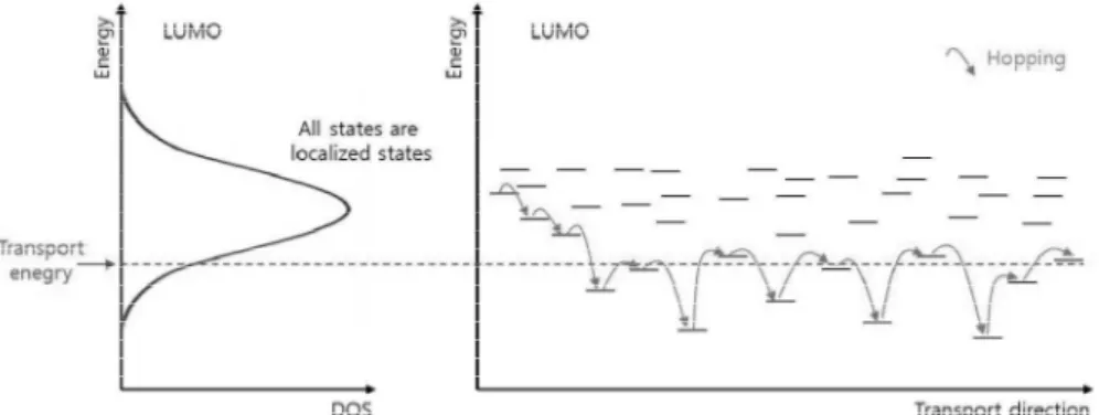
Further theory for hopping charge transport is the Gaussian disorder
model (GDM) proposed by Bassler (Bassler, 1993), and widely used for solids where the degree of disorder is high, where ‘strong localization’ results in the absence of extended band states. In this model, all electronic states have to be regarded as localized states, and their energetic distribution is described by a Gaussian distribution, Figure 4.
Figure 4: Hopping transport through the localized states in the Gaussian
disorder model (GDM).
The major characteristics of this model are the non Arrhenius temperature behavior and the dependence of the mobility on the electric field. The expression for the GDM mobility can be written as:
µ
($, ) =
µ
∞ [ ('(
)"#)'] ( √ ) (4)
where µ∞ is the high temperature limit of the mobility, σ is the energetic
disorder, related to the half-width of Gaussian DOS (density of states) and β is a factor depending on the geometric randomness arising from structural or chemical defects.
Another model commonly believed to be suitable to describe transport mechanism in organic materials is the grain boundary model that explains the trap limited currents, which are presumably caused by traps located at grain boundaries. This model uses thermionic emission and assumes that charge states at the grain boundary present an electrostatic barrier to carrier transport, but charges within the grain screen the potential, reduce the barrier and increase the effective mobility (Steudel et al., 2004), (Shang et al., 2006) and (Verlaak & Heremans, 2007). The direct correlation of potential drops and grain boundaries has been visualized with Kelvin probe microscopy
(KPM) (Ohashi et al., 2007) and phase-electrostatic force microscopy (Annibale et al., 2007). Inhomogeneous voltage drops have further be seen for slightly contaminated gate oxides with KPM, while pure SiO2 substrates
show a homogenous voltage drop of up to 85% over the channel (Luo et al., 2007). Thermionic-emission over a Schottky contact barrier has also been used to explain the temperature dependence of the charge carrier mobility in rubrene single crystals, revealing two segments supposed to be described by the intrinsic polaronic transport above 150 K and the trap-dominated conduction below, resulting in a decreasing mobility with lower temperatures (de Boer et al., 2004).
I.3.
Charge carrier injection
A physical behavior that strongly influence the amount of charge carriers injected into an organic semiconductor is the injection barrier at the metal electrodes/active layer interface. The barrier height strongly depends on the energy level matching between the Fermi level of the electrode material and the organic semiconductor energy levels, the HOMO or LUMO level of the organic semiconductor, for holes and electrons respectively.
One of the fundamental aspects of the metal/semiconductor interface is the Fermi level alignment, described by the Mott-Schottky model (Sze, 1981). When a neutral metal and a neutral semiconductor are brought in contact, the Mott-Schottky model predicts that their bulk Fermi levels align, causing the band bending in the semiconductor. In the Mott -Schottky limit, the vacuum level of the organic material and of the metal align, forming a region of net space charge at the interface, as depicted in Figure 5(a). However, the Mott-Schottky limit is rarely observed at real metal/organic interfaces due to the formation of a strong interfacial dipole ∆ between the metal surface and the organic molecules, which tends to pin the Fermi level, Figure 5(b). The origin of the interface dipole is attributed to several mechanisms; charge transfer across the interface, formation of induced or permanent dipoles into the organic layer, chemical interaction, and presence of interface states (Miozzo et al., 2010).
Figure 5: Schematic energy level diagram of the band alignment at a
metal organic interface, (a) Mott-Schottky limit vacuum level alignment, and (b) pinning of the Fermi level by induced interface states interfacial dipole.
An effective metal work function
Φ
m,eff can be defined as the differencebetween the pristine metal work function Φm and the dipole(Helander et al.,
2008),
+,,-.. = +,− / (5)
For the inorganic semiconductors, Heine (Heine, 1965) demonstrated that surface states do not exist in the forbidden gap of most of them but gap states are induced in the semiconductor as a result of the rapidly decaying tail of the electronic wave function from the metal. These metal induced gap states are independent of the energy levels in the semiconductor, and hence can either be donorlike or acceptorlike when close to the valence or conduction bands, respectively. A charge neutrality level ECNL=eΦCNL is defined as the
point at which the interface states are equally donorlike and acceptorlike. Therefore, at metal/semiconductor interfaces the charge neutrality level of the semiconductor will tend to align with the Fermi level of the metal as a result of charge transfer between the metal and the induced gap states, forming an interfacial dipole (Cowley & Sze, 1965),
+,,-.. = +012+ 34(+,− +012). (6)
Here, the interface slope parameter SΦ, for weakly interacting interfaces,
was empirically found by Mönch (Mönch, 1987) to depend on the optical dielectric constant,
34 = 1 + 0.1(891 − 1): (7) whereε∞ is the optical dielectric constant (high frequency limit of the
dielectric function). Mott-Schottky model is generally used to choose the contact metal to not limit the performances of a device because of non-ohmic contacts. In the case where the density of interface states is very high, a Fermi-level pinning can take place, and the injection barrier becomes independent on the metal workfunction: it means that contact metal has no importance for the resulting injection barriers (Koch & Vollmer, 2006). This phenomenon accounts for an important implication for organic devices: they should generally bear a substantial injection barrier that cannot vanish below a certain level determined by the position of the pinned Fermi level.
Another important aspect that can have a strong influence in charge injection, is the presence of traps at the metal/organic interface, which are mostly produced during contact fabrication (Dimitrakopoulos & Mascaro, 2001). The deposition of the metal contacts can cause local damages in the structure of the material, due to the diffusion of the deposited specie into the active layer. On the other hand, the deposition of the organic material on top of the metal electrodes can lead to an accumulation of structural defects.
I.4.
Defects in organic semiconductors
The electrical behavior of the organic materials is strongly influenced by the presence of trap states, which modify the number of the charges in the energy bands and the stability of the materials themselves. Charge carrier traps can be caused by structural defects or impurities. The structural defects are classified in: native point defects (as a vacancy), or interstitials, or extended defects (like edge dislocations, screw dislocations, or grain boundaries). Structural defects can lead to energy levels in the band gap. Some traps are electrically neutral when empty and become charged upon trapping a charge carrier. On the other hand, some defects are called antitraps because result in scattering centers, but do not cause traps (Klauk, 2006).
Organic materials are very sensitive to chemical impurities, which modify the number of the charges in the energy bands. In some cases, it is performed an artificial addition of chemical impurities which have different energy levels than the host material, and in Figure 6 is illustrated a simple scheme useful to understand the positions of electron and hole traps, respectively ;- and ;<, into a host material.
Figure 6: Representation of the energy levels of a host material with
chemical impurities (Pope & Swenberg, 1999).
In Figure 6 / ;- and / ;< represent the traps depths for electrons and holes, while (Ac)guest and (Ac)host are respectively the electron affinity of the
guest and of the host materials and (Ic)guest and (Ic)host are their ionization
energies. The electron trap depth can be approximated with the difference in electron affinity of the host and guest materials and written as (Pope & Swenberg, 1999):
/ ;-≈ (>?)@A-B;− (>?)< B; (8) In a similar way, the hole trap depth is described as:
/ ;< ≈ (C?)< B;− (C?)@A-B; (9)
However, the atoms or molecules of the added impurity may deform the host lattice due to a different size, and may change the polarizability of the lattice in local. In presence of an impurity larger than the host molecule, a compression of the lattice and an increase in polarization energy result in the host, and traps located on host molecules adjacent to the chemical impurity. On the contrary, a small polarization energy results for a smaller impurity, so that the charge transport is impeded (Pope & Swenberg, 1999).
Defects can be introduced into materials also under ambient conditions, because of the presence of light, oxygen and water. For example, the adsorbed water on the gate dielectric can dissociate and react with organic semiconductor so that water molecules are able creating hydrogen bonds retained responsible of charge transport. An example of the oxygen effect on pentacene transistor characteristics is shown in Figure 7: a transistor is
measured as grown, kept in high vacuum, and after oxygen, that is the same device was measured after the oxidation process.
Figure 7: Transfer characteristic of a pentacene transistor measured as
grown (blue line) and after oxidation (red line). The graph shows the forward and the reverse sweeps in both cases.
The characteristic oxygen effects on the transistor are a decrease in subthreshold performance, a decrease in on-current, and a shift of the transfer characteristic to more positive voltages, while the current hysteresis is essentially unaffected. Thus, these result in a decrease of the performances of the device, because the oxygen can cause changes of the flatband voltage in an organic semiconductor device. (Meijer et al., 2004), (Wang et al., 2006).
I.5.
Organic electronics today and tomorrow
Electronic devices made with organic materials are being multiple applications and have been widely commercialized. Application areas of organic electronics can be grouped into five clusters, as shown in Figure 8:
• Organic LED Lighting (OLED) • Organic Photovoltaics (OPV) • Flexible Displays
• Integrated Smart Systems (ISS, including smart objects, sensors and smart textiles).
Figure 8: Organic and printed electronics applications 6th edition of the
OE-A roadmap(2015).
Organic Display Technology and Organic light-emitting diodes (OLEDs) are commercialized in many smartphone models. For example, the Samsung Galaxy line of OLED-based smartphones occupies a significant portion of the global smartphone market. Additionally, Samsung and LG Electronics
have both announced forthcoming launches of large-screen OLED TVs. The new TVs are expected to not only be more spectacular than today’s TV technology, with respect to crisper colors and sharper contrasts, but also lighter, thinner, and more energy efficient. Organic photovoltaics (OPVs), or organic solar cells, are generally viewed as one of most exciting near-future applications of the organic electronics, not necessarily as a replacement for silicon based PVs, rather because of the unique ways that OPVs can be used due to their flexibility, large-area coverage, and low cost. Current OPV technology boasts conversion efficiencies that exceed 10 percent, reaching even 12 percent, some researchers predict organic solar cells will reach 15-20 percent efficiency. However, even at this low efficiency, very interesting potential applications can be, for example, transparent films with solar cells on mobile phones or laptops to extend battery life considerably. Organic thin film transistors (OTFTs) are considered a fundamental “building block” of modern electronic devices, as amplifying signals and as on-off switches. OFETs are also highly sensitive to specific biological and chemical agents, making them excellent candidates for biomedical sensors and other devices that interface with biological systems. By 2020, with the synthesis of even more advanced materials, electronic mobility could increase to as much as 100 cm2/Vs, while today values are at approximately 8÷11 cm2/Vs. Despite this progress, several challenges remain before OFETs will become a widespread commercial reality. For example, only recently researchers have demonstrated the fabrication of thermally stable flexible OFETs. High thermal stability is prerequisite to integrate OFETs into biomedical devices; otherwise they won’t survive high-heat sterilization. In the future vision, numerous application possibilities for everyday use will arise thanks to the consistent refinement of organic electronics. It could be possible to illuminated wallpapers for room lighting or as a variant with an imprinted TV. Windows made of transparent solar cells could provide houses with energy. Screens and laptops could be printed and rolled. This technology will continue to grow, also thanks to the possibility to integrate organic devices in many systems of other technical sectors, changing the way society interacts with technological products, and for the future organic electronics applications there are hardly any limits to the imagination.
Chapter II
Organic Thin Film Transistors
Thin-film transistor (TFT) technology was developed by Paul Weimer in the 1962, using evaporated cadmium sulfide (CdS) as the semiconductor (Weimer, 1962). These devices are a special kind of insulated-gate field-effect transistors (IGFETs) made by thin films of materials. In 1973, the first TFT liquid crystal display (LCD) was demonstrated using cadmium selenide (CdSe) transistors (Brody et al., 1973). However, mass production of this kind of LCD on large-area substrates has never been realized. Among many possible reasons, there are complications in controlling the compound semiconductor thin film material properties and device reliability over large areas. The breakthrough in the TFT concept was achieved in 1979, using plasma-enhanced chemical-vapor deposited (PECVD) hydrogenated amorphous silicon (a-Si :H) (LeComber et al., 1979). Today, a-Si :HTFTs are widely employed as the pixel drive devices in active-matrix liquid-crystal displays (AMLCDs) on glass substrates (Street, 2007). The first organic TFTs (OTFTs) were reported only in the 1980s (Tsumura et al., 1986), (Kudo et al., 1984), (Clarisse et al., 1988). An organic TFT is fabricated by depositing thin films of an active semiconductor layer as well as the gate dielectric layer and the source, drain and gate metallic contacts on the surface of an electrically insulating substrate, such as glass or plastic foil. The total thickness of the devices can be less than50 nm. In this chapter, the characteristics of organic thin transistors will be analyzed. In particular, specific attention is paid on the working principles of the OTFTs, the possible architectures, typical organic semiconductor materials used in devices, and non-ideal electrical behavior of OTFTs. Finally, a brief digression on the evolution of OTFTs is presented.
II.1.
Thin-film Transistor fundamentals
three termi (Figure 9). Figure A field transistor c applying a carriers is current ID applied bet Figure equivalent CGS, the g
and the cur
minals, named, as in a MOSFET, the source, the d .
re 9: Layer structure of an organic thin film transist ld-effect transistor operates as a voltage-controlled r controls the flow of charge between source and dr
a voltage across the gate dielectric, so that a sheet is induced in the semiconductor that allows a c
D, to flow through the semiconductor when an
between drain and source, Figure10.
re10: (a)Electrical symbol of a TFT, and (b and c)
nt circuits of a transistor, that show the gate-so gate-drain capacitance CGD, the equivalent gate
current source gm·vGS(Klauk, 2010).
e drain, and the gate
sistor.
ed current source. A drain electrodes by eet of mobile charge a current, the drain another voltage is
c) two small-signal source capacitance ate capacitance CG,
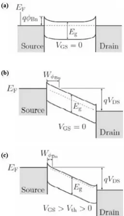
In Figure 11 is shown the behavior of the energy-level diagram across the metal/dielectric/semiconductor interface of a p-type transistor. An organic semiconductor is defined to be p-type if the Fermi level is closer to the HOMO level than to LUMO, Figure 11 (b). Symmetrically, an organic semiconductor is defined to be n-type when the Fermi level is closer to the LUMO than to HOMO. Appling a positive voltage to the metal (the gate contact), depletion mode occurs in the p-type semiconductor, Figure 11 (c), and negative charges are induced at the electrode interface between the semiconductor and the insulator. On the contrary, when a negative voltage is applied to the gate, Figure 11 (a), holes can be accumulated at the interface between the insulator and the semiconductor. Considering this structure in an OTFT, source and drain electrodes are also present, and they are in contact with the semiconductor, Figure 11: the accumulated charges at the insulator-semiconductor interface form a conductive channel between these electrodes, which allows the charges to move between source and drain by applying a bias to them.
Figure 11: Energy-level diagrams across the metal/dielectric/p-type
semiconductor interface of an organic transistor, showing (a)accumulation mode, (b) flat-band mode, (c) depletion mode.
OTFT electrical behavior is similar to a conventional FET that operates in the accumulation mode (Brown et al., 1997), Figure 12. In the semiconductor layer, the conductive channel is controlled by the gate and drain voltages, while the source electrode is grounded. The minimum gate voltage which can create the channel is called the threshold voltage, Vth. In
the p-type transistor, when the gate voltage is lower than the threshold voltage, the device is turned on and in the channel results the accumulation
of positive charges at the insulator/semiconductor interface. In a real device however, not all the charges contribute to the current due to presence of traps and defects in the materials, where the charges are trapped.
The transistor operates in "linear regime" when low drain voltage is applied and the drain current is proportional to the drain voltage, Figure 12 (a). When the drain voltage is approximately equal to the difference of the gate voltage with the threshold voltage, a depletion region next to the drain contact starts forming and the channel is pinched-off, Figure 12 (b). The reason of the formation of a depletion region is that the potential difference between the gate and the drain electrode is above the threshold voltage in this case. Further reducing the drain voltage, the drain current does not increase through the transistor, but the depletion region broadens towards the source contact, Figure 12 (c), and this operation is defined as "saturation regime". The saturation drain current can flow across the depletion region due to the high electric field in this region, which induces charge carriers swept from the pinch-off channel to the drain electrode.