Temperature Effects on the Efficiency
of Dickson Charge Pumps for Radio
Frequency Energy Harvesting
FRANCESCO G. DELLA CORTE , (Senior Member, IEEE), MASSIMO MERENDA , GENNARO G. BELLIZZI , (Student Member, IEEE),
TOMMASO ISERNIA , (Senior Member, IEEE), AND RICCARDO CAROTENUTO , (Member, IEEE)
Department of Information Engineering, Infrastructure and Sustainable Energy, Mediterranea University of Reggio Calabria, 89122 Reggio Calabria, Italy
Corresponding author: Massimo Merenda ([email protected])
ABSTRACT An experimental study is carried out to assess the effect of temperature on the conversion
efficiency of ultrahigh-frequency energy harvesters based on diode-capacitor Dickson charge pumps, fre-quently used in self-energizing circuits, such as in radio frequency identification tags or in wireless sensor nodes. Using off-the-shelf Schottky diodes often adopted for this application, it is shown that the harvester conversion efficiency at 868 MHz is temperature dependent due to the changing rectification ratio, namely the ratio between the forward and the reverse current flowing through the low barrier height Schottky diodes, which both show a positive derivative with T. The experimental study, supported by SPICE simulations, has shown that a temperature variation might be particularly harmful at the lowest incident power regimes, when even a minimal drop in the conversion efficiency might determine the out-of-servicing of a wirelessly energized circuit.
INDEX TERMS Dickson charge pump, RFID, RF-to-dc converters, temperature, UHF energy harvesting.
I. INTRODUCTION
The growing interest for the development of wireless sensors and Wireless Sensor Networks (WSNs) is strongly motivated by the huge number of new applications that they could trigger in several contexts, from intelligent living ambient to medical monitoring, from military applications to wild environment control and preservation.
In general, these devices are characterized by low bit-rates, volume constraints for the nodes and sub-milliwatts average power consumption. Their deployment is however strongly limited in many contexts by the use of electro-chemical batteries, which limits the sensor lifetime. However, the low power requirements of these devices would allow, at least in some cases, the possibility of powering the nodes by scavenging ambient power from the surroundings [1]–[8]. This can potentially extend the lifetime of a sensor to infinite duration and reduce the maintenance costs associated with battery-operated devices.
Among the most common mean of wireless energization, harvesting of energy spread around by antennas that emit radio waves at communication wavelengths is very often
used, e.g. by radio-frequency identification (RF-ID) plat-forms. In these cases, an operating distance of a few meters from the transmitting antenna is normally required, which usually translates into harvested powers that are well below 0 dBm.
An RF energy harvester generally consists of a so-called rectenna, namely a receiving antenna coupled to an ac-to-dc rectifying circuit. A simple matching network, generally con-sisting of a capacitor and/or an inductor, is often positioned between these two sections.
The core circuit of these high-frequency ac-dc converters is normally a diode-based rectifier, coupled to a low pass filtering capacitor. Instead of p-n junction diodes, Schottky diodes are by far the most preferred in these circuits for their low threshold voltage, which allows to save as much as possible of the amplitude of the input signal, and for the low parasitic capacitance, allowed by the virtually zero by-pass diffusion capacitance.
One of the most common rectifying topologies is the Dickson stage [9], a charge pump schematically shown in Fig. 1. Beside its relatively high efficiency, this circuit
FIGURE 1. Basic cell of a Dickson charge pump.
features a simple topology allowing easy multi-stage configu-ration, which is fundamental to get the desired output voltage level when dealing with very low input signals.
The performances of this simple circuit have been accu-rately studied [10]–[12], and also recently it has been considered as the main building block of high efficiency RF-DC rectifiers, either circuit board mounted or fully integrated [13], [14].
However, as already shown through simulations in [15] for a p-channel MOSFET voltage multipliers, the performances of charge-pump based RF harvesters are affected by tempera-ture. This might be particularly harmful at the lowest incident power regimes, when even a minimal drop in the conversion efficiency might determine the out-of-servicing of a node.
In this paper, we present the full experimental char-acterization of a standard Dickson harvester designed for UHF applications, operated in the temperature range from 25 C to 85 C, considering an incident RF power of -30 dBm to 0 dBm. We provide a justification of the experimental results, analyzing in particular the role of diodes, whose char-acteristics are well known to be strongly temperature depen-dent. The circuits are based on a popular Schottky diode, the HSM2852 [16], a silicon device specifically designed for small signal applications at frequencies below 1.5 GHz, commonly used for RF energy harvesting circuits mounted on printed circuit boards [13], [17]–[19]. A parallel characteriza-tion was also carried out on another commercial device [20], and the results are compared.
The paper is organized as follows: Section II describes the reference circuit used in this study, the experimental set-up and the measurement methods. Section III reports about the experimental results on the conversion efficiency and their analysis at f = 868 MHz, over the anticipated temperature and input power ranges. In Section IV, SPICE simulation results are shown for a simple configuration and compared to measurements to provide a better interpretation of the observed phenomena, while conclusions are drawn in Section V.
II. REFERENCE CIRCUIT OPERATION AND EXPERIMENTAL SETUP
When a sinewave Vi = VMsin(!t) is applied to the input
of the basic cell of a Dickson charge pump (DCP), shown in Fig. 1, the operation of the circuit can be roughly divided
in two phases: in phase 1, corresponding to the negative half-wave, capacitor C1is charged via the clamp diode D1; when
Vicrosses zero, the level of node A is therefore at a voltage
VM-VD1, where VD1 is the voltage drop on the diode D1.
During the positive semi-period of Vi (phase 2), diode D2
allows the one-way charge transfer to capacitor C2, which
charges up to the maximum voltage of 2 ⇥ VM VD1 VD2.
For the correct operation of a Dickson cell, a few rules of thumbs need to be fulfilled, among which:
1) the diodes must be low voltage drop (Vd) ones to allow
the highest output voltage;
2) they must have a low DC reverse current Irevin order to
avoid, during phase 2, a parasitic path toward ground for the charge accumulated on C1;
3) at the operating frequency of the circuit f = ! 2⇡, their
parasitic capacitances, namely the junction capacitance Cj
and the diffusion capacitance Cdiff, should provide a
negli-gible by-pass path for current;
4) the current drawn by the load R should be low enough to allow the full charging of C2.
Beside these simple rules, several others could be men-tioned, among which an appropriate RF design of the circuit and an effective impedance matching between the source (antenna) and the charge pump [21].
Requests 1 and 3 generally imply the use of silicon Schottky diodes, which are known to show a Vd as low
as 0.2 V, and Cdiff = 0 due to their inherent majority
carrier-based working principle. Request 2 would in turn call for the use of p-n junction diodes. Some (or all) of these characteristics are however more or less temperature dependent. In particular, Vd and Irev certainly are, being to
a first approximation [22]: Vd =kTq ⌘ln✓ ID Irev ◆ , (1) and Irev= AR⇤⇤T2e q'bkT , (2) where T is the absolute temperature, k is the Boltzmann constant, q is the electron charge, ⌘ is the ideality factor, IDis
the forward current, Irev the reverse saturation current, A is
the junction area, R⇤⇤is the Richardson constant and 8bis
the Schottky barrier height.
In order to highlight the effect of temperature on the perfor-mances on a DCP, experimental measurements were carried out on a 2-stage DCP circuit as that depicted in Fig. 2. For a careful interpretation of results, it should be considered that diodes are nonlinear devices, and therefore the DCP is a nonlinear circuit. It turns out that its input impedance varies with the input power, and the reflected power also varies accordingly. For this reason, an extensive set of mea-surements was carried out in this study to extract the DCP conversion efficiency calculated with respect to the net RF input power at its input end. This novel approach allows to obtain information about the quality of the rectifier regardless
FIGURE 2. Schematic of the 2-stage Dickson charge pump used for experimental measurements and SPICE simulation.
FIGURE 3. Layout of the 2-stages DCP printed circuit board from Fig. 2.
of the impedance mismatch with the RF source, e.g. the receiving antenna.
The sample charge pump was realized on a flexible 0.8 mm thick FR4 printed circuit board, with the layout shown in Fig. 3. The capacitors, with a value of 10 pF chosen in agreement with previous studies [13], [23], are low Equiva-lent Series Resistance (ESR) ones, with a maximum temper-ature coefficient of ±30 ppm/ C [24]. This stage is in fact the front-end between the antenna and other similar stages put in series to boost the output voltage. For this reason, it handles the weakest signals within a multi-stage configuration and is therefore a sort of bottleneck for the whole circuit.
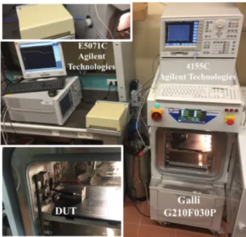
A schematic representation and a picture of the experi-mental setup are shown in Fig. 4 and Fig. 5 respectively. It consists of a Vectorial Network Analyzer (VNA – model Agilent Technologies E5071C), a Semiconductor Parameter Analyzer (SPA – model Agilent 4155C), and a controlled thermostatic oven (Galli G210F030P) for the setting of the reference temperature.
A precision 50 RF cable connects the VNA to the Dick-son harvester input via a feed-through hole of the oven. The DC output of the harvester is connected to the SPA. The VNA was properly calibrated before starting the measurements, shifting the reference plane to the input of the DCP.
FIGURE 4. Schematic representation of the experimental setup.
FIGURE 5. Experimental setup.
The measurement procedure consisted of the following steps. First, while holding the DCP output at fixed voltages (from 0 V to 2 V in steps of 100 mV), the |S11| parameter was
measured with the VNA, at 500 different input power levels, from -30 dBm to 0 dBm. This characterization is essential for a correct evaluation of the subsequent measurements. In fact, due to possible impedance mismatch and attenuations effects, the power actually delivered to the DCP, Pin,actual, will be
quantified as [25]: Pin,actual=
⇣
1 |0|2⌘Pin,feed, (3) where 0 is the reflection coefficients and Pin,feedis the power
fed by the VNA. For the used configuration, the reflection coefficient 0 is coincident with |S11|.
Afterward, the VNA RF output power, Pin,feed, was set to
20 dBm and the I-V output characteristic of the DCP was registered by the SPA. The measurement was repeated for Pin,feedin the range 20 dBm to 0 dBm, in steps of 5 dBm.
The whole set of measurements was repeated at four tem-peratures, namely 25, 45, 65 and 85 C.
Finally, by calculating, as hereafter detailed, the power actually delivered to the Dickson charge pump, Pin,actual,
the net conversion efficiency of the circuit was calculated. III. EXPERIMENTAL RESULTS
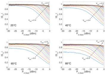
The collected values of |S11|, measured at the four
tempera-tures, are shown in Fig. 6. Each curve is obtained at a specific output voltage Vout for the DCP, from 0 V to 2 V, in steps
of 100 mV.
FIGURE 6. Collected absolute values of S11, measured at the four temperatures, for a two-stage DCP. Each curve is obtained while holding the DCP output voltage, Vout, at a fixed value, from 0 V to 2 V in steps of 100 mV.
We note that the reflection coefficient decreases with tem-perature, which means that a better coupling between the RF source and the DCP is obtained. We anticipate, however, that, in spite of the better RF coupling, the conversion efficiency of the DCP made with HSM2852 is in fact decreasing, due to the worsening of the diode characteristics and in particular of the rectification ratio.
FIGURE 7. Output I-V characteristics, measured at the four temperatures for a two-stage DCP. Measurements done at f = 868 MHz.
The measured output I-V characteristics of the DCP are shown in Fig. 7 at four temperatures and five input power
levels, Pin,feed. These curves summarize the characteristic
of the DCP seen as a dc power source. They notably recall those of a photovoltaic generator under variable illumination, and easily allow the determination of the maximum power point, i.e. the maximum power that can be delivered to a load, at each RF input power level.
In order to make clearer the effect of temperature, the superposition of the 25 C and 85 C curves is presented in Fig. 8, showing that the open circuit voltage (Voc)
remark-ably decreases as temperature increases, while the short cir-cuit current (Isc) increases.
FIGURE 8. Experimental I-V characteristics measured at the output of a 2-stages Dickson at different Pin,feedfor 25 C and 85 C (f = 868 MHz).
The above results, however, are certainly affected by the variability with the changing impedance mismatch, and consequently changing power reflection, at the input side, as anticipated in Fig. 6. As the impedance mismatch issues can be mitigated by adding a matching network [23], [26], in our work we aimed at characterizing rather the DCP circuit alone, i.e. excluding the role of the source-to-DCP coupling. The curves of Fig. 7 were therefore paired with those of Fig. 6 and data elaborated in order to highlight the tempera-ture effects on the efficiency of the charge pumping circuit. This efficiency was calculated as in (4)
⌘DCP= PPout,MPP
in,actual, (4)
where Pout,MPPis the output power at the maximum power
point and Pin,actual is the net RF power actually delivered to
the DCP circuit. The calculated ⌘DCP is reported in Fig. 9
(symbols) as a function of Pin,actual, with the solid lines
a polynomial interpolation of the calculated values. It can be seen that the conversion efficiency is strongly power dependent, dropping from 37% to zero when Pin,actual goes
from 2 to 35 dBm. Additionally, it is clearly temper-ature dependent, and gets worse as tempertemper-ature increases, especially at the lower received RF power. For example, at 20 dBm the efficiency ⌘DCP is 12% at 25 C and 4%
FIGURE 9. Measured conversion efficiency ⌘TOTof the harvester as a whole, i.e. calculated with respect to the RF power fed by the source, Pin,feed, (dashed lines), and derived conversion efficiency of the DCP alone, ⌘DCP(symbols), calculated i.e. with respect to the RF power actually delivered to the charge pump. The efficiencies are provided at four temperatures (25, 45, 65 and 85 C) and the solid lines are an interpolation of the derived ⌘DCPvalues. ⌘TOT curves at 65 C and 85 C are, in fact, coincident. Measurements done at f = 868 MHz.
power levels in RF energized systems [13], [27]–[29], it even drops to nearly zero as temperature reaches 65 C.
The same figure also reports, for comparison, the conver-sion efficiency of the whole harvester, ⌘TOT, (dashed lines)
defined as:
⌘TOT = PPout,MPP
in,feed , (5)
as a function of Pin,feed, i.e. the total power fed by the RF
source, namely the VNA. The graph shows that in this case the highest efficiency is reached at the two highest temper-atures (65 C and 85 C), although it is always well below ⌘DCP. This result implies that the power reflection at input,
which strongly degrades the harvester efficiency at all tem-peratures, in fact decreases as T increases, as already argued from Fig. 6.
A different Schottky diode type, namely the
SMS7621 [20], was considered for comparison. A 2-stage Dickson charge pump was therefore realized and character-ized, using the same setup.
A comparison between the measured efficiency of the two DCPs at three different input powers ( 25, 20, 15 dbm), and at 25 C and 85 C, is summarized in Table 1. As explained above, the reported ⌘DCP takes into account TABLE 1.Comparison of 2-stage Dickson efficiency values.
the power actually delivered to the DCP, calculated using (3) and the measured |S11|. The comparison shows that, while
the HSMS285-based DCP behaves much better than the SMS7621-based one at room temperature, the latter gains in efficiency as temperature increases. As will be shown in Section IV, in fact the SMS7621 starts from a two orders of magnitude smaller reverse saturation current at T = 25 C, and therefore the impact of temperature on its rectification ratio is lower than in HSMS285. The resulting improvement in its efficiency is therefore mainly due to the lowering with T of the diode threshold voltage in the forward bias regime.
IV. SPICE SIMULATIONS
For a better understanding of the observed phenomena, tran-sient SPICE simulations were carried out of a 2-stage Dick-son rectifier (Fig. 2), based on LTspice [30]. Vs is the RF
source (f = 868 MHz) with an internal impedance Rs =
50 . The four capacitors C1-C4 have a capacitance of 10 pF. According to the behavior shown in Fig. 6, the load is a resistor R chosen each time to have the harvester work in its maximum power point.
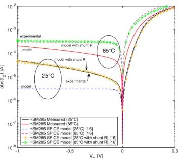
FIGURE 10. Experimental, SPICE model and SPICE model with shunt resistor Rsh, current-voltage characteristics of the HSMS285 Schottky diode used for the Dickson charge pump. The characteristics are shown at 25 C and 85 C.
In Fig. 10, the experimental I-V characteristics at 25 C and 85 C (solid line) are compared to those predicted by the simulator (dashed line), with the diode model parameters obtained from the HSMS285 datasheet [16].
The model and experiments are in good agreement for forward bias at room temperature. In particular, the pro-vided parameters do not allow to take into account the voltage dependent reverse bias current, which is instead evident in experiments. This is explained considering that, in the reverse bias region that precedes the setting up of the junction breakdown, the standard diode model assumes the reverse current constant with Vd and coincident with the
temperature-dependent saturation current Is(T ), calculated as [31]: IS(T ) = IS✓ T T0 ◆XTI N exp EG(T T0) NkTT0 (6)
where, T0 = 300 K is the parameter extraction
tempera-ture, T the actual device temperatempera-ture, and k is the Boltzmann constant. The SPICE parameter values of (6), namely the saturation current IS = 3 ⇥ 10 6 A, the saturation current
temperature exponent XTI = 2, the emission coefficient N = 1.06 and the activation energy EG = 0.69 eV, are all provided in [16]. A shunt resistor is not included in the standard SPICE model, and is therefore not provided in [16]. However, it can be introduced to account for a current slope also in reverse bias. By placing a resistor Rsh = 24 k in parallel with
the diode, a simulated characteristic very well matching the experimental one is in fact obtained both at 25 C and 85 C, in forward and reverse bias (Fig. 10). Beside this, model and experiments show a reverse current that strongly increases with T , leading soon the device to fail, at least in part, in its current blocking role during the reverse bias phases.
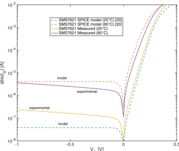
Also for the SMS7621, the experimental current-voltage characteristic and the SPICE model are in poor agreement with the datasheet model (Fig. 11), with the latter again underestimating or overestimating the current respectively at 25 C and 85 C.
FIGURE 11. Experimental and SPICE model current-voltage characteristics of the SMS7621 Schottky diode used for the Dickson charge pump. The characteristics are shown at 25 C and 85 C.
To qualitatively show the impact of the temperature depen-dent reverse bias current on the circuit conversion efficiency, the simulated periodic evolution of the voltages appearing on D3 and D4, when the RF input power at plane XX’ is
20 dBm, are shown in Fig. 12 as an example, with the load R set at 30 k, a value that allows operation at the maximum power point. It can be seen that the two diodes are cyclically biased by the same waveforms, apart from a ⇡ phase delay.
FIGURE 12. Simulated voltages across D3 and D4 according to Fig. 2 at Pin,av= 20 dBm.
Note also that that the maximum forward and reverse biases are approximately 0.22 V and 0.12 V, respectively. Now, by comparing with the experimental I-V characteristics of Fig. 10, it can be seen that the model-predicted reverse bias current at Vd = 0.12 V will increase by almost two orders
of magnitude at 85 C. This will introduce a strong leakage of the charge accumulated on the two capacitors C3 and C4 during the two phases when D4 is expected to block the back-flow of charge from C4, and respectively D3 to open the path between C and B nodes (see Fig. 2) to allow C3 boost the output voltage.
In order to show the effects of diode model quality on the simulated harvester efficiency, the Pinpower at the DCP
input (plane XX’ in Fig. 2) and that dissipated on the load R, namely Pload, were calculated by simulations at -20 dBm
for the HSMS285-based DCP. The conversion efficiencies, calculated as Pload/Pin, are reported in Table 2 at the two
tem-peratures, and compared to those obtained with experiments. At 25 C, a strong disagreement is found between simula-tions and experiments, with a simulated ⌘DCPof 51% against
the much lower measured value of 15% observed in Fig. 9. The efficiency overestimation resulting from simulations is explained with the already highlighted strongly underesti-mated reverse saturation current provided by the model and flowing through the diodes when they operate in reverse bias (Fig. 10). By including Rsh = 24 k in the diode model to
account for its leakage current, the calculated efficiency drops to a much more realistic 20%, as reported in Table 2.
TABLE 2. Simulated and experimental efficiency values.
At 85 C, in spite of the divergence between experimental and modeled currents shown in Fig. 10 without the shunt resistor, the measured and simulated efficiencies disagree
comparatively less (7% against 17%). This is due to the fact that, although at this temperature the diode model over-estimates the reverse current, with its predictable negative effects on efficiency, at the same time the forward current is also overestimated (see Fig. 10), which in turn brings positive effects on the circuit simulated behavior. Note that in this case, because of the higher reverse saturation current, the shunt resistor has no impact on the overall conversion efficiency.
A positive temperature coefficient for ⌘DCP was instead
reported in [15], where the behavior of a MOSFET-based voltage multiplier for RF energy harvesting is studied by ADS simulations. Of course, at a physical level, tempera-ture acts on MOSFETs differently than on diodes. In [15], the p-MOSFET threshold voltage Vthlinear decreases with
temperature by a factor ↵T = 0.6 mV/K, approximatively
resulting therein in a 7% increase of the normalized conver-sion efficiency for T in the range 25÷85 C. A compensation scheme for Vth was also proposed in that study to stabilize
the circuit performances, a difficult task for a diode-only based DCP.
In principle, the temperature dependence of the capac-itances C1-C4 should be also considered in simulations. However, the anticipated small temperature coefficient of ±30 ppm/ C [24] (Section II) has in fact no effects on the circuit operation and can be therefore neglected.
V. CONCLUSION
An experimental study on the effects of temperature on the conversion efficiency of Dickson charge pumps used in energy harvesting rectennas has been presented. Measure-ments were designed to exclude the role of the temperature-and power-dependent impedance matching between the source, namely the antenna, and the ac-dc converter. Supported by SPICE simulations, the experimental study has shown that temperature can have a significant impact on the circuit efficiency, in the temperature range from 25 C to 85 C. In particular, the Dickson rectifying circuit showed a different behavior depending on the used diode type. In one case (HSMS285) the conversion efficiency drops from 15% to 7% with an input power of 20 dBm, and from 7% to nearly zero at 25 dBm. On the other hand, by using SMS7621 diodes, the conversion efficiency rises, in the same temperature range, from 4% to 8% at 20 dBm, and from 0.5% to 4% at -25 dBm. It has been shown that the behavior depends tightly on the diode reverse saturation current, which is particularly high in the low-barrier Schottky diodes typically used for these applications, and moreover shows a strong temperature dependence.
REFERENCES
[1] R. Colella, L. Catarinucci, and L. Tarricone, ‘‘Improved battery-less aug-mented RFID tag: Application on ambient sensing and control,’’ IEEE Sensors J., vol. 16, no. 10, pp. 3484–3485, May 2016.
[2] S. Kim et al., ‘‘Ambient RF energy-harvesting technologies for self-sustainable standalone wireless sensor platforms,’’ Proc. IEEE, vol. 102, no. 11, pp. 1649–1666, Nov. 2014.
[3] K. W. Choi, L. Ginting, P. A. Rosyady, A. A. Aziz, and D. I. Kim, ‘‘Wireless-powered sensor networks: How to realize,’’ IEEE Trans. Wire-less Commun., vol. 16, no. 1, pp. 221–234, Jan. 2017.
[4] X. Lu, P. Wang, D. Niyato, D. I. Kim, and Z. Han, ‘‘Wireless networks with RF energy harvesting: A contemporary survey,’’ IEEE Commun. Surveys Tuts., vol. 17, no. 2, pp. 757–789, 2nd Quart., 2015.
[5] C. He, M. E. Kiziroglou, D. C. Yates, and E. M. Yeatman, ‘‘A MEMS self-powered sensor and RF transmission platform for WSN nodes,’’ IEEE Sensors J., vol. 11, no. 12, pp. 3437–3445, Dec. 2011.
[6] S. E. Adami et al., ‘‘A flexible 2.45-GHz power harvesting wristband with net system output from 24.3 dBm of RF power,’’ IEEE Trans. Microw. Theory Techn., vol. 66, no. 1, pp. 380–395, Jan. 2018.
[7] S. Hemour et al., ‘‘Towards low-power high-efficiency RF and microwave energy harvesting,’’ IEEE Trans. Microw. Theory Techn., vol. 62, no. 4, pp. 965–976, Apr. 2014.
[8] M. Pinuela, P. D. Mitcheson, and S. Lucyszyn, ‘‘Ambient RF energy harvesting in urban and semi-urban environments,’’ IEEE Trans. Microw. Theory Techn., vol. 61, no. 7, pp. 2715–2726, Jul. 2013.
[9] J. F. Dickson, ‘‘On-chip high-voltage generation in MNOS integrated circuits using an improved voltage multiplier technique,’’ IEEE J. Solid-State Circuits, vol. JSSC-11, no. 3, pp. 374–378, Jun. 1976. [10] T. Tanzawa and T. Tanaka, ‘‘A dynamic analysis of the Dickson charge
pump circuit,’’ IEEE J. Solid-State Circuits, vol. 32, no. 8, pp. 1231–1240, Aug. 1997.
[11] J. A. Starzyk, Y.-W. Jan, and F. Qiu, ‘‘A DC-DC charge pump design based on voltage doublers,’’ IEEE Trans. Circuits Syst. I, Fundam. Theory Appl., vol. 48, no. 3, pp. 350–359, Mar. 2001.
[12] G. Palumbo and D. Pappalardo, ‘‘Charge pump circuits: An overview on design strategies and topologies,’’ IEEE Circuits Syst. Mag., vol. 10, no. 1, pp. 31–45, Mar. 2010.
[13] P. Nintanavongsa et al., ‘‘Design optimization and implementation for RF energy harvesting circuits,’’ IEEE J. Emerg. Sel. Topics Circuits Syst., vol. 2, no. 1, pp. 24–33, Mar. 2012.
[14] R. Colella, M. Pasca, L. Catarinucci, L. Tarricone, and S. D’Amico, ‘‘High-sensitivity CMOS RF-DC converter in HF RFID band,’’ IEEE Microw. Wireless Compon. Lett., vol. 26, no. 9, pp. 732–734, Sep. 2016. [15] J. S. Yuan and Y. Bi, ‘‘Process and temperature robust voltage multiplier
design for RF energy harvesting,’’ Microelectron. Rel., vol. 55, no. 1, pp. 107–113, 2015.
[16] Broadcom Limited. HSM285x Datasheet. Accessed: Sep. 22, 2017. [Online]. Available: https://docs.broadcom.com/docs/AV02-1377EN [17] T. Mitani, S. Kawashima, and T. Nishimura, ‘‘Analysis of voltage
dou-bler behavior of 2.45-GHz voltage doudou-bler-type rectenna,’’ IEEE Trans. Microw. Theory Techn., vol. 65, no. 4, pp. 1051–1057, Apr. 2017. [18] D. Pavone, A. Buonanno, M. D’Urso, and F. G. D. Corte, ‘‘Design
con-siderations for radio frequency energy harvesting devices,’’ Prog. Electro-magn. Res. B, vol. 45, pp. 19–35, 2012.
[19] P. Di Marco, V. Stornelli, G. Ferri, L. Pantoli, and A. Leoni, ‘‘Dual band harvester architecture for autonomous remote sensors,’’ Sens. Actuators A, Phys., vol. 247, pp. 598–603, Aug. 2016.
[20] Skyworks SMS7621 Datasheet. Accessed: Sep. 10, 2018. [Online]. Avail-able: http://www.skyworksinc.com/uploads/documents/Surface_Mount_ Schottky_Diodes_200041AD.pdf
[21] R. E. Barnett, J. Liu, and S. Lazar, ‘‘A RF to DC voltage conversion model for multi-stage rectifiers in UHF RFID transponders,’’ IEEE J. Solid-State Circuits, vol. 44, no. 2, pp. 354–370, Feb. 2009.
[22] S. M. Sze and K. K. Ng, Physics of Semiconductor Devices. Hoboken, NJ, USA: Wiley: 2007.
[23] A. Sample, D. Yeager, P. Powledge, and J. Smith, ‘‘Design of a passively-powered, programmable sensing platform for UHF RFID systems,’’ in Proc. IEEE Int. Conf. RFID, Mar. 2007, pp. 149–156.
[24] KEMET. HiQ-CBR, Low ESR Series Capacitor Datasheet. Accessed: Jun. 14, 2018. [Online]. Available: http://www.kemet.com/Lists/ ProductCatalog/Attachments/490/KEM_C1030_CBR_SMD.pdf [25] W. C. Chew, Waves and Fields in Inhomogeneous Media. Piscataway, NJ,
USA: IEEE Press, 1995.
[26] C. Felini, M. Merenda, and F. G. D. Corte, ‘‘Dynamic impedance matching network for RF energy harvesting systems,’’ in Proc. IEEE RFID Technol. Appl. Conf. (RFID-TA), Sep. 2014, pp. 86–90.
[27] M. Merenda et al., ‘‘Performance assessment of an enhanced RFID sensor tag for long-run sensing applications,’’ in Proc. IEEE Sensors, Nov. 2014, pp. 738–741.
[28] M. Merenda, C. Felini, and F. G. D. Corte, ‘‘An autonomous and energy efficient smart sensor platform,’’ in Proc. IEEE Sensors, Nov. 2014, pp. 1208–1212.
[29] P. Di Marco, A. Leoni, L. Pantoli, V. Stornelli, and G. Ferri, ‘‘Remote sensor networks with efficient energy harvesting architecture,’’ in Proc. 12th Conf. Ph.D. Res. Microelectron. Electron. (PRIME), Jun. 2016, pp. 1–4.
[30] Analog Devices, LTspice IV, Norwood, MA, USA, 2018.
[31] P. Antognetti and G. Massobrio, Semiconductor Device Modeling With SPICE. New York, NY, USA: McGraw-Hill, 1993.
Francesco G. Della Corte (M’98–SM’15) was born in Naples, Italy. He received the M.S. degree in electronic engineering from the University of Naples Federico II, Naples, in 1988. He was with Sirti spa, CNR-IMM, ENEA, Optel-InP. He is currently a Full Professor of electronics with the Mediterranea University of Reggio Calabria, Italy, serving as a Coordinator of the M.S. Pro-gram in electronic engineering and the Head of the Microelectronics Lab. His main research topics are integrated sensors, wide bandgap semiconductor device modeling, silicon photonics, and subjects on which he authored or co-authored over 100 journal papers and holds three patents.
Massimo Merenda received the B.S., M.S., and Ph.D. degrees in electronic engineering from the Mediterranea University of Reggio Calabria, Italy, in 2002, 2005, and 2009, respectively. From 2003 to 2005, he was a fellow at IMM-CNR, Naples, Italy. He is currently a Researcher with the Department of Information Engineering, Infras-tructure and Sustainable Energy, Mediterranea University of Reggio Calabria. His research inter-ests include the design and development of appli-cation specific integrated circuits, silicon sensors, embedded systems, and intelligent radiofrequency identifiers (smart-RFID) with energy harvesting capabilities. He was a recipient of the Prof. A. Rizzo Award from the Italian Sensor Association in 2007.
Gennaro G. Bellizzi (S’15) was born in Naples, Italy, in 1992. He received the M.S. Laurea degree (summa cum laude) in biomedical engi-neering from the University of Naples Federico II in 2015. He is currently pursuing the Ph.D. degree in information engineering (applied elec-tromagnetics) with the Mediterranea University of Reggio Calabria. In 2014, he joined the Institute for Electromagnetic Sensing of the Environment Research Group, National Research Council of Italy, Naples.
He was a recipient of the IEEE Antennas and Propagation Society Doctoral Research Grant in 2017.
Tommaso Isernia (M’11–SM’15) received the Laurea (summa cum laude) and Ph.D. degrees from the University of Naples Federico II, Naples, Italy. He is currently a Full Professor of electro-magnetic fields with the Mediterranea University of Reggio Calabria, Reggio Calabria, Italy, where he serves as the Director of DIIES and the Super-visor of the LEMMA Research Group and of the Ph.D. Course on information engineering. He is also with the Consorzio Nazionale Italiano per le Telecomunicazioni Consortium, where he serves as a member of the Board of Administrators. He is also involved in field synthesis problems for biomed-ical imaging and therapeutic applications. His current research interests include inverse problems in electromagnetics with a particular emphasis on phase retrieval, inverse scattering, and antenna synthesis problems. He was a recipient of the G. Barzilai Award from the Italian Electromagnetics Society in 1994.
Riccardo Carotenuto (M’00) was born in Rome, Italy. He received the Dr.Sc. degree in elec-tronic engineering and the Ph.D. degree from the Sapienza University of Rome, Rome, in 1992 and 1997, respectively. He was with the Department of Electronic Engineering, Roma Tre University, Rome, where he was involved in ultrasonic micro-motors, resolution enhancement of echographic imaging systems, and theory and technology of capacitive micromachined ultrasound transducers. Since 2002, he has been an Associate Professor with the Department of Infor-mation Engineering, Infrastructure and Sustainable Energy, Mediterranea University of Reggio Calabria, Reggio Calabria, Italy. He has authored or co-authored over 80 papers published on international journals and con-ferences proceedings. His current research interests include indoor local-ization, ultrasound imaging, ultrasound actuators, time-series prediction, nonlinear systems identification and control, and neural networks theory and applications.