ii
Study of the electronic and structural properties of tin dioxide
and armchair graphene nanoribbons
Luis Miguel Villamagua Conza, Ph.D. University of Calabria, 2015
Supervisors: Dr. Manuela Carini Dr. Arvids Stashans
Abstract:
This dissertation is focused on the study of the electrical and structural properties of two emerging materials, the tin dioxide (SnO2) and graphene, which have attracted the
interest of the semiconductor-device community due to their extraordinary characteristics.
The SnO2 has been studied by means of ab initio simulations (Vienna ab initio
Simulation Package, VASP). Both n-type and p-type conductivities were investigated. The intrinsic n-type conductivity has been achieved through two schemes: the first one through the combination of oxygen deficiencies and interstitial atoms inside the SnO2
lattice, whereas in the second one, through the combination of interstitial and/or substitutional hydrogen atoms inside the SnO2 lattice. On the other hand, the p-type
conductivity was achieved by codoping n-type SnO2 (from earlier configurations) with
low concentrations of nitrogen and aluminum impurities. The performed theoretical studies, to a good extent, agree with the experimental results provided by our collaboration group at the National Central University, Jhong-Li (Taiwan). In prospective, these results confirmed that SnO2 is a promising candidate to replace
indium in transparent conductive oxides (TCOs) used in photovoltaic, thin-film transistor, and transparent electronic applications.
iii
The theoretical study of graphene has been conducted by means of a tight-binding approach (Atomistic ToolKit simulation package, ATK): the electrical and structural properties of edge-defected armchair graphene nanoribbons (AGNRs) were studied. It was found that Stone-Wales defect (very common in carbon allotropes) placed at the edges of the AGNRs can spark an extra opening of the energy gap in graphene, in addition to that obtained through the quantum confinement of electrons. Moreover, an experimental study on the electrical properties of graphene was carried out at the Tyndall National Institute (Ireland) to understand the influence of multiple cleaning treatments on graphene field-effect transistor (GFET) devices. Debris from residual polymers that appeared during device fabrication was swept off the graphene surface without significantly degrading the electronic properties of the graphene flake. The results suggest that the unusual but extraordinary properties of these graphene allotropes can be considered as a very innovative booster for semiconductor devices, allowing the improvement of the scaling trend beyond that obtained with conventional materials.
iv
Studio delle proprieta elettroniche e strutturali del diossido di
stagno e nanostrisce di grafene di tipo armchair
Luis Miguel Villamagua Conza, Ph.D. Universitá della Calabria, 2015
Relatori: Dr. Manuela Carini Dr. Arvids Stashans
Riassunto:
Questa tesi si focalizza sullo studio delle proprietà elettriche e strutturali di due materiali emergenti: il diossido di stagno (SnO2) e il grafene, che hanno attratto
l'interesse dei ricercatori nel campo dei dispositivi a semiconduttore grazie alle loro caratteristiche straordinarie.
Il diossido di stagno è stato studiato per mezzo di simulazioni basate su metodi ab
initio (software: Vienna ab initio Simulation Package, VASP). Entrambe le conduttività
di tipo "n" e "p" sono state indagate. La conduttività di tipo "n" è stata ottenuta attraverso due soluzioni: sia attraverso la combinazione di lacune di ossigeno e atomi interstiziali nella rete cristallina di SnO2, sia attraverso la combinazione di atomi di
idrogeno interstiziali e/o sostitutivi nella rete cristallina di SnO2. D'altra parte, la
conduttività di tipo "p" è stata ottenuta attraverso il drogaggio a bassa concentrazione con impurità di azoto e alluminio dei campioni di SnO2 precedentemente drogato di tipo
"n". Gli studi teorici effettuati sono stati in grado di prevedere a grandi linee i risultati sperimentali forniti dal gruppo della National Central University, Jhong-Li (Taiwan), con cui si è collaborato. In prospettiva, questi risultati confermano che il diossido di stagno è un candidato molto promettente per rimpiazzare l'indio in ossidi conduttivi trasparenti (transparent conductive oxides o TCO in inglese) usati per applicazioni di fotovoltaico, transistori a film sottili, ed applicazioni di elettronica trasparente.
v
Lo studio teorico sul grafene è stato condotto per mezzo del metodo tight-binding (software: Atomistic Toolkit, ATK): sono state studiate le proprietà elettriche, strutturali e di trasporto di nanostrisce del tipo armchair (armchair graphene nanoribbons o AGNR in inglese). Si è trovato che i difetti Stone-Wales (molto comuni negli allotropi del carbonio) posti ai bordi delle AGNR possono generare un aumento ulteriore della banda energetica proibita del grafene, in aggiunta a quanto ottenibile tramite il confinamento quantistico degli elettroni. Inoltre, uno studio sperimentale sulle proprietà elettriche del grafene è stato effettuato presso l'Istituto Nazionale Tyndall (in Irlanda) per comprendere l'influenza di molteplici trattamenti di pulizia su dispositivi GFT (graphene field effect transistors in inglese). I detriti da polimeri residui, apparsi durante la fabbricazione del dispositivo, sono stati spazzati via dalla superficie di grafene senza degradare significativamente le proprietà elettroniche del fiocco. Questi risultati suggeriscono che le caratteristiche atipiche ma straordinarie di questi allotropi del grafene possono sovralimentare le prestazioni dei dispositivi a semiconduttore, estendendo i miglioramenti legati alla miniaturizzazione delle dimensioni dei dispositivi elettronici al di là di quelli ottenibili con i materiali convenzionali.
vi
Acknowledgements
Writing this dissertation has been fascinating and extremely rewarding. I would like to thank a number of people who have contributed to the final result in many different ways:
First and foremost, I would like to express my special appreciation and thanks to my advisors, Dr. Manuela Carini and Dr. Felice Crupi, at the University of Calabria (Italy) for giving me the opportunity to discover the beauty of research during these three years. Without their vision, technical guidance, patience, and willingness to let me pursue this work, this dissertation would not have been possible.
Special thanks go to Dr. Arvids Stashans at the Technical University of Loja (Ecuador) and Dr. Aidan Quinn at the Tyndall National Institute (Ireland) for allowing me to do my internship and work placement in the groups they lead, “Fisicoquímica de materiales” and “Nanotechnology”, respectively. I greatly appreciated their contributions in time, ideas, funding and feedback on my work.
I am also grateful to all of the staff, students and interns in the groups to which I belonged during my Ph.D. pursuit. In particular, to Leonardo Renteria, Leticia Vaca, Luana Gammetta, Patrizia Notaro, Mara Vigna, Natalia Altomari, Francesco Chiaravalloti, Sebastiano Strangio, Frank Maldonado, Richard Rivera, Freddy Marcillo, Roxane Puicervert, and Daniel Lordan. Many thanks for the time you shared with me at work, and also for supporting me during difficult personal situations.
Special thanks go to Vena Pearl Boñgolan at the University of Philippines (Philippines), and Mark Lans at Radio Esperanza (Ecuador) for their helpful corrections and insightful suggestions made on this manuscript.
Last but not least, I am, and ever will be indebted to my family. Only God knows where I’d be without them. With no right to expect such support, I am deeply appreciative of their continued encouragement. ¡Un millón de gracias!
vii
Thanks, Grazie, Gracias, Yupaychani, Go raibh maith agat, Salamat.
viii
“The first obligation of all human beings is to be happy. The second obligation is to make others happy.”
ix
Dedication
I dedicate this dissertation to God, my parents, brothers and sisters (Maritza, Norman, Lorena, Vanesa, and Wilmer), and to my nephews and nieces (Maria, Jorge, Santiago,
Ana, Antonio, Santiago, Ariana, Fernando and the ones on the way).
I realized that by having you by my side, I have always had everything one person needs to be happy and successful in life. Thank you for the encouragement and support
that you provided me with in my Ph.D. pursuit.
x
Table of Contents
Abstract:... ii Riassunto: ... iv Acknowledgements ... vi Dedication ... ix Table of Contents ... xList of abbreviations ... xii
List of symbols ... xiv
Chapter 1. Introduction ... 1
1.1. Motivation ... 1
1.2. Scope of the dissertation ... 3
1.3. Dissertation outline ... 3
Chapter 2: Basics of SnO2 ... 5
2.1. Introduction ... 5
2.2. Crystalline lattice ... 6
2.3. Band structure and density of states ... 7
2.4. Electrical properties ... 9
2.5. Parametrization of SnO2 into VASP ... 12
Chapter 3. Basics of carbon allotropes ... 14
3.1. Introduction ... 14
3.2. The direct and reciprocal lattice ... 15
3.3. Tight-binding description of graphene ... 16
3.4. Carbon allotropes ... 19
3.5. Graphene nanoribbons ... 20
3.6. Parametrization of the AGNRs into Atomistic Toolkit ... 22
Chapter 4. Discussion of results ... 24
4.1. Introduction ... 24
4.2. Origin of the intrinsic n-type conductivity in SnO2... 25
4.2.1. First scheme to achieve n-type conductivity in SnO2 ... 25
4.2.2. Second scheme to achieve n-type conductivity in SnO2 ... 29
4.3. Transition of the conductivity in SnO2 from n-type to p-type... 34
xi
4.5. The influence of multiple cleaning treatments on CVD transferred GFET
devices ... 45
Chapter 5. Summary and conclusions ... 52
5.1. Summary ... 52
5.2. Conclusions for SnO2 ... 54
5.3. Conclusions for graphene and AGNRs ... 54
References ... 56
Appendices ... 70
Appendix A: POSCAR files ... 71
Appendix B: Fabrication of GFET devices ... 80
Appendix C: Publications in journals ... 83
Appendix D: Conference talks ... 83
Appendix E: Conferences attended ... 83
Appendix F: Summer schools attended ... 83
xii
List of abbreviations
AFM Atomic force microscopy AGNR Armchair graphene nanoribbon BZ Brillouin zone
CB Conduction band
CMOS Complementary metal oxide semiconductor
CNT Carbon nanotubes
CVD Chemical vapor deposition DFT Density functional theory
DI Deionized
DOS Density of states FET Field effect transistor FLG Few layers graphene FPD Flat-panel displays FTO Fluorine-doped SnO2
FWHM Full-width-at-half-maximum GNR Graphene nanoribbons
GGA General gradient approximation HOMO Highest occupied molecular orbital IR Infrared
ITO Indium tin oxide
ITRS International technology roadmaps for semiconductor I-V Current-Voltage
LCD Liquid-crystal display LED Light-emitting diode
LUMO Lowest unoccupied molecular orbital NP Neutrality point
OAA Optically active area
OLED Organic light-emitting diode OPV Organic photovoltaic
PDOS Partial density of states PV Photovoltaics
xiii
QED Quantum electrodynamics QHE Quantum Hall effect
RMS Root-mean-squared
S-W Stone-Wales defect TB Tight-binding
TCO Transparent conductive oxide TCE Transparent conductive electrode TFT Thin-film transistor
UV Ultraviolet VB Valence band
ZGNR Zigzag graphene nanoribbon 0-D Zero dimensional
1-D One dimensional
2-D Two dimensional
2DEG 2D electron gas 3-D Three dimensional XRX X-ray Diffraction
xiv
List of symbols
Al Aluminum cm Centimeter cm3 Cubic centimeter C Carbon °C Centigrade eV Electron-volt E Electric field EF Fermi level Eg Band gap F Fluorine J Current density H Hydrogen/Hamiltonian operator Hi Interstitial hydrogenHsub Substitutional hydrogen
Id Drain current
IOFF Off-state current or leakage current
ION On-state current or drive current
K Boltzmann constant
m Meter
mm Millimetre
n Free electron concentration/electron carrier density
N Nitrogen
Na Number of dimer lines of an AGNR
nm Nano-meter
p Free hole concentration
Rs Sheet resistance
Sn Tin atom
Sni Interstitial Sn atom
SnO2 Tin dioxide
TiO2 Titanium dioxide
O Oxygen
xv
Sni Tin interstitial
Vo Oxygen vacancy
ZnO Zin oxide
Ω Ohm
σ Electrical conductivity
Å Armstrong
ρ Electrical resistivity
τ Mean free path
T Temperature
μ Carrier mobility
Chapter 1. Introduction
1.1. Motivation
Materials that possess both optical transparency and good electrical conductivity (Villamagua, Stashans et al. 2015) form the basis of numerous important applications in contemporary and emerging technologies (Hoel, Mason et al. 2010, Stadler 2012). To name a few, photovoltaics (PV), flat-panel display (FPD), thin-film transistor (TFT) and light-emitting diode (LED) applications in energy and information technologies (Hoel, Mason et al. 2010, Ellmer 2012). This peculiar form of conductivity is usually possible in 4d metal oxides (SnO2, In2O3, CdO (Facchetti and Marks 2010)) which are widely
known as transparent conductive oxides (TCOs) (Minami 2005, Minami 2008).
In particular, Sn-doped In2O3 thin films [In2-xSnxO3:ITOs] and some of their mixtures
have proven to perform better than the other TCOs (Hoel, Mason et al. 2010, Ellmer 2012), exhibiting transparency of greater than 80% in the visible range of the spectrum and metallic conductivity of ~10-4 Ω-1cm-1 at room temperature (Godinho, Walsh et al. 2008, Minami 2008). For this reason, the indium component of the TCOs used in
2
transparent electrodes (TE) employed in the fabrication of liquid-crystal displays (LCDs) constitutes the largest use of this material (Minami 2008, Minami 2008). In addition to this niche, indium has found use in alkaline batteries (Mideen, Ganesan et al. 1989, Glaeser 1993) and thin-film solar cells (Minami 2008, Stadler 2012), notably expanding its current demand. Thus, it is widely believed that a shortage of material may occur in the near future because of the limited nature1 of world indium reserves (Minami 2008).
As a consequence of this foreseen shortage, the price of this material has been enduring a considerable increase in the last decade (Minami 2008, Hoel, Mason et al. 2010). For instance, the price of indium metal was steady at $72/kg before 1960 when its major usage was in solder alloys (Hoel, Mason et al. 2010). After 1970 the price fluctuated erratically and eventually rose to $946/kg by 2005 followed by a decline to $685/kg for 2008. The current price for indium is roughly $800/kg (RotoMetals 2015). The search for novel indium-free materials with excellent TCO characteristics is therefore a crucial goal in future optoelectronic and electronics applications (Wang, Zhi et al. 2008).
Motivated by these requirements of transparent conductive and flexible technologies, the scientific community has been envisioning new solutions to eliminate or (in the worst-case scenario) reduce the use of indium in TCOs (Minami 2008). Reduced-indium TCOs such as ZnO-In2O3, ITO-In4Sn3O12, and ZnIn-Sn-O multicomponent
oxides are attractive candidates to reduce the use of indium by approximately half (Minami 2008, Minami 2008). The best solution, however, should be the improvement of current indium-free TCOs, for example throughout the use of SnO2:x, ZnO:x, TiO2:x
semiconductors or through the use of new materials, such as graphene and some of its allotropes2 (Ellmer 2012, Torres, Roche et al. 2014).
1 The worldwide production in 2005 was 500t, which composes approximately 8% of the total estimated
reserve base Hoel, C. A., T. O. Mason, J.-F. o. Gaillard and K. R. Poeppelmeier (2010). "Transparent Conducting Oxides in the ZnO-In2O3-SnO2System." Chemistry of Materials 22(12): 3569-3579..
2 Graphene, graphene nanoribbon, graphene nanotubes, bulkyballs, nanohorns, schwarzite crystals etc
Torres, L. E. F., S. Roche and J.-C. Charlier (2014). Introduction to graphene-based nanomaterials: from electronic structure to quantum transport, Cambridge University Press.
3
1.2. Scope of the dissertation
The scope of this dissertation is to investigate the electrical, electronic, structural and/or transport properties of two emerging materials, tin dioxide (SnO2) and graphene.
With the help of the collected data in this work, obtained through quantum-mechanical simulations (density functional theory (DFT) and tight-binding theory (TBT)) and experimental measurements (Raman, X-ray photoelectron spectroscopy (XPS), atomic force microscopy (AFM), among others, provided by our collaboration group in Taiwan and Ireland), some current issues of these materials have been studied. Namely: (i) the origin of the n-type conductivity in SnO2, (ii) the n-to-p conductivity transition in SnO2,
and (iii) band gap engineering (opening) of graphene.
The n-type conductivity in SnO2 was achieved throughout two solutions: the first one
through the combination of oxygen deficiencies and interstitial atoms inside the SnO2
lattice, whereas in the second one, through the combination of interstitial and/or substitutional hydrogen atoms inside the SnO2 lattice. The p-type conductivity was
achieved by codoping n-type SnO2 (from earlier configurations) with low
concentrations of nitrogen and aluminum impurities. On the other hand, Stone-Wales (SW) defects placed at the borders of the GNRs are studied in order to understand the way in which the bandgap and therefore conductivity of graphene can be opened. The influence of multiple cleaning treatments on CVD (chemical vapor deposition) transferred GFET (a field-effect transistor (FET) using graphene as the channel material) devices was also investigated.
Based on the trend and results obtained in this work, the author strongly believes that these two materials in combination with enhancements of current recycling techniques can be the ultimate solution to indium scarcity problem, opening new frontiers in electronics and optoelectronics (Wager 2003, Georgiou, Jalil et al. 2013).
1.3. Dissertation outline
This dissertation is organized as follows:
Chapter 2 covers the basic theory of the SnO2 crystal. Therein, the electrical and
structural properties of this material will be reviewed. At the end of the chapter, the DFT parametrization in VASP will also be described. Then, chapter 3 will elaborate the
4
fundamental theory of graphene and the other sp2 allotropes, with focus on the structural and electronic properties of graphene nanoribbons (GNRs). The TB parametrization in ATK will be detailed at the end of this chapter. Moving on, in chapter 4, a thorough description and analysis of the results obtained for the two herein studied materials will be reported. Finally, chapter 5 ties together and synthesizes the various issues raised in the discussion sections, and based on the evidence accumulated until then, the conclusions will be drawn. Direction and areas for future research also will be provided in this chapter.
Chapter 2:
Basics of SnO
2
2.1. Introduction
In recent years, great interest has been focused on SnO2 owing to its importance in
gas sensing, catalysis, and solar cells applications, at both the industrial and research level (Jarzebski and Marton 1976, Villamagua, Stashans et al. 2015). SnO2 is a TCO
material, which exhibits contradictory properties of high metallic conductivity (due to native point defects) with nearly complete, insulator-like transparency in the visible range (due to its ~3.6 eV wide-band-gap) (Jarzebski and Marton 1976, Hossain, Jennings et al. 2011). In addition to these properties, SnO2 is non-toxic and displays
excellent chemical- and thermal stability (Edwards, Porch et al. 2004). Therefore, the scientific community is currently considering SnO2 as the prototype transparent
conductor material to replace expensive ITOs (Gordon 2000, Fortunato, Ginley et al. 2007). A better understanding and control of both n- and p-type conductivity in SnO2
would enhance its performance in existing applications and enable new ones, such as optoelectronics and transparent electronics.
6
In the first part of this chapter, it will be elaborated the basic theory of SnO2 crystal.
Following, it will provide a survey of its electrical and structural properties. Then, a review of the origin of the n-type conductivity and the possibility to achieve stable p-type conductivity in SnO2 will be presented. The chapter concludes with a description
of the computational method employed in the present study.
2.2. Crystalline lattice
Tin dioxide is an anisotropic polar crystal, which exhibits the tetragonal rutile structure with space group D144h or – in another notation – P42/mnm (Wyckoff and Wyckoff 1960, Svane and Antoncik 1987). Its unit cell contains six atoms, two tins (cations Sn4+) and four oxygens (anions O2−), whose atomic positions are determined by the c/a ratio and the internal parameter u. The cations are located at positions (0,0,0) and (½; ½; ½), while the anions at ±(𝑢, 𝑢, 𝑜) or ±(½ + 𝑢, ½ − 𝑢, ½). Each cation has two anions at a distance of √2𝑢𝑎 (2.053 Å) and four anions at [2(½ − u)2+ 2(c/2a)2]1/2 (2.597 Å). The lattice parameters are 𝑎 = 4.737 Å and 𝑐 = 3.185 Å (c/a
ratio is 0.673), while the internal parameter 𝑢 = [1 + 1/2(𝑐/𝑎)2](~0.307) (Svane and
Antoncik 1987). The ionic radii for O2− and Sn4+ are 1.40 and 0.71Å, respectively (Jarzebski and Marton 1976).
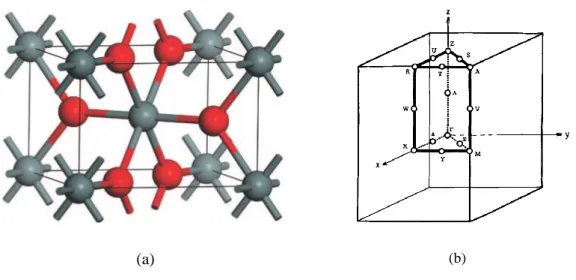
(a) (b)
Figure 2.1. (a) Unit cell of rutile SnO2 (taken from (Godinho, Walsh et al. 2008)) and (b) its reduced lattice in the BZ (taken from (Arlinghaus 1974)). Red atoms are oxygen and gray atoms are tins, respectively.
7
Following this convention, each tin atom is at the centre of six oxygen atoms placed approximately at the corner of a regular (slightly deformed) octahedron. Every oxygen atom is surrounded by three tin atoms placed approximately at the corner of an equilateral triangle. Thus, the structure is said to have a 6:3 coordination. The structure of SnO2 and its corresponding Brillouin zone (BZ) are depicted in Figure 2.1.
2.3. Band structure and density of states
The energy band structure calculated by Mishra et al. in (Mishra, Johnson et al. 1995) for the pure SnO2 is depicted in Figure 2.2 as a plot of the energy levels along the
lines of high symmetry in the BZ. Due to the large number of valence electrons in its unit cell, the band structure turn out to be very complicated.
Figure 2.2. The energy band structure of SnO2 is depicted as a plot of the energy levels along the lines of high symmetry in the BZ. The Fermi level is at the zero of the energy scale. Taken and adapted from (Mishra, Johnson et al. 1995).
One important feature to notice is that the maximum of the valence band (VB) is located at the R point on the BZ whereas the minimum of the conduction band (CB) is
8
at the Γ point. The lowest-energy interband transition is a Γ→ Γ transition (3.7 eV). The theoretical results from Mishra et al, which displays similar features to those reported in (Svane and Antoncik 1987, áLe Blevennec 1997), are inconsistent with some experimental results where the minimum direct band gap is believed to correspond to a dipole-forbidden transition at the Γ-point. The experimental minimum band-gap magnitude varies from 2.25 to 4.4 eV depending on the sample purity (áLe Blevennec 1997). Another important feature to notice is that the CB exhibits significant free-electron-like character in the Γ→Z and Γ→X directions3.
Figure 2.3. DOS of pure SnO2. The first column shows the total density of states. The following columns contain the partial densities and consecutively, the s-, , and d-like partial DOS of Sn and the s- and p-like DOS of O. Taken from (Mishra, Johnson et al. 1995).
3 Cone-like shape (also known as Dirac cone) in the band structure of materials implies that charge
9
The partial density of states (PDOS) pattern of SnO2 (Figure 2.3) indicates that a
large contribution of Sn(s)-states is found at the bottom of the valence band between -7 and -5 eV. From -5eV to the top of the valence band, the Sn(p)-states contribution decreases while the Sn(d)-states contribution increases. A large and extended contribution of the O(p)-states is also found in the valence band. Clearly, bonding between the Sn and O is dominated by the p-states of the latter.
The CB shows a predominant contribution of Sn(s)-states up to 8 eV. For energies larger than 8 eV a contribution of Sn(p)-states is found to be large. The extended O(p) contribution is minimum. More information on the band structure of SnO2 can be found
in (Svane and Antoncik 1987, áLe Blevennec 1997) and references therein.
2.4. Electrical properties
Research on SnO2 has been going on since 1910 (Chen, Pan et al. 2014) from both
experimental and theoretical standpoint (Godinho, Walsh et al. 2008, Borges, Scolfaro et al. 2010). Consequently, many of its electrical, optical, magnetic, and structural properties are widely comprehended (Jarzebski and Marton 1976, Jarzebski and Marton 1976). For example, it is known that SnO2 in its stoichiometric form (perfect
crystallographic form) manifests an insulator behaviour (Varea 2007, Godinho, Walsh et al. 2008). It is also known that nominally pure4 SnO2 (or as grown SnO2) is an n-type
wide-band-gap (3.6–4.2 eV) (Oviedo and Gillan 2000, Ji, Zhang et al. 2013) semiconductor with optical transparency of up to 97% in the visible range (Ji, Zhang et al. 2013). The resistivity of this material (10-4 - 106 Ω·cm (Manifacier, De Murcia et al. 1977, woo Lee, Kim et al. 2001)) is considerably lower than that of most semiconductors (10-3-109 Ω·cm) (Kılıç and Zunger 2002). Furthermore, nominally pure SnO2 has a carrier density (n) of up to 1020 cm-3 (Jagadish and Pearton 2011) which is
comparable to that of semimetals (1017–1020 cm-3) (Kılıç and Zunger 2002). This peculiar conducting-transparent behaviour occurs in just a few systems (Chen, Bagnall et al. 1998) such as the 4d metal oxides (SnO2 and In2O3, CdO), being thus the rarest
form of conductivity.
10
The causes for the presence of the high unintentional conductivity in nominally pure SnO2 are still unclear (Singh, Janotti et al. 2008, Ji, Zhang et al. 2013). On the one hand,
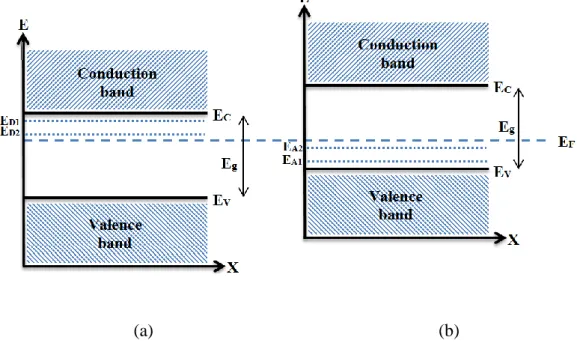
the intrinsic ability of this material to conduct electrons has been often attributed to the presence of unintentionally created donor centres, usually identified as metallic interstitial (Sni) or oxygen vacancies (Vo) that produce shallow donor levels near the CB
edge (Figure 2.4a) (Coutts, Mason et al. 1999, Ji, Zhang et al. 2013). These energy levels, which are located at around 30 and 150 meV below the CB, create only far-infrared (Drude-like) absorption, leaving the fundamental, across-the-gap absorption intact, i.e., the material remains optically transparent (Samson and Fonstad 1973, Kılıç and Zunger 2002). This stoichiometric deviation scenario (SnO2-x) is in agreement with
some experimental results, where: (i) high-purity samples display high resistivity (Gordon 2000) and (ii) the conductivity of the samples vary inversely with the oxygen partial pressure (Nagasawa and Shionoya 1971, Singh, Janotti et al. 2008).
(a) (b)
Figure 2.4. A schematic band diagram of the SnO2 endowed of n/p-type conductivity. Donor/acceptor levels (ED1 and ED2 /EA1 and EA2) are located below/above the CB/VB.
However, as widespread as this oxygen vacancy scenario is, this model raises the following question: given that vacancies usually form deep (nonconductive) levels in the band gap of both insulators (alkali halides, SiO2) and semiconductors (Si and GaAs)
11
Singh et al. (Singh, Janotti et al. 2008) have put forward a new scenario to answer this question. According to their article, hydrogen atom (H), which is commonly present in (and difficult to exclude from) the various growth and processing environments, is a likely cause of the intrinsic conductivity exhibited in nominally pure SnO2.
Native electrical properties of SnO2 is usually enhanced through extrinsic aliovalent
doping (Godinho, Walsh et al. 2008), e.g., with fluorine (F) (woo Lee, Kim et al. 2001, Wu, Liu et al. 2015) and antimony (woo Lee, Kim et al. 2001, Ji, Zhang et al. 2013) at anion and cation sites, respectively. F dopant has also been used, in fact this element has been particularly preferred to antimony because it produces the highest transparency and conductivity (Gamard, Jousseaume et al. 1999). Accordingly, thinfilms of F-doped SnO2 (FTO) are within the most used TCO materials nowadays (Gamard, Jousseaume et
al. 1999). Other dopants, such as tantalum, niobium, platinum, etc., are under investigation as well.
Moreover, despite the increasing attention put on the field of transparent electronics by the scientific and industrial communities (Singh, Janotti et al. 2008), its success depends on the ability to change the intrinsic n-type conductivity into p-type. This transition of conductivity in one single material will, in turn, bring about the long-sought transparent n-p junction (Villamagua, Stashans et al. 2015, Wu, Liu et al. 2015). The ambipolar behaviour in SnO2 could lead to applications such as ultra violet
(UV)-solar cells (Wu, Yoo et al. 1999, Liu, Hsieh et al. 2012), new generation display technologies (UV solid-state light emitting diodes (Leem, Song et al. 2004, Hossain, Jennings et al. 2011)), and ‘‘functional’’ windows, which transmit in the visible portion of the solar spectrum, yet generating electricity by absorbing in the UV region (Ni, Zhao et al. 2009).
Research on p-type conductivity in SnO2 has begun only recently (Liu, Hsieh et al.
2012, Villamagua, Stashans et al. 2015) such that achieving reproducible high quality p-type material through doping (produce energy levels just above the top of the valence band by introducing acceptor defects into the n-doped SnO2 lattice (shown in Figure
2.5b)) still poses challenges (Singh, Janotti et al. 2008). For instance, the doping level required to convert native n-type samples into p-type ones is very high (>15%) (Liu, Hsieh et al. 2012, Wu, Liu et al. 2015). Various cation dopants, such as Ga, Al, Sb, In, Zn, Fe, Co, and Li have been investigated in the last years (Liu, Hsieh et al. 2012).
12
These studies reveal that high doping concentrations (1021 - 1023 cm-3) produce low hole concentration (1015 - 1019 cm-3) (Ji, He et al. 2003, Huang, Ji et al. 2007).
Many research groups claim that the difficulty of changing the SnO2 conductivity
from n-type to p-type resides in the high concentrations of dopants required for the change to take place (Kawazoe, Yanagi et al. 2000, Liu, Hsieh et al. 2012). In case of the In-doped SnO2, at least 20 mol% impurity concentration is required to achieve
p-type electrical conductivity (Ji, Zhao et al. 2006). High impurity doping rates do not decrease even in In- and Ga-codoped samples in order to obtain required electrical behaviour, i.e. 20 mol% doping rate has to be maintained for both impurities (Mao, Ji et al. 2010). Li-doped SnO2 materials obtained by spray pyrolysis technique are claimed to
show p-type conductivity at 15 mol% of Li but 25 mol% of Li doping rate is preferred if one to obtain stable and lasting p-type samples (Bagheri-Mohagheghi and Shokooh-Saremi 2004). Investigation on Al-doped tin dioxide even argues that below 12.05 mol% of Al, the SnO2 materials have n-type electrical conductivity (Ahmed, Khan et al.
2006). Recently carried out advanced DFT computations using hybrid functionals arrive to the conclusion that all p-type impurities considered in the SnO2 lead to the localized
hole polarons being centred on anion sites and as a consequence cannot produce p-type conductivity in SnO2 (Scanlon and Watson 2012). Generally, very high concentrations
of dopants entail instability and loss of the stoichiometry of the crystal, which in turn results in the degradation of its TCO properties.
The author has recently completed theoretical calculations (presented in chapter 4) based on density functional theory (DFT) within the general gradient approximation (GGA) to delve into both the n-type and p-type conductivity in SnO2. It was studied (i)
the origin of the n-type conductivity in SnO2 from both (abovementioned) approaches
and (ii) the conductivity transition from n-type to p-type in SnO2 by co-doping the
material with small quantities of N and Al.
2.5. Parametrization of SnO
2into VASP
The numerical simulations were carried out by means of VASP (Kresse and Furthmüller 1996). The code allows to implement first-principles DFT calculations within the generalized gradient approximation (GGA) using the exchange–correlation term according to Perdew–Burke–Ernzerhof (Perdew, Burke et al. 1996). The
13
interaction between the core electrons and the valence electrons was schemed through the projector augmented wave (PAW) pseudo-potential method proposed by Blöch (Blöchl 1994) and adapted by Kresse and Joubert (Kresse and Joubert 1999). The following valence configurations have been exploited here: 4d105s25p2 for Sn, 2s22p4 for O, 2s22p3 for N, 3s23p1 for Al, and 1s1 for H atoms, respectively.
Any technique based on the DFT-GGA experiences considerable difficulties when trying to achieve a correct description of the Eg for highly correlated materials, such as
the case of SnO2. One way to minimize this error is by including an intra-atomic
interaction term for the strongly correlated electrons by an unrestricted Hartree–Fock (UHF) approximation, resulting in the so-called DFT + U approximation. By means of this additional U-term we widen the band-gap width by shifting the valence band (VB) downwards and the conduction band (CB) upwards. The U value and the lattice parameters, a and c, used throughout this work are 4.0 eV, 4.73 Å and 3.16 Å, respectively. These values were computed by our group previously and are detailed elsewhere (Stashans, Puchaicela et al. 2014).
A cut-off kinetic energy of 480 eV was used by converging the total energy to less than 1 meV/atom. The Γ-centred Monkhorst–Pack (MP) grid scheme with a 0.035 Å-1
separation was applied which corresponds to a k-point mesh of 6 x 6 x 8 for the 6-atom primitive unit cell. These parameters, also detailed in (Stashans, Puchaicela et al. 2014), were obtained through the atomic relaxation until all the forces were <0.008 eV/Å and equilibrium state of the system was achieved.
The 6-atom primitive unit cell was expanded sixteen times (2 x 2 x 4 extension), which resulted in a 96-atom supercell and a corresponding k-point mesh of 3 x 3 x 2 was adopted to maintain the same MP grid with a 0.035 Å-1 separation in the reciprocal space. All simulations were done using the 96-atom periodic supercell model.
Chapter 3.
Basics of carbon allotropes
3.1. Introduction
A great interest has aroused in both scientists and technologists toward carbon allotropes since 2004 due to their extraordinary characteristics (Wang, Zhi et al. 2008). That year, Andre Geim and Kostya Novoselov at University of Manchester isolated graphene (single-atom-thick crystallites from bulk graphite) for the first time and studied the field-effect properties of the samples (Novoselov, Geim et al. 2004). Research on graphene has shown that this material possesses: induced superconductivity (Uchoa and Neto 2007, Profeta, Calandra et al. 2012), anomalous quantum Hall effect (Greiner 1985, Zhang, Tan et al. 2005), ultrahigh electron mobility (104 cm2V-1s-1 at room temperature) (Chauhan and Guo 2010, Schwierz 2010, Deepak, Manoharan et al. 2011) and high transparency (>97% at room temperature). These characteristics have postulated the allotropes as promising materials for a wide range of nanoscience and nanotechnology applications (Geim and Novoselov 2007), such as gas sensors (Cheng, Li et al. 2010, Deepak, Manoharan et al. 2011), photovoltaics, and high-performance transistors (Chauhan and Guo 2010, Schwierz 2010). In particular,
15
graphene-based transistors have developed quickly and are now considered an option for post-silicon electronics (Schwierz 2010).
In this chapter it will be elaborated the fundamental theory of graphene and the sp2 allotropes, mainly focusing on the structural, electronic and transport properties of graphene and graphene nanoribbons (GNRs). At the end of this chapter, a description of the computational method employed in the present study will be provided as well.
3.2. The direct and reciprocal lattice
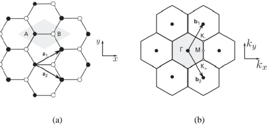
Graphene is a two-dimensional (2D) allotropic form made of sp2-hybridized carbon atoms (Novoselov, Geim et al. 2004, Dubois, Zanolli et al. 2009), periodically arranged in an infinite hexagonal —often known as the honeycomb— network (Figure 3.1a) (Bruce, O'Hare et al. 2011, Wong and Akinwande 2011). Carbon atoms are located at the vertices of the hexagons in the graphene plane (Torres, Roche et al. 2014) and its structure belongs to one of the five 2D Bravais lattices called the hexagonal (triangular) lattice (Terrones, Botello-Méndez et al. 2010). Graphene structure can be described with a basis of two non-equivalent C atoms (A and B in Figure 3.1a) per unit cell. The primitive unit cell of the underlying Bravais lattice can be considered an equilateral parallelogram (shaded gray in Figure 3.1b) with side 𝑎 = √3𝑎C−C = 2.46 Å. The
carbon-carbon bond length (𝑎C−C) is equal to 1,42Å.
(a) (b)
Figure 3.1. Basis vectors in the hexagonal lattice of graphene (a) and its corresponding Brillouin zone (b). Taken from (Torres, Roche et al. 2014)
16
The primitive unit vectors (a1, a2), as defined in Figure 3.1a, are:
𝐚𝟏= 𝑎 (√32 ,12), and 𝐚𝟐= 𝑎 (√32 , −12),
It is important to note that each A- or B-type atom is surrounded by three atoms of the opposite type (Semenoff 1984).
By using the condition 𝐚𝒊. 𝐛𝒋 = 2πδ𝑖𝑗, the reciprocal lattice vectors (b1, b2), shown in Figure 3.1b, can be obtained through:
𝐛1 = 𝑏 (12,√32), 𝐛2 = 𝑏 (12, −√32)
with 𝑏 = 4𝜋/3𝑎𝑐𝑐 = 4𝜋/𝑎√3. The first BZ in the reciprocal space is shown in Figure 3.1b (shaded gray). Out of its six corners, two of them are inequivalent (the others can be written as one of these two plus a reciprocal lattice vector). These two special points are denoted with 𝐾+ and 𝐾−. The other high symmetry point is the one
labeled with 𝑀. These symmetry points, widely known as the Dirac points, can be chosen as (Dubois, Zanolli et al. 2009, Pati, Enoki et al. 2011):
𝐊+ = 4𝜋 3𝑎( √3 2 , − 1 2) , 𝐊− = ( √3 2 , 1 2) , 𝐌 = 2𝜋 √3𝑎(1,0)
These points play an important role when studying the electronic properties of graphene (Cooper, D’Anjou et al. 2012).
3.3. Tight-binding description of graphene
The electronic structure of carbon allotropes fully engages to the hybridization (sp1,
sp2, sp3) of the constituting atoms and their arrangement within the lattice (Dubois,
Zanolli et al. 2009, Cooper, D’Anjou et al. 2012). In graphene (sp2
-hybridized carbon), among the four valence orbitals of carbon (the 2s, 2px, 2py and 2pz orbitals), the s, px,
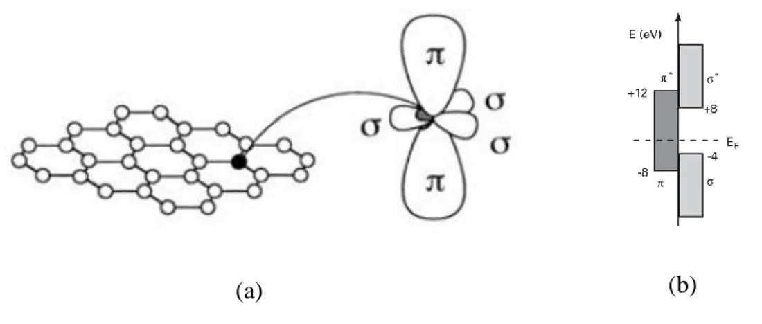
and py orbitals combine to form the in-plane σ (occupied) and σ∗ (unoccupied) orbitals
(Dubois, Zanolli et al. 2009). Such orbitals are even with respect to planar symmetry (Figure 3.2a). The σ bonds are strong covalent bonds, responsible for the elastic properties of graphene (and the other allotropes) (Dubois, Zanolli et al. 2009, Wolf 2014). The remaining pz orbital, pointing out of the graphene plane, is odd with respect
17
to the planar symmetry (Torres, Roche et al. 2014) (Figure 3.2a). This orthogonal pz
orbital overlaps with neighbouring pz orbitals to form delocalized π (bonding) and π*
(anti-bonding) orbitals (Charlier, Blase et al. 2007).
(a) (b)
Figure 3.2. Orbital configuration of a C atom in the honeycomb. The three sp2 hybrid orbitals are in the same plane and form σ bonds. The single orthogonal pz orbital overlaps with neighbouring pz orbitals to form π bonds. Taken from (Dubois, Zanolli et al. 2009).
Since, the bonding and antibonding σ bands are strongly separated in energy (> 12 eV at Γ, as shown in Figure 3.2b), their contribution to electronic properties is commonly disregarded (Geim and Novoselov 2007, Fujita and Suzuki 2013). Therefore, the VB and CB, generated by the bonding π and antibonding π∗ orbitals, completely describe the low-energy electronic excitations in graphene (Neto, Guinea et al. 2009).The electronic properties of graphene can be described using a simple nearest-neighbor TB model in which, as already mentioned, the pz electrons are treated
independently of other valence electrons (Reich, Maultzsch et al. 2002). The TB calculations that account only for interactions between nearest neighbours lead to an energy dispersion (shown in Figure 3.3) of the form (Neto, Guinea et al. 2009).
𝐸±(𝐊) =±γ0|𝛼(𝐊)|
𝐸(𝐊) =±γ0√3 + 2 cos(𝐤. 𝐚𝟏) + 2 cos(𝐤. 𝐚𝟐) + 2cos(𝐤. (𝐚𝟐− 𝐚𝟏))
The wavevectors 𝐤 = (𝑘𝑥, 𝑘𝑦) are chosen within the first BZ. Clearly, the zeros of ∝ (𝐊) correspond to the crossing of the bands with the + and − signs. One can verify that ∝ (𝐤 = 𝐊+) =∝ (𝐤 = 𝐊−) = 0 and therefore the crossings occur at the points 𝐊+
18
and 𝐊−. Furthermore, with a single pz electron per atom in the π-π∗ model, the (−) band
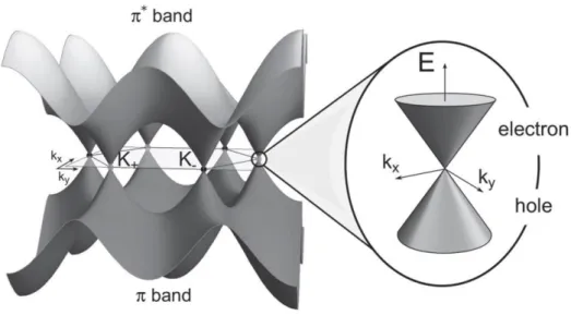
is fully occupied, while the (+) branch is empty, at least for electrically neutral graphene. Graphene displays a metallic (zero-gap) character. However, as the Fermi surface is of zero dimension (since it is reduced to a discrete and finite set of points), the term semi-metal or zero-gap semiconductor is usually employed (Torres, Roche et al. 2014).
Figure 3.3. Energy bands of graphene. The Dirac-like features are the linear energy dispersions, present near the neutral points K, K’. Taken from (Torres, Roche et al. 2014)
Expanding the equation above for k in the vicinity of K+(or K−), 𝐤 = 𝐊++ 𝛿𝐤(𝐤 = 𝐊−+ 𝛿𝐤), yields the linear dispersion5 ,for the π and π∗ bands near these six corners of
the 2D hexagonal BZ, 𝐸±(𝛿𝐤) =±ℏν𝐹|𝛿𝐤|, where ν𝐹 =√3𝛾0 𝑎 2ℏ = 3𝑡𝑎/2ℏ ≅ 106m/s
is the Fermi velocity (Obeng and Srinivasan 2011). This energy relation corresponds to massless relativistic particles in which the charge carriers have speeds 300 times less than the speed of light (Neto, Guinea et al. 2009, Sagar 2011). That is, charge carriers
19
travel through graphene as if they were massless Fermions obeying a Dirac equation (Wallace 1947, Obeng and Srinivasan 2011) (Castro, Novoselov et al. 2007).
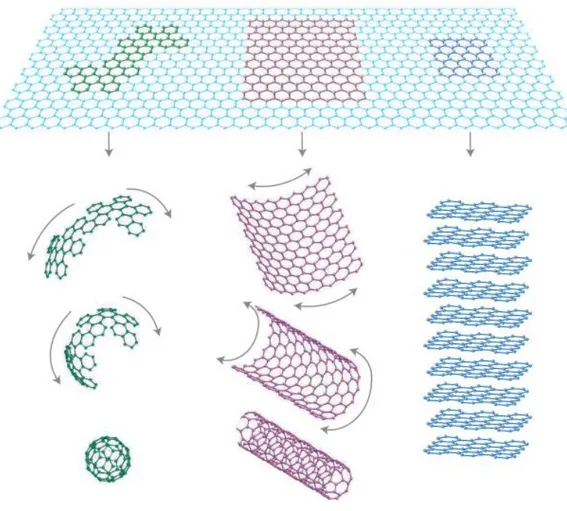
3.4. Carbon allotropes
Graphene has been envisioned as the building block of all other sp2-hybridized carbon allotrope forms (Figure 3.4) (Novoselov, Geim et al. 2004, Allen, Tung et al. 2009), including fullerenes, graphite, and GNRs (Wallace 1947). Interestingly though, graphene was the last allotrope to be (experimentally) discovered as it was presumed not to exist as a free standing material due to the unstable nature of 2D materials (Landau 1937, Obeng and Srinivasan 2011). Prior to 2004, graphene was known to exist only as a constituent part of graphite (Obeng and Srinivasan 2011, Torres, Roche et al. 2014). That year, however, scientists from Manchester University, Andrei Geim and Kostya Novoselev, isolated graphene for the first time and studied its ambipolar field-effect of their samples (Novoselov, Geim et al. 2004, Allen, Tung et al. 2009). This subsequently resulted in the popularisation of the material, especially amongst condensed-matter physicists and recently for the electron-device community (Deepak, Manoharan et al. 2011, Cao, Chen et al. 2012). Gem and Novoselev’s pioneering efforts were bagged with the Nobel Prize in Physics in 2010 (Dresselhaus and Araujo 2010, Hancock 2011). In the following sections it will be provided a brief review of each carbon allotrope.
Fullerenes are carbon molecules in which the atoms arrange in hollow shapes (sphere, ellipsoid, tube) (Hirsch 1994). The scientific community has focused research mainly in spherical fullerenes (also called buckminsterfullerene or buckyball) and cylindrical fullerenes (also called carbon nanotubes (CNTs) or buckytubes) (Hirsch 2009, Dumlich and Reich 2010). Buckyballs can be found in small quantities in soot, making them the most common fullerene found in nature (Lusk and Carr 2008). Fullerenes are similar in structure to graphite, but they may also contain pentagonal (or sometimes heptagonal) rings that make the planar structure to wrap.
20
Figure 3.4. The planar hexagonal structure of graphene can be considered as the building material for all other sp2-allotropes. i.e., it can be wrapped up into 0D buckyballs, rolled into 1D nanotubes or stacked into 3D graphite. Taken from (Geim and Novoselov 2007).
CNT exhibit a wide range of novel mechanical and electronic properties that could be applied in many fields, such as nanoelectronics, nanosensors, photonics, nanomechanical devices, among others (Jorio, Dresselhaus et al. 2007, Ismail, Ahmadi et al. 2012). However, the difficulty to synthesize them (Harris, Zhou et al. 2001, Liang 2008) and their incompatibility with planar technologies has led to the search of a successor material (Samadi and Faez 2013). GNRs fulfil those requirements, displaying similar electronic/magnetic properties to CNTs, being also compatibility with planar technologies (Chauhan and Guo 2010). This could solve large-scale integration hurdles of CNTs (Han, Özyilmaz et al. 2007, Samadi and Faez 2013).
3.5. Graphene nanoribbons
GNRs are basically elongated strips of single layered graphene with a finite width (typically less than 10 nm (Li, Wang et al. 2008, Wang, Ouyang et al. 2008)) that can
21
be obtained by cutting a graphene sheet along a certain crystallographic orientation (angle or chirality) (Barone, Hod et al. 2006, Dubois, Zanolli et al. 2009) (Figure 3.5). The microscopic structure of GNRs is closely related to that of graphene, and so their properties. However, due to the quantum confinement effect (QCE) (Torres, Roche et al. 2014) experienced by the electrons inside these quasi-one-dimensional (1D) structures, additional properties beyond that of graphene can be observed, e.g., opening of Eg (Han, Özyilmaz et al. 2007, Kan, Yang et al. 2011).
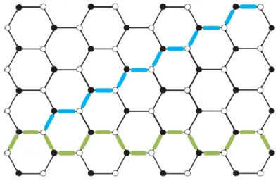
There are an infinite number of ways (chiralities) of cutting a sheet into a ribbon (Dutta and Pati 2010). Within the most studied GNRs are armchair (AGNRs) and zigzag (ZGNRs) edged nanoribbons, which show different charters: semiconducting and metallic, respectively (Han, Özyilmaz et al. 2007, Dutta and Pati 2010). Recent experimental studies reveal that ZGNRs possess localized edge states with energies near the EF (Nakada, Fujita et al. 1996, Kobayashi, Fukui et al. 2005). These edge states
correspond to the non-bonding molecular orbitals (Nakada, Fujita et al. 1996), and are responsible for the magnetism (Nakada, Fujita et al. 1996, Dutta and Pati 2010). Edge states are completely absent for AGNRs (Dutta and Pati 2010).
Figure 3.5. Honeycomb lattice of graphene with both zigzag (light blue) and the
armchair (green).
In addition to QCE and chirality, the electrical properties of GNRs are strongly dependent on their widths (w) and distortions at their edges. On the one hand, GNRs have shown to be semiconductors with band gaps that scale inversely against the nanoribbon width (Hancock, Uppstu et al. 2010). On the other hand, edge distortions
22
modify the edge states of the GNRs as their properties are associated primarily with the geometry rather than the chemistry itself (Chauhan, Srivastava et al. 2013).
Consequently, a deep understanding of the modification on the electronic structure and thermodynamic stability of GNRs is necessary before considering carbon allotropes as building blocks in silicon-based CMOS and related technologies (Dubois, Zanolli et al. 2009, Cao, Chen et al. 2012). In chapter 4, it is presented the results obtained from TB simulations of defected GNRs. The results put forward the way in which Eg can be
engineered (opened) through the insertion of defects at the edges of the GNRs.
3.6. Parametrization of the AGNRs into Atomistic Toolkit
Geometry optimization of AGNRs was carried out by DFT using a plane-wave basis set and PAW pseudopotentials for the description of the electron–ion interaction. Periodic boundary conditions perpendicular to the ribbon and the unit cell padding distance is set to 10 Å to reduce any residual electrostatic interactions with the periodic images of the ribbon. An energy cut-off value of 150 Ry was selected to ensure accurate results. The Brillouin zone k-point sampling was done by using the Monkhorst–Pack algorithm, and 1x1x100 k-points were chosen for the fully self-consistent calculations. The geometry for each AGNR studied was fully relaxed until the force on each of the atoms was less than 0.01 eV Å-1. To describe the electronic properties of the nanoribbon, it was found more suitable to use the TB approximation for the π electron as described in (Faez and Barami 2013, Uppstu 2014). A TB Hamiltonian (H) with modified hopping parameters was used to describe the band structure of the AGNRs. The one-orbital first-neighbor tight-binding model including the Hubbard term as follows: 𝐻 = ∑ 𝑡𝑖,𝑗𝑐𝑖,𝜎𝑡 𝑐 𝑗,𝜎+ 𝑈 ∑(𝑛𝑖,↑〈𝑛𝑖,↓〉 + 𝑛𝑖,↓〈𝑛𝑖,↑〉 𝑖 𝑖,𝑗 With 𝑐𝑖,𝜎𝑡 and 𝑐
𝑗,𝜎 being the creation and annihilation operators, respectively, for an
electron of spin 𝜎 in the π orbital of the ith carbon atom, and 𝑛𝑖,𝜎the corresponding
number operator. Here it was chosen t=-2.74 eV and U=-2t. The TB model is a very simple model for electronic structure calculations. Its advantage over ab initio methods is its low computational cost, which enables simulating systems that are large enough to
23
contain even millions of atoms (Uppstu 2014). Despite the simplicity of the model, it is relatively accurate, especially for carbon-based materials such as graphene.
In this work, atomic visualizations were done with Virtual NanoLab (VNL) (Toolkit) while calculations were done using the Atomix Toolkit (ATK) package (Toolkit , Simulator 2012).
Chapter 4.
Discussion of results
4.1. Introduction
The present research primarily was dedicated to study the electrical and structural properties of SnO2 and graphene materials from the theoretical viewpoint. Nonetheless,
experimental results, obtained through the collaboration with the Tyndall National Institute (Ireland) and the National Central University, Jhong-Li (Taiwan), were employed to booster the findings of the main line of investigation.
The DOS pattern and the band structure were used to predict the electrical behavior of the materials (e.g., type of conductivity and band gap width). The Bader population analysis along with a close examination of the spatial positions of the defect-nearby atoms shed light on their structural changes.
The resistivity, carrier mobility and the carrier concentrations of the TFT devices were conducted by Hall measurement. The crystalline parameters were investigated by XRD, while the dopant concentrations were examined by XPS. The carrier type and
25
carrier mobility of the GFET devices was carried out by field-effect measurements. The surface morphology was investigated in AFM. In addition, Raman spectroscopy was used to develop a qualitative analysis of the graphene flakes inside the FET structure.
4.2. Origin of the intrinsic n-type conductivity in SnO
2As already mentioned in Chapter 2 (section 2.4), the intrinsic ability of SnO2 to
conduct electrons has been often attributed to the presence of unintentionally created donor centers, usually identified as metallic interstitials or oxygen vacancies that produce shallow donor states near the CB edge (Varea 2007, Choi, Hwang et al. 2008). However, recently Singh et. al. (Singh, Janotti et al. 2008) have put forward an alternative scheme to explain this phenomena: the doping the SnO2 crystal with
interstitial/substitutional H atoms (Hi or Hsub). Both schemes were exploited as detailed
below.
4.2.1. First scheme to achieve n-type conductivity in SnO2
In the first scheme, the unintentional n-type conductivity observed in nominally pure SnO2 samples was reproduced by removing one of the host oxygen atoms (VO) located
in the central part of the supercell and by taking one tin atom from its lowest energy position to an interstitial one; this scheme will be called “the SnO2+VO+Sni scheme”
throughout this dissertation. The equilibrium configuration for this scheme is depicted in Figure 4.1 (the POSCAR file which contains the lattice geometry and the ionic positions of this configuration can be found in appendix A.1).
Only the atoms situated rather close to the point defect, up to 2.06 Å, tend to displace themselves in search for new stable positions (Table 4.1). The Coulomb electrostatic interaction is not the main source of the observed atomic movements with respect to the defect according to analysis of atomic charges obtained by the Bader population analysis implemented in the algorithm explained elsewhere (Henkelman, Arnaldsson et al. 2006). It is clear that atomic charges do not change notably except the charges on three Sn atoms situated close to the vacancy. Sn atoms which surround VO tend to
reduce their initial distances till the vacancy in order to fill the empty space left by the missing atom. Sn(1) and Sn(2) atoms displace by approximately the same amount while
26
Sn(3) atom shifts less since its charge suffers smaller change; additionally we suppose that Sn(3) might interact electrostatically with the Sni. So, the main reason of atomic
displacements could be the tendency to fill empty space created by the VO point defect.
Oxygen atoms rearrange themselves around Sn and Sni atoms in order to preserve initial
Sn–O bond lengths as close as those in the pristine structure of SnO2 (~2.05 Å).
Figure 4.1. Schematic diagram of the atomic displacements in SnO2 containing VO and Sni intrinsic point defects.
Total DOS, shown in Figure 4.2, was calculated in order to account for the changes of the compound’s electronic properties. The position of EF for the SnO2 containing the
VO+Sni pair is found at the bottom of the CB. That clearly indicates the existence of free
electron within the lower part the CB, which in turn ratifies the n-type electrical conductivity in the SnO2 crystal.
It is important to mention that VO alone does not show any trace of n-type
conductivity. Figure 4.3 shows the DOS pattern of a configuration in which only VO has
been included into the SnO2 lattice. The position of Fermi level, which lies in the
middle of the band gap, corroborates this fact. The POSCAR file which contains the lattice geometry and the ionic positions of this configuration can be found in Appendix A.2.
27
Table 4.1. Charges on atoms obtained by the Bader population analysis for the perfect (Q1) and n-type undoped (Q2) SnO2 crystals. The atomic displacements regarding the point-defect for atoms within the defective region are also shown. Negative atomics displacements stand for the defect-inward shifts. The atomic numeration corresponds to the one indicated in Figure 4.1.
Defect Q1 (e) Q2 (e) ΔR (Å) Nearby atoms
VO 2.41 2.01 -0.06 Sn (1) 2.41 2.04 -0.05 Sn (2) 2.42 2.12 -0.02 Sn (3) -1.20 -1.20 0.01 O (1) -1.21 -1.22 0.00 O (2) -1.21 -1.23 -0.02 O (3) -1.21 -1.21 0.02 O (4) -1.21 -1.22 0.01 O (5) -1.21 -1.23 -0.01 O (6) -1.21 -1.22 -0.03 O (7) -1.21 -1.21 -0.04 O (8) -1.21 -1.21 -0.04 O (9) -1.21 -1.22 -0.02 O (10) Sni -1.20 -1.20 -0.01 O (1) -1.21 -1.21 0.01 O (9) -1.21 -1.22 0.01 O (10) -1.21 -1.23 -0.01 O (11) -1.21 -1.22 0.00 O (12) -1.21 -1.23 0.00 O (13)
28
Figure 4.2. Total DOS of SnO2 endowed with n-type conductivity. The dashed grey line marks the EF.
Figure 4.3. Total DOS of SnO2 when VO has been added to the crystalline lattice. The Fermi level (dashed gray line) located in the middle of the band-gap suggest that no conductivity has been acquired by the crystal.
29
4.2.2. Second scheme to achieve n-type conductivity in SnO2
In the second scheme, the interplaying of Hi, Hsub and/or VO point defects within
lattice sparked the alluded n-type conductivity in SnO2. Data in this section, obtained
from nine configurations, has been organized into three main categories (Table 4.2) and detailed below.
Figure 4.4. Schematic diagram showing considered positions for the VO and H atom in the pure SnO2 lattice.
The first group (SnO2+VO+H in Table 4.2) describes the cases in which the H atoms
were placed inside an oxygen deficient SnO2 lattice (VO included). The locations that
the H atoms assumed with respect to VO were P1 (7.1 Å from VO), P2 (6.3 Å from VO)
and P3 (5.0 Å from VO) in Figure 4.4. The fourth configuration in SnO2+VO+H
represents the case in which the H atom was situated at the VO site, therefore being
considered as a substitutional H atom. In the second group (SnO2+H in Table 4.2) the H
atom was placed at P1, P2 and P3 in Figure 4.4. In contrast to the SnO2+Vo+H group, VO
was not included within the lattice in this group. Modelling of the second group of configurations was carried out in order to determine the contribution of VO to the n-type
conductivity of SnO2 (if any). Finally, the third group (SnO2+2H in Table 4.2) describes
30
were performed in order to determine development of the n-type conductivity as the concentration of H was increased.
Analysis of the total energies of the configurations in SnO2+Vo+H indicates that P1,
P2, and P3 sites were equally favorable. Hsub site was found to be the most stable
configuration, displaying a total energy of roughly 0.8 eV lower than that of the other sites. This is in perfect agreement with the work of Singh et. al.(Singh, Janotti et al. 2008).
By comparing the DOS patters of the first two groups (Figure 4.5 and Figure 4.7), one can notice that in the presence of VO there exist a local occupied state situated about
0.98 eV above the upper VB edge. This state can be interpreted as a localized F-center in SnO2 due to the VO. Formation of F-center as well as practically equal free-carrier
densities with and without VO (Table 4.2) implies that presence of VO is not required at
all for SnO2 in order to exhibit n-type electrical conductivity.
Values of free-carrier density, n, calculated in electrons per cubic centimeter (cm3) for the configurations investigated in this section were in good agreement with the available experimental findings (Goyal, Agashe et al. 1993, Kılıç and Zunger 2002) for nominally undoped SnO2 crystals. n was calculated by integrating the product of the
density of states (𝑔𝐶(𝐸)) with the probability density function (𝑓(𝐸)) from the bottom
of the CB (labelled 𝐸𝐶) up to the Fermi level (EF) in the corresponding DOS patterns
and is expressed as follows:
𝑛 = ∫ 𝑔𝐸𝐸𝐹𝐶 𝐶(𝐸)𝑓(𝐸)𝑑𝐸 4.1
For a deeper description of the method look through reference (Hu 2010).
No big difference could be appreciated between n of the configurations of the first group. Also, n for the first group is similar to those of the SnO2+H group. These
preliminary results lead to the conclusion that VO does not contribute to the generation
31
Table 4.2. Free-carrier density (n), O-H bond length, and atomic charges on H are summarized for each one of the configurations depicted in Figure 4.5. The
POSCAR file which contains the lattice geometry and the ionic positions of the best configuration can found in Appendix A.3.
Group Positions of H n (e / supercell) n (e / cm3) O-H bond (Å) QH (e)
SnO2+Vo+H P1 1.002 8.772*1020 0.998 0.63 P2 1.006 8.825*1020 0.999 0.62 P3 0.969 8.485*1020 0.999 0.62 Vo 1.010 8.877*1020 -0.48 SnO2+H P1 1.022 8.995*1020 1.001 0.61 P2 1.021 8.950*1020 1.000 0.62 P3 1.010 8.846*1020 1.000 0.62
SnO2+2H P1 & V0 2.042 1.778*1021 1.002 0.64 & -0.47
32
Figure 4.5. DFT+U computed total and partial DOS for SnO2+VO+H configuration if the H atom is at the site P1. The dashed gray line marks the EF. Integration from the bottom of the CB up to EF represents the value of free-carrier density: n. DOS patterns for the rest of the group SnO2+VO+H configurations are practically identical.
Addition of H atom and VO into the SnO2 crystalline lattice produced perturbation
and consecutive shifts for the atoms situated close to the point defects. As one can observe from Figure 4.6, the atomic displacements are predominantly inward with respect to the H impurity for oxygens and mainly outward for Sn atoms. The O-H inter-atomic distance was found to be ~1.0 Å. Computed inter-atomic charges, using the Bader population analysis show, small increase, about 0.03 e on average per atom, when H has been introduced thus implying importance of Coulomb electrostatic interaction in lattice distortion. Positive atomic charges on H (Table 4.2) demonstrate that it loses its only electron after being inserted into the material. Apparently, this electron becomes a free carrier. Negative charge on hydrogen in case of the VO configuration can be explained
33
(a) (b)
Figure 4.6. Atomic displacements in SnO2 crystal if hydrogen atom is situated at (a) the P1 site and (b) within the oxygen vacancy. The thickness of the arrows give an idea of the magnitude of the displacements. White, red and blue spheres stand for hydrogen, oxygen and tin atoms, respectively.
Figure 4.7. DFT+U computed total and partial DOS for SnO2+H configuration if the H atom
is at the site P1. The grey dashed line marks the EF. Integration from the bottom of the CB up to EF represents the value of free-carrier density: n. DOS patterns for the rest of the group SnO2+H configurations are practically identical.
34
4.3. Transition of the conductivity in SnO
2from n-type to p-type
The p-type electrical conductivity in the SnO2 was reproduced by codoping6 the
n-doped crystal (from section 4.2.1) with low concentrations of Al and N atoms. The cooping has been achieved by replacing one host O atom by the N impurity and four Sn atoms by four Al impurities, respectively. The computational values for the dopant concentrations, shown in Table 4.3, were kept as close as possible to the corresponding experimental values (X-ray diffraction (XRD) and X-ray photoelectron spectrometer (XPS) measurements detailed below).
Table 4.3. Impurity doping rates used in the computational and experimental procedures.
Dopant Theoretical (mol%) Experiment (mol%)
N 1.56 1.94
Al 12.48 14.65
Six different defect configurations have been considered by taking into account various relative positions between the intrinsic defects and dopants. The most stable configuration is shown in Figure 4.8; its POSCAR files can be found in Appendix A.4.
From a microscopic standpoint it can be observed that the incorporation of Al and N atoms into the crystallographic lattice produces a perturbation on the defect-neighbouring atoms situated within a radius of up to 2.96 Å from the corresponding point defect. Bader population analysis (Table 4.4) shows that the charges on Al atoms (Q1) are bigger than those of the Sn atoms (Q0), which are replaced in the process of
codoping. The charges for O atoms (Table 4.5) before and after codoping differ as well. It is possible to notice that oxygens in vicinity of impurity atoms become more negative. That is why we suggest the augmentation of ionic character in the chemical bonding within the defective region and Coulomb electrostatic origin for the atomic movements, especially between the Al and O atoms. Similar results regarding the atomic shifts have been recently obtained also for the Ga-doped SnO2 (Stashans, Puchaicela et al. 2014).In
case of N impurity (Table 4.5), atomic charge on nitrogen is smaller compared to the charge of the replaced O atom before codoping. This apparently leads to a smaller