Bottle-brush-shaped heterostructures of NiO-ZnO nanowires:
growth study and sensing properties
C. Baratto1,2, R. Kumar1,2,5, E. Comini1,2, M. Ferroni2,3, M. Campanini 4 1SENSOR Lab, CNR-INO Via Branze 45, Brescia Italy
2SENSOR Lab, Brescia University, Dept. of Information Eng., Via Branze 38, Brescia, Italy
3CNR-IMM Sezione di Bologna, via Gobetti 101 - 40129 Bologna,Italy 4EMPA, Überlandstrasse 129, 8600 Dübendorf (Zürich)
5Present address: University of Oslo, Department of Physics/Center for Materials Science and Nanotechnology (SMN), P.O. Box 1048, Blindern, NO-0316 Oslo, Norway
corresponding author: [email protected]
Abstract
We present here heterostructured ZnO-NiO nanowires, constituted by a core of single crystalline ZnO nanowires, covered by poly-crystalline NiO nanorods. The bottle-brush shape was investigated by SEM and TEM, confirming that a columnar growth of NiO occurred over the ZnO core, with a preferred orientation of NiO over ZnO nanowires. The heterostructured devices are proposed for gas sensing application. Bare ZnO nanowires and heterostructured sensors with two different thicknesses of NiO poly-crystalline nanorods were analysed for acetone, ethanol, NO2 and H2 detection. All sensors maintained n-type sensing mechanism,
with improved sensing performance for lower thickness of NiO, due to high catalytic activity of NiO. The sensing dynamic is also strongly modified by the presence of heterojunction of NiO/ZnO, with a reduction of response and recovery times towards ethanol and acetone at 400°C.
Keywords
Heterostructure; chemical gas sensor; TEM; nanowires; ZnO; NiO
1. Introduction
During the last decade, nanosized heterostructures of ionic metal oxides have attracted much attention because they possess improved physico-chemical properties with respect to their single-component counterpart. They are employed in light-emitting devices [1], ultraviolet sensors [2], photocatalyst [3], and gas sensors [4], [5]. Stimulated by these interesting applications, various techniques have been developed to realize heterojunction in one-dimensional (1D) nanostructures of metal oxides [2, 4, 6,
7].
Metal oxide gas sensors are used as low cost device for detection of pollutant gases [8-10], based on the change in electrical resistance upon interaction with gas species at elevated temperatures (300-500°C). The gas sensing performance is primarily influenced by the morphology, dimension, specific surface area, grain size, pore size of inter- and intra- materials, and agglomeration of the active material. In 2001, the use of 1D single crystalline nanowires (NWs) has been introduced to take advantage of the high sensor stability coupled to high surface to volume ratio [11].
Among 1D sensors, heterostructuring may be used to enhance sensitivity or selectivity of the device. 1D NWs can be either decorated with noble metal nanoparticles, that act as a catalyser towards the gas of interest [12] or layered with another metal oxide, which acts itself a catalyst [13], [14]. If the host semiconductor is n-type and the catalyst one is p-type or viceversa, one could take advantage of n-p heterojunction at the interface between the two materials. The superior functional performances of these systems in comparison to the corresponding single-phase metal oxide are mainly ascribed to the build-up of an inner electric field at the interface of the n-p junction [15] and to the catalyst action
of the decorating material [14]. The idea to combine different physical and sensing properties of individual components has been exploited in different configurations: ZnO-SnO2 [16], Cu2O-ZnO[4], Co3O4/ZnO, Cr2O/ZnO, In2O3/NiO[5], Fe2O3/ZnO [17].
Heterostructured NiO-ZnO couple is interesting for gas sensing application: NiO shows good catalytic properties [18], even if being a p-type, its response is lower with respect to the one of n-type metal oxide semiconductor [20]
NiO can be used as a core material with outer “shell”of ZnO [21, 22], or it can be used as the outer material to promote the kinetic of response to gases as done in thick film gas sensors [23, 24]. ZnO-NiO combination was investigated by Liu et al., who synthesized flowers-like structures of tapered wires of ZnO covered by round particles of NiO [14] and by Na et al., who decorated ZnO NWs by particles of NiO [25].
Here we would like to exploit the highly interconnected shape of ZnO single crystalline NWs bundles, together with the columnar growth of NiO nanorods (NRs). The promising characteristic of the heterostructured device was observed in a preliminary investigation [26]. In the current work we demonstrate that the sputtering deposition of NiO over ZnO NWs in special conditions give rise to a columnar growth of polycrystalline NRs with preferential orientation determined by material matching at the interface. This ensures a highly porous structure that interacts with gases mainly with the NiO surface, while the electrical signal is driven mainly through the ZnO single crystalline structure. A detailed morphological and structural investigation is presented, together with preliminary gas sensing analysis and a functional model for sensing.
2. Methods
2.1. Sensing device preparation
ZnO NWs were obtained by vapour phase growth from ZnO powder; Au catalyzer was preliminary deposited by RF sputtering on 2×2 alumina substrate before NWs growth to obtain dense distribution of NWs. The gold catalyst was deposited by RF magnetron sputtering at a pressure of 5 mbar, and for 1s with a power of 75W.
Growth was carried out in an evacuated tubular furnace, where Ar, the carrier gas, was controlled by mass flow meters up to 100 sccm. Zinc oxide powder was preferred as source material, compared to zinc, to restrain the evaporation rate. The oxide powder was placed on an alumina crucible at a temperature of 1370°C at 100 mbar to induce its evaporation. The substrates, catalysed with gold nanoparticles, were placed at lower temperatures, approximately 570°C. The 100sccm argon flow was kept constantly during all the deposition process.
Nickel oxide was deposited over ZnO NWs mesh by RF magnetron sputtering, starting from a nickel oxide target (99.99% pure, 4” size from CERAC). The parameters used during depositions were: room temperature, gas pressure 10-2 mbar (50%Ar/50%O
2), power 100W. In order to investigate the influence of NiO thickness over sensing properties, we used two different deposition times, one double of the other, that resulted into a NiO layer of 20 nm and 40 nm respectively (as observed at the electron microscope). The resulting heterostructured samples will be named hereinafter Ni-Zn-O-short for the lower NiO thickness and Ni-Zn-O-long for the higher NiO thickness. Uncoated ZnO NWs sensors were prepared as well for comparison.
2.2. Characterization by electron microscopy
Surface morphology was investigated by Scanning Electron Microscopy (SEM), operated in the 5-10 keV beam energy range. Samples, in their pristine state, were observed in the secondary-electrons imaging mode.
For observation and microstructural characterization in the Transmission Electron Microscope (TEM), samples were gently scratched with a knife blade over a holey-carbon film TEM grid. Owing to the small dimension of the fabricated heterostructure, the NWs are readily transparent to the energetic 200-keV electron beam of the TEM, allowing immediate conventional characterization through
bright-field imaging and electron diffraction analysis. TEM investigation was carried out by means of a JEOL JEM ARM 200F. The microscope was operated at 200 kV in TEM mode.
2.3. Functional tests with gases
For functional tests Pt electrodes and heater were deposited by RF magnetron sputtering. A Pt meander was deposited on the back side of the substrate to provide heating. The sensing layers were aged on the TO-5 case by heating the sensors at 500 °C in ambient air for two weeks prior to measurements.
Sensing tests were performed in a stainless steel test chamber (1 litre) at an ambient temperature of 20 °C atmospheric pressure, using a constant flux (300 cm3/min) with 50% relative humidity (RH). A constant bias (1 V direct-current) was applied to the sensing film and the electrical current was measured by a picoammeter (Keithley model 486). The system used to dynamically reproduce environmental conditions in a controlled and repeatable way is based on volumetric mixing through mass flow controllers and certified bottles.
We tested reducing gases (ethanol, acetone and hydrogen) and oxidizing gas (NO2). All gases were diluted in humid synthetic air. Sensor were tested at constant temperature of 300°C - 400°C - 500°C. Relative response towards reducing gases was calculated as sensor Response = R = (IF-I0)/I0, where IF is the steady state value in gas and I0 is the steady state in air. Relative response towards oxidizing gases was calculated R = (I0-IF)/I0, where IF is the steady state value in gas and I0 is the steady state in air. Response (Recovery) times were calculated as the time needed to reach 90% (70%) steady state value in gas (air).
3. Results
3.1. SEM and TEM characterization
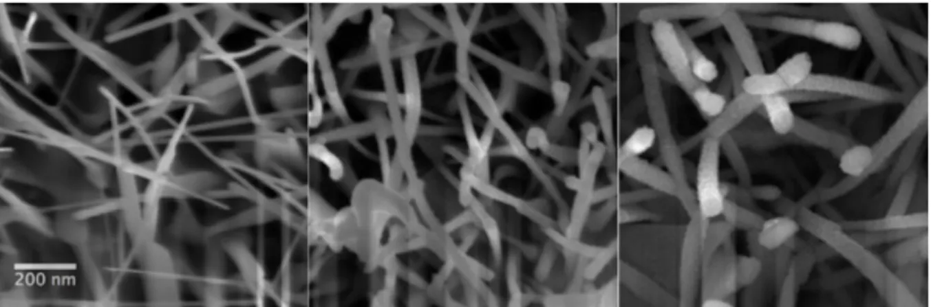
SEM was used to characterize the morphology of the sensing layers and to present the fabrication of the heterostructure. Figure 1-left shows the Zn-O nanostructure: thin NWs with diameter ranging between 20-30 nm cover the substrate with no evidence of an aligned arrangement. Figure 1-center demonstrates that after deposition of a thin coverage of Ni-O (sample Ni-Zn-O-short) the NWs are quite homogeneously covered and accordingly the diameter of the wires increased to about 40-60 nm. A further increase of the duration of the Ni-O deposition leads to a granular and thicker coverage for the Zn-O NWs, which is clearly visible in Figure 1-right (sample Ni-Zn-O-long).
Figure 1: (Left) secondary-electrons morphological image of the Zn-O NWs; (Center) coverage of the Zn-O NWs by the Ni-O sputtered layer in the Ni-Zn-O-short sample; (Right) increase of the heterostructure width and visible granularity for the Ni-O outer shell in the Ni-Zn-O-long sample.
TEM investigation reveals the microstructural assembling of the heterostructure. Figure 2 shows the bright field images of the ZnO-NWs covered by the NiO-shell. For the two samples, the granularity of the coverage previously observed is here highlighted as a polycrystalline structure that uniformly generates from an underlying backbone. Even if the average width of the structures agrees with the SEM observations, the position of the Zn-O nanowire does not always appear in the middle of the heterostructure. This is a direct evidence that the sputtering process does not results in a uniform
thickness for the Ni-O, as the random orientation of the Zn-O NWs unbalances the accumulation of Ni-O.
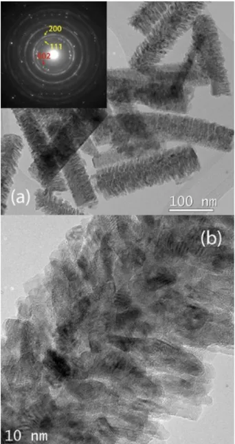
Figure 2-(a) and the relative inset presents the Ni-Zn-O-short sample: because of the TEM specimen preparation, small fragments of the long nanostructure are visible. At this scale, the samples are morphologically homogenous and feature a polycrystalline coverage nucleating from the underlying Zn-O nanowire. Taking into account the NiO shell, the diameter of the wires ranges 40-65 nm. The uniformity in contrast and the parallelism in the texture of the outer shell suggests some degree of ordered attachment of the Ni-O grains to the Zn-O nanowire. The selected area diffraction pattern, obtained from a region containing one nanowire and shown in inset of Figure 2 (a), presents a number of diffraction rings corresponding to the cubic phase of NiO, together with some intense reflections from the hexagonal crystalline phase for ZnO, according to the expected single-crystalline structure for the ZnO nanowire. Such a diffraction pattern corroborates the description of the heterostructure, as the polycrystalline nature of the NiO wires give rise to a typical powder-like diffraction pattern (with many concentric rings) superimposed to the diffraction spots owing to the oriented ZnO cores.
When the electron diffraction pattern is acquired over a very limited area of the structure, the intensity of the diffraction rings pertaining to NiO increases in correspondence of the ZnO diffraction spots, indicating that the texturing for the shell is promoted by a lattice match between the 111-NiO and the 200-ZnO reflections.
Figure 2 (b) shows the morphology of the polycrystalline NiO at higher magnification. Lattice fringes are visible in the high-resolution TEM picture, indicating the the NiO outer shell is formed by crystalline grains with diameter less than 10 nm.
The ZnO nanowire, backbone of the longitudinal
nanostructure, measures about 20 nm in width
.
Figure 2: (a) TEM bright field image and the relative electron diffraction pattern (inset) of the Ni-Zn-O-short
sample. The morphology and diffraction indicates a textured cubic NiO (Yellow arrow)- hexagonal ZnO (Red arrow) heterostructures for the specimen. (b) Detail of the ZnO-NiO heterostructure at high magnification, showing the crystalline grains of the NiO coverage of the ZnO NW.
Figure 3: TEM bright field image and detail at higher magnification (inset) of the textured cubic NiO -
hexagonal ZnO heterostructures for the the Ni-Zn-O-long sample. The sample features and increased width, and the inset highlights the uneven accumulation of NiO.
Figure 3 shows the increase in width to 90-110 nm for the Ni-Zn-O-long sample as a result of the prolonged deposition, with no significant morphological changes for the heterostructure. The crystalline phases are confirmed. The inset shows that the thickness of the NiO outer shell is not even with respect to the longitudinal ZnO NW, such asymmetry is ascribed to the sputtering process of deposition of the Ni-O.
3.2. Electrical characterization
The electrical characterization of ZnO Nws and Ni-Zn-O devices was carried out in air and in selected gas species.
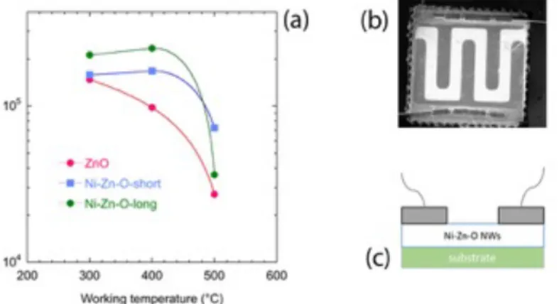
Figure 4 (a) reports about the baseline resistance (Rair) of the sensors tested in synthetic air with 50% R.H. at 20°C. The device temperature was controlled using the backside Pt meander. Figure 4 (b) is the low magnification SEM image of the sensing device: Pt interdigitated contacts were deposited over the sensing layer, which is the brighter area. As depicted in the scheme in Figure 4 (c), the contacts are deposited on top of the NWs structure.
The Rair of Ni-Zn-O sensors (both samples) at 300°C is slightly higher than the one of ZnO sensors, but it is not so different. Resistance decreased with temperature for ZnO NWs as expected. Resistance of Ni-Zn-O sensors also decreased with temperature, when temperature was modified from 400 to 500°C.
A schematical model of the ZnO and NiO heterostructure can be considered as the parallel of two resistors RZnO and RNiO. If the RNiO is much higher than RZnO then the resulting RNi-Zn-O would be similar to RZnO as observed. Thus we can figure out that the current mainly flows into ZnO NWs backbone, and the contribution of NiO NRs is considered through the p-n junction.
Figure 4: (a) Baseline resistance values in humid air (50% relative humidity) at different working temperatures; (b) SEM image at low magnification showing the alumina substrate with sensing layer (brighter areas) and IDC contacts (darker areas) and welding gold wires; (c) cross-sectional scheme of sensing device, showing the IDC contacts on top of sensing Ni-Zn-O NWs.
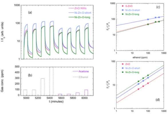
Figure 5 (a-d) shows the dynamic response towards ethanol and acetone at 400°C. ZnO NWs device behaves as n-type semiconductor, as expected. NiO/ZnO heterostuctures showed n-type behaviour as well, independently from NiO amount. Since NiO layer deposited by sputtering behave as p-type gas sensor [19], while ZnO is typically n-type, this is again in agreement with the hypothesis that the current flows mainly into the n-type ZnO NWs, while the interface with gas is with NiO.
From the point of view of the sensing properties we can remark two main effects of the use of the Ni-Zn-O: the first one is the sensor response increase, while the second one is the lowering of response and recovery times during ethanol and acetone detection.
The sensor response increase was observed for both ethanol and acetone at 400°C for Ni-Zn-O-short sample - Figure 5 (b) – with respect to ZnO Nws and Ni-Zn-O-long sample - Figure 5 (a) and (c). Figure 5 (e-f) shows the relative response towards gas concentration (calibration curves). Experimental data were fitted using a power law:
R= A*[C(ppm)]B
where C is the concentration in ppm and R = (IF-I0)/I0 is the sensor response.
By extrapolating the fit of the heterostructured sensors to the axis limit, a detection limit of 1 ppm is reached by the Ni-Zn-O-shortsensor.
For ethanol detection – Figure 5 (e) - saturation behaviour is observed for ZnO NWs; the fit line has been reported as guide for the eye, but the extrapolation to the axis limit is not reliable. Instead, no saturation was observed for Ni-Zn-O-longand Ni-Zn-O-short.
These data shows that only for the optimal thickness used in Ni-Zn-O-short sensor response is increased, while there is no gain with longer NiO NRs as in Ni-Zn-O-long.
At 400°C, both the heterostructured sensors in Figure 5 (b) and (c) have faster dynamic in absorption and desorption of acetone and ethanol with respect to pristine ZnO NWs – Figure 5 (a).
To study the dynamic of sensors, response and recovery times (Tres, Trec) were calculated. To show the reduction of response and recovery times obtained using Zn-Ni-O sensors at 400°C, we plotted in Figure 6 the “Rational Response Time”=Tres[Ni-Zn-O]/Tres[ZnO] and “Rational Recovery Time”=Trec[Ni-Zn-O]/Trec[ZnO]. A major improvement can be observed in either response times and recovery times to ethanol and acetone, since the numbers obtained are always lower than 1. The reduction is to 60-50% of the initial value for Tres and to 30% or more for Trec.
Sensor Ni-Zn-O long is the most effective in reducing response and recovery times that are around 1500 s for the response time and 210 s for the recovery time.
Figure 5: Dynamic response (I/I0) at 400°C for (a) ZnO NWs, (b) Ni-Zn-O-short, (c)Ni-Zn-O-long; (d) Plot of
gas pulses for the measurements (a-c): (e) Calibration data towards acetone (25-50-100ppm) for sensors working at 400°C; (f) Calibration data towards ethanol (100-300-500 ppm) for sensors working at 400°C;
Figure 6: (a) Rational Response Time and Rational Recovery Time of Ni-Zn-O sensors referred to the response
and recovery times of ZnO. Values considered are 100 ppm of ethanol and 50 ppm of acetone. The reduction of response and recovery times at 400°C can be observed since the value is always lower than unity.
At 500°C the sensors behaviour towards ethanol and acetone is different (Figure 7). Sensing response is increased ten times for all sensors with respect to 400°C. The higher response is still observed for Ni-Zn-O-shortsensor. This is clearly seen in the dynamic plot (Figure 7 (a)) and is resumed in the calibration plot (Figure 7 (c)). At so high working temperature, no reduction of response and recovery times is obtained using Ni-Zn-O sensors with respect to ZnO NWs: the dynamic data of the three sensor have been plotted normalizing them at the baseline current to show the similarity in response
and recovery times. In order to reduce power consumption of gas sensors, the lowest possible operating temperature should be used (400°C).
Figure 7: (a) Dynamic response (I/I0) at 500°C for ZnO NWs, Ni-Zn-O-short, andNi-Zn-O-long , normalized to
the baseline values; (b) Plot of gas pulses for the measurements in (a); (c) Calibration data towards ethanol (100-300-500 ppm) for sensors working at 500°C.; (d) Calibration data towards acetone (25-50-100ppm) for sensors working at 500°C.
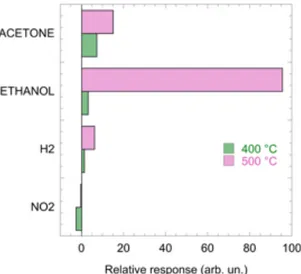
The cross – sensitivity towards other gases (H2 and NO2 ) in the temperature range 300°C-500°C was investigated. At 300°C the response to reducing gases is poor both in term of dynamic and relative response, while response to NO2 is observable (see supporting information S2). The cross sensitivity plot of sensor Ni-Zn-O-short at 400°C and 500°C is shown in
Figure 8
for the sample Ni-Zn-O-short. Relative response to NO2 is shown as a negative value to take into account that it is an oxidizing species. At 400°C, poor response to 500 ppm of hydrogen is recorded, while high response to acetone is observed.At 500°C,
a significant response towards ethanol with respect to the other gases was observed.
The presence of NiO NRs shell (for the Ni-Zn-O-short sensor) further enhances the ethanol
detection already observed in this study for ZnO NWs (see supporting information S1) and in
literature for ZnO and ZnO/NiO sensors working at high temperatures [27, 25].
The low response to NO
2at 400 and 500°C is in line with different optimum working
temperature for ZnO based material for detection of reducing and oxidizing gases [a, c,e –
inserire referenze].
By comparing the results obtained with literature [21,22] we can affirm that the use of NiO nanorods as external shell over ZnO nanowires produced an increase in sensor response to ethanol, with respect to results obtained with ZnO outer shell over NiO core.
Figure 8: Relative response of sensor Zn-Ni-O-short to NO2 (5ppm), H2(500 ppm), Ethanol (100 ppm) and Acetone (50 ppm) in humid air. Sensor was operated at 400°C and 500°C.
4. Discussion
In the hybrid structure considered here, NiO NRs densely covers the ZnO NWs, but is feasible that the Pt IDC is in contact with both ZnO and NiO. Thus, the current would flow in parallel through ZnO NWs and NiO NRs, but, as discussed in the comments to the Fig 4, the main contribution comes from ZnO NWs. Moreover the sensor signal is n-type, indicating again that the conduction should take place mainly in the n-ZnO.
Since ZnO NWs are covered by NiO NRs, we hypothesize that the interaction of gas species occurs mostly on the surface of NiO. Between NiO NRs and ZnO NW a p-n heterojunction is formed and this influences the sensor behaviour.
For a semiconducting gas sensor, the reducing gas (ethanol) reacts with the oxygen adsorbed over the surface [28],
𝐶"𝐻$𝑂𝐻 + 𝑂"' → 𝐻"𝑂 + 𝐶𝑂"+ 𝑒* (1) releasing an electron into the conduction band of the metal oxide.
Figure 9 (a) shows the mechanism for ZnO NWs: the depletion region at the surface of the NWs is reduced after gas interaction, thus an increase in current flowing through the NWs is observed - Figure9(c).
In heterostructured Ni-Zn-O - Figure 9 (b) - the interaction occurs with the surface of NiO. During stabilization in air, the NiO particle is in accumulation state, since O2- adsorbed on the surface attracts holes that are majority carriers in NiO. After interaction with reducing gases, an electron is released back and recombines with holes: the amount of negatively-charged-oxygen on the surface of NiO is reduced.
At the interface of ZnO/NiO a reverse biased p-n junction is present both in air and in gas. In presence of reducing gas, the negative charge is diminished, thus the bias polarizing the junction is reduced; as a result, higher current can flow in the ZnO NWs for Ni-Zn-O sensors - Figure 9 (d).
The observed increase in sensor response for Ni-Zn-O-short, is ascribable to increased oxygen ionosorption reported for NiO with respect to ZnO [14]; thus more ionosorbed oxygen would be available to interact with reducing gases by the reaction (1).
For highest thickness of NiO (Ni-Zn-O-long), the decrease in relative response with respect to ZnO could be ascribed to the competing p and n contributions from NiO and ZnO, since a reduction of the current is expected for p-type material, while increase is expected for n-type. The same competing contribution could be also present in the case of Ni-Zn-O-short, but the balance between the two materials would be more favourable in this case.
Another effect observed in our experiments is the strong decrease in response and recovery times at 400°C. This has been already reported in literature for other metal oxides loaded with NiO, ascribing this to a catalytic surface reaction assisted by NiO [23, 24]. When the sensor is working at 500°C, the dynamic of ZnO NWs is sufficiently fast and the difference between ZnO NWs and ZnO/NiO becomes negligible.
Figure 9: Scheme of the gas sensing mechanism for (a)-(c) NiO NWs and (b)-(d) ZnO/NiO heterojunction for
interaction with ethanol.
Conclusions
The current work demonstrates that ZnO single crystalline NWs bundles can be heterostructured with NiO NRs with preferred orientation.
SEM and TEM investigations showed a bottle-brush shape confirming that a columnar growth of NiO NRs occurred around the single crystalline ZnO nanowire core. The deposition of NiO by sputtering for a longer time induced a longer NRs growth, but the preferred angle of growth of NiO over ZnO is maintained, indicating a preferred growth mechanism.
The p-n heterojunctions were tested for gas sensing and their properties were compared to th ones of bare ZnO NWs
Ni-Zn-O sensors showed n-type sensing behaviour. Ni-Zn-O-short has an increased sensor response towards ethanol and acetone for 400°C and 500°C working temperature.
A major improvement can be observed in response times at 400°C, for both thickness of NiO. The reduction is to 60-50% of the initial value for Tres and to 30% or more for Trec. Decreased response and recovery times are due to catalytic surface reaction assisted by NiO, in agreement to what reported in literature for other oxides.
The cross – sensitivity towards other gases (H2 and NO2) was checked, indicating a preferential response to acetone at 400°C, and to ethanol at 500°C.
A model for sensing mechanism has been presented and discussed, taking into account the n-type behaviour of sensing devices, and the p-n junction at the interface between ZnO NWs and NiO NRs. Acknowledgements
The research leading to these results were partially funded by the NATO Science for Peace and Security Programme under grant N° 9085043. The TEM measurements were performed at INFIM Institute in Bucharest (Dr. C. Ghica and Dr. R. Damian) and supported by CERIC Consortium (proposal 20152072).
References
[1] Park W I and Yi G C 2004 Electroluminescence in n-ZnO Nanorod Arrays Vertically Grown on p-GaN Advanced Materials 16 87-90
[2] Li Y-R, Wan C-Y, Chang C-T, Tsai W-L, Huang Y-C, Wang K-Y, Yang P-Y and Cheng H-C 2015 Thickness effect of NiO on the performance of ultraviolet sensors with p-NiO/n-ZnO nanowire heterojunction structure Vacuum 118 48-54
[3] Chang S-H, Yang P-Y, Lai C-M, Lu S-C, Li G-A, Chang W-C and Tuan H-Y 2016 Synthesis of Cu/ZnO core/shell nanocomposites and their use as efficient photocatalysts CrystEngComm 18 616-21
[4] Li J, Li H, Xue Y, Fang H and Wang W 2014 Facile electrodeposition of environment-friendly Cu2O/ZnO heterojunction for robust photoelectrochemical biosensing Sensors and Actuators B: Chemical 191 619-24
[5] Kim H J, Jeong H M, Kim T H, Chung J H, Kang Y C and Lee J H 2014 Enhanced ethanol sensing characteristics of In2O3-decorated NiO hollow nanostructures via modulation of hole accumulation layers ACS Appl Mater Interfaces 6 18197-204
[6] Lee Y-M, Yang H-W and Huang C-M 2012 Effect of rapid thermal annealing on the structural and electrical properties of solid ZnO/NiO heterojunctions prepared by a chemical solution process Journal of Physics D: Applied Physics 45 225302
[7] Qu Z, Fu Y, Yu B, Deng P, Xing L and Xue X 2016 High and fast H2S response of NiO/ZnO nanowire nanogenerator as a self-powered gas sensor Sensors and Actuators B: Chemical 222 78-86 [8] Epifani M, Diaz R, Arbiol J, Comini E, Sergent N, Pagnier T, Siciliano P, Faglia G and Morante J 2007 Oxide nanocrystals from a low-temperature, self-limiting sol–gel transition in a coordinating environment: Nanocrystal synthesis, processing of gas-sensing devices and application to organic compounds Sensors and Actuators B: Chemical 126 163-7
[9] Mirzaei A, Leonardi S G and Neri G 2016 Detection of hazardous volatile organic compounds (VOCs) by metal oxide nanostructures-based gas sensors: A review Ceramics International 42 15119-41
[10] Comini E, Baratto C, Concina I, Faglia G, Falasconi M, Ferroni M, Galstyan V, Gobbi E, Ponzoni A, Vomiero A, Zappa D, Sberveglieri V and Sberveglieri G 2013 Metal oxide nanoscience and nanotechnology for chemical sensors Sensors and Actuators B-Chemical 179 3-20
[11] Comini E, Faglia G, Sberveglieri G, Pan Z and Wang Z L 2002 Stable and highly sensitive gas sensors based on semiconducting oxide nanobelts Applied Physics Letters 81 1869
[12] Zampiceni E, Faglia G, Sberveglieri G, Kaciulis S, Pandolfi L and Scavia G 2002 Thermal Treatment Stabilization Processes in SnO2 Thin Films Catalyzed With Au and Pt Ieee Sens J 2 102-6 [13] Lee J S, Kwon O S, Park S J, Park E Y, You S A, Yoon H and Jang J 2011 Fabrication of Ultrafine Metal-Oxide-Decorated Carbon Nanofibers for DMMP Sensor Application Acs Nano 5 7992-8001
[14] Liu Y, Li G, Mi R, Deng C and Gao P 2014 An environment-benign method for the synthesis of p-NiO/n-ZnO heterostructure with excellent performance for gas sensing and photocatalysis Sensors and Actuators B: Chemical 191 537-44
[15] Liang Y-C, Hsia H-Y, Cheng Y-R, Lee C-M, Liu S-L, Lin T-Y and Chung C-C 2015 Crystalline quality-dependent gas detection behaviors of zinc oxide–zinc chromite p–n heterostructures CrystEngComm 17 4190-9
[16] Li W, Ma S, Li Y, Yang G, Mao Y, Luo J, Gengzang D, Xu X and Yan S 2015 Enhanced ethanol sensing performance of hollow ZnO–SnO2 core–shell nanofibers Sensors and Actuators B: Chemical 211 392-402
[17] Si S, Li C, Wang X, Peng Q and Li Y 2006 Fe2O3/ZnO core–shell nanorods for gas sensors Sensors and Actuators B: Chemical 119 52-6
[18] Song X, Gao L and Mathur S 2011 Synthesis, Characterization, and Gas Sensing Properties of Porous Nickel Oxide Nanotubes The Journal of Physical Chemistry C 115 21730-5
[19] Kumar R, Baratto C, Faglia G, Sberveglieri G, Bontempi E and Borgese L 2015 Tailoring the textured surface of porous nanostructured NiO thin films for the detection of pollutant gases Thin Solid Films 583 233-8
[20] Hübner M, Simion C E, Tomescu-Stănoiu A, Pokhrel S, Bârsan N and Weimar U 2011 Influence of humidity on CO sensing with p-type CuO thick film gas sensors Sensors and Actuators B: Chemical 153 347-53
[21] Li C, Feng C, Qu F, Liu J, Zhu L, Lin Y, Wang Y, Li F, Zhou J and Ruan S 2015 Electrospun nanofibers of p-type NiO/n-type ZnO heterojunction with different NiO content and its influence on trimethylamine sensing properties Sensors and Actuators B: Chemical 207 90-6
[22] Xu L, Zheng R, Liu S, Song J, Chen J, Dong B and Song H 2012 NiO@ZnO heterostructured nanotubes: coelectrospinning fabrication, characterization, and highly enhanced gas sensing properties Inorg Chem 51 7733-40
[23] Kim H-R, Haensch A, Kim I-D, Barsan N, Weimar U and Lee J-H 2011 The Role of NiO Doping in Reducing the Impact of Humidity on the Performance of SnO2-Based Gas Sensors: Synthesis Strategies, and Phenomenological and Spectroscopic Studies Advanced Functional Materials 21 4456-63
[24] Kim H J, Jeong H M, Kim T H, Chung J H, Kang Y C and Lee J H 2014 Enhanced ethanol sensing characteristics of In2O3-decorated NiO hollow nanostructures via modulation of hole accumulation layers ACS Appl Mater Interfaces 6 18197-204
[25] Na C W, Woo H-S and Lee J-H 2012 Design of highly sensitive volatile organic compound sensors by controlling NiO loading on ZnO nanowire networks RSC Adv. 2 414-7
[26] Baratto C, Kumar R, Comini E, Faglia G and Sberveglieri G 2014 Gas Sensing Study of ZnO Nanowire Heterostructured with NiO for Detection of Pollutant Gases Procedia Engineering 87 1091-4
[27]
Barreca D, Bekermann D, Comini E, Devi A, Fischer R A, Gasparotto A, Maccato C, Sada C, Sberveglieri G and Tondello E 2010 Urchin-like ZnO nanorod arrays for gas sensing applications Crystengcomm 12 3419-21
[28] Marc J. Madou S R M 1989 Chemical sensing with solid state devices: Elsevier
Corresponding author: Camilla Baratto, SENSOR Lab, CNR-INO and University of Brescia, Dept. of Information Engineering, Via Branze 45, 9 25133 Brescia, Italy, Phone: +39-0303715706, Fax: +39 030 2091271, e-mail: [email protected]/ [email protected]