32-channel time-correlated-single-photon-counting system for high-throughput
lifetime imaging
P. Peronio, I. Labanca, G. Acconcia, A. Ruggeri, A. A. Lavdas, A. A. Hicks, P. P. Pramstaller, M. Ghioni, and I. Rech
Citation: Review of Scientific Instruments 88, 083704 (2017); doi: 10.1063/1.4986049 View online: http://dx.doi.org/10.1063/1.4986049
View Table of Contents: http://aip.scitation.org/toc/rsi/88/8
Published by the American Institute of Physics
Articles you may be interested in
Low-profile self-sealing sample transfer flexure box
Review of Scientific Instruments 88, 083705 (2017); 10.1063/1.4997952
Real-time microwave sensor system for detection of polluting substances in pure water
Review of Scientific Instruments 88, 084706 (2017); 10.1063/1.4998982
Temperature-stabilized differential amplifier for low-noise DC measurements
Review of Scientific Instruments 88, 085106 (2017); 10.1063/1.4997963
Direct loop gain and bandwidth measurement of phase-locked loop
Review of Scientific Instruments 88, 084704 (2017); 10.1063/1.4999648
Design and implementation of improved LsCpLp resonant circuit for power supply for high-power electromagnetic acoustic transducer excitation
Review of Scientific Instruments 88, 084707 (2017); 10.1063/1.4999446
Sine wave gating silicon single-photon detectors for multiphoton entanglement experiments
32-channel time-correlated-single-photon-counting system
for high-throughput lifetime imaging
P. Peronio,1I. Labanca,1G. Acconcia,1A. Ruggeri,2A. A. Lavdas,3A. A. Hicks,3 P. P. Pramstaller,3M. Ghioni,1,2and I. Rech1
1Dipartimento di Elettronica, Informazione e Bioingegneria, Politecnico di Milano, Piazza Leonardo da Vinci 32, 20133 Milano, Italy
2Micro Photon Devices S.R.L., via Stradivari 4, 39100 Bolzano, Italy
3Institute for Biomedicine, Eurac Research, Affiliated Institute of the University of L¨ubeck, via Galvani 31, 39100 Bolzano, Italy
(Received 1 June 2017; accepted 13 August 2017; published online 25 August 2017)
Time-Correlated Single Photon Counting (TCSPC) is a very efficient technique for measuring weak and fast optical signals, but it is mainly limited by the relatively “long” measurement time. Multichannel systems have been developed in recent years aiming to overcome this limitation by managing several detectors or TCSPC devices in parallel. Nevertheless, if we look at state-of-the-art systems, there is still a strong trade-off between the parallelism level and performance: the higher the number of channels, the poorer the performance. In 2013, we presented a complete and compact 32 × 1 TCSPC system, composed of an array of 32 single-photon avalanche diodes connected to 32 time-to-amplitude converters, which showed that it was possible to overcome the existing trade-off. In this paper, we present an evolution of the previous work that is conceived for high-throughput fluorescence lifetime imaging microscopy. This application can be addressed by the new system thanks to a centralized logic, fast data management and an interface to a microscope. The new conceived hardware structure is presented, as well as the firmware developed to manage the operation of the module. Finally, preliminary results, obtained from the practical application of the technology, are shown to validate the developed system. Published by AIP Publishing. [http://dx.doi.org/10.1063/1.4986049]
I. INTRODUCTION
Today, the ability of measuring faint and fast optical sig-nals is a fundamental requirement for many different applica-tions from life science, where dealing with in vivo analyses leads to the employment of non-invasive light measurements, to metrology, and to quantum communication.1–3
Among all the employed techniques, Time-Correlated Single Photon Counting (TCSPC)4is one of the most effec-tive, due to its very high sensitivity and timing precision, which make it outperform traditional “analog” techniques. However, the main drawback of TCSPC is related to its long acquisi-tion time, since the measurement has to be repeated many times until the statistics of the arrival time for the photons can be correctly reconstructed. This issue is even more crucial when acquiring an image, since it limits the scanning speed. To deal with this limitation, multichannel TCSPC systems have been developed in the past years, which are able to manage an increasing number of parallel detectors, aiming to reduce the overall acquisition time.
Nevertheless, if we look at state-of-the-art TCSPC sys-tems, both reported in the literature and commercially avail-able, a strong trade-off between level of parallelism and per-formance is noticeable: the higher the number of channels, the poorer the performance.5–10 Even though multichannel systems have significantly increased the number of managed detectors up to several thousand, the count rate capability has not increased accordingly, and data management and download are still the main bottlenecks.
However, a few systems11,12have been developed aiming to break existing trade-off, increasing the number of detectors without impairing the performance.
The work done by Cuccato et al.12represents one of those systems. The module consists of a detection head, containing a 32 × 1 single-photon avalanche diode (SPAD) array designed with custom technology, connected to a TCSPC module, to time the arrival of each photon. The detectors have a 50-µm diameter and a 250-µm pitch. Regarding the dark count rate (DCR), more than 90% of the devices feature a DCR lower than 20 kcps at 25◦C. The TCSPC module had been designed using a scalable approach in order to be easily expanded to manage a higher number of detectors. The core of the module con-sists of four eight-channel TCSPC boards working in parallel, described in detail elsewhere.13Each board hosts two arrays of four Time-to-Amplitude Converters (TACs) connected to an array of eight high-performance 14-bit Analog-to-Digital Con-verters (ADCs). The on-board Field Programmable Gate Array (FPGA) handles histogram creation, managing the TACs’ operation, reading ADC conversions and implementing the dithering technique. Each TAC has four selectable full-scale ranges (12.5 ns, 25 ns, 50 ns, and 100 ns) and the timing preci-sion is lower than 63 ps FWHM, mainly limited by the jitter of the detector. The TCSPC module contains four eight-channel TCSPC boards working in parallel, to manage signals coming from the 32 × 1 SPAD array. An interface board connects the TCSPC boards to the detection head, routing the timing signals that are used to start the TACs’ conversion, and to the Con-trol Unit (CU) board, routing the Universal Serial Bus (USB)
083704-2 Peronio et al. Rev. Sci. Instrum. 88, 083704 (2017)
differential lines to a USB HUB. The last one is used by the Personal Computer (PC) to sequentially communicate with the TCSPC boards in order to start/stop the measurement.
It had been developed as a proof of concept, to demon-strate that an increase in both performance and level of parallelism was feasible.
Since it is a proof of concept, this system presents also some significant limitations which make it unsuitable for imaging applications.
First of all, it does not feature a centralized manage-ment of the 32 TCSPC acquisition chains, and the host PC communicates with each individual TCSPC channel, in order to start/stop the measurement and download the recorded data. Since the TCSPC chains have to be accessed sequen-tially by the host PC, and since USB latency is unavoidable, this system cannot achieve a real-time synchronization of the overall acquisition, which is a crucial aspect for imaging applications.
A second limitation is that the system has not been con-ceived for scanning applications. It does not feature an inter-face for managing a microscope; therefore, it cannot acquire and manage synchronism signals coming from a scanning mir-ror stage. The two issues are interconnected, as a centralized logic able to communicate in parallel with the independent TCSPC boards is needed in order for the system to interface with a microscope.
Finally, the last problem is related to data management, which is a strong and unavoidable issue that all multichannel systems have to deal with when performing scanning. The main bottleneck of Cuccato’s work is the limited bandwidth of the USB 2.0 connection, which poses a significant limitation in its employment for fast scanning applications.
Considering all these limitations, we decided to re-design the system, to move from a proof of concept to a high-performance TCSPC system suited for scanning applications. In this paper, we presented the re-design of the 32 × 1 system. In Sec.II, the main hardware structure and the modi-fications are presented. In Sec.III, the developed firmware is described. In Sec.IV, experimental results achieved with the new system are presented. Finally, in Sec.V, conclusions are drawn.
II. HARDWARE STRUCTURE A. Overall structure
In order for a system to be suitable for TCSPC scanning applications, several requirements have to be fulfilled. First it has to manage synchronization signals coming from the scan-ning stage of different microscopes. That means it should be able to interface with a microscope, decoding the signals sent by the scanning stage or providing it with the properly phased signals. On the other hand, it should be able to manage the acquisition, synchronously gating it when the scanning stage performs a carriage return and sorting the recorded photons into the corresponding pixels to build the image.
Second, it has to centrally manage the operation of the different TCSPC channels, making them work synchronously in parallel.
Finally, it has to manage the high amount of data to be transferred both inside the TCSPC module and towards the host PC. Two possible approaches for dealing with data management are (i) on-board frame histogram creation and (ii) time-tag operating mode. The first solution implies that the histograms for photon arrival times are built on-board and downloaded to the host PC at the end of each frame acqui-sition, whereas in the second case, the arrival time and the address of the triggered detector are recorded and directly downloaded to the host PC for each photon. The first solu-tion is suitable for single acquisisolu-tions, not for scanning, since the memory download-and-erase time would limit the mini-mum frame time. On the other hand, in the time-tag mode, the maximum throughput affordable by the PC directly limits the maximum count rate, but it does not pose a limitation on the minimum frame time. For this reason, we decided to target the time-tag mode in the design of the new system.
B. New control unit
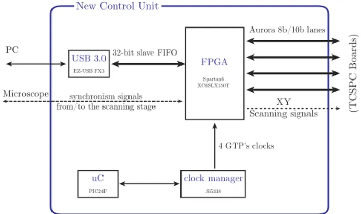
We completely re-designed the control unit, moving from a simple passive-HUB structure to a centralized-logic archi-tecture, which makes the system suitable for TCSPC scanning applications that could not be addressed before. In Fig.1, the structure of the new control unit is depicted.
A Spartan 6 FPGA by Xilinx is the central logic of the TCSPC system. It has to communicate with the four TCSPC boards in order to start/stop the acquisition and to download the recorded photons.
In order to fully exploit the conversion speed of the TAC, which can be connected to detectors counting up to 4 Mcps, data transfer from the TCSPC boards to the central FPGA has to be carefully designed. Considering the TACs operating at 4 Mcps, 14-bit conversions, 5-bit detector’s address, each TCSPC board generates a throughput of 608 Mbits/s; there-fore, the central FPGA has to manage an overall throughput up to 2.4 Gbits/s, in order not to limit the count rate. To ful-fill such a large band requirement, we decided to employ the FPGA’s GTP transceivers along with the 1.2 Gbits/s Aurora 8b/10b protocol by Xilinx for each connection. The designed Aurora lanes prevent the link between the CU and the TCSPC boards from limiting the count rate, but the central FPGA has
FIG. 1. Structure of the new control unit. Measurements done by the TCSPC boards are downloaded into the CU by means of four 1.2 Gbits/s 8b/10b Aurora lanes by Xilinx. The control unit collects recorded photons from an entire pixel and sends them to the PC through a USB 3.0 connection.
to properly deal with such a high throughput when manag-ing the acquisition of the frame, sortmanag-ing photons recorded in different pixels, and managing the communication with the host PC.
In order to not limit the count rate of the system, also the data transfer towards the host PC has to be taken into account. For this, a USB 3.0 connection has been chosen since it outperforms USB 2.0 and it is widely available. An EZ-USB FX3 device by Cypress manages the communication to the PC, handling the USB protocol, and communicates to the FPGA by means of a 32-bit parallel interface, called slave first-in-first-out (FIFO).
The central FPGA is also in charge of interfacing with a microscope, acquiring the synchronization signals provided by it, or directly driving the scanning stage. The central FPGA generates the properly phased signals to synchronize the oper-ation of TCSPC boards with respect to each other and to synchronize the TCSPC measurement with the moving of the scanning mirror. Finally, a microcontroller manages the power-up of the system and configures a programmable clock generator which provides the FPGA’s transceiver with the clock required for implementing the four 1.2 Gbits/s Aurora 8b/10b links.
III. FIRMWARE
Firmware has been developed for both the TCSPC boards and the control unit. The former ones have to perform the TCSPC measurement, timing photons synchronously with the scanning of the microscope, whereas the latter one has to collect all recorded photons and send them to the PC.
The main requirement was to perform a 256 × 256 scan image, with a pixel dwell time of 4 µs, 12-bit time resolution, and a maximum count rate of 4 Mcps/detector.
One issue that has to be faced when designing the sys-tem is the required throughput. Considering our application’s requirements, if each photon were tagged with the 5-bit detec-tor address, the data throughput toward the host PC would be 272 MB/s. All the generated data have to be collected by the PC and either stored onto a disk or processed in real-time. Managing such a high throughput is feasible but not trivial. For this reason, we decided to move to a different approach. Since the maximum required count rate is 4 Mcps and the pixel dwell time is 4 µs, a maximum of 16 photons can be recorded per detector per pixel (i.e., in a pixel dwell time). We decided to download a fixed number of events per detector per pixel, and this number has been set to 16. If the number of actual recorded photons by a detector is less than 16, addi-tional fake photons are created for padding. Those padding photons are time-tagged with the longest time delay (0xFFF), which therefore cannot be employed for real conversions, and then discarded by the processing software. In this way, having a fixed number of events per detector, we can avoid tagging the address of the fired detector, since it can be inferred by the photon position inside downloaded data, i.e., the first 16 events will always be related to detector #1, the second ones to detector #2, and so on. If the 5-bit detector address is not carried out, the throughput to the host PC is 192 MB/s, which is 30% less than the previous one.
The main drawbacks of this approach are twofold. First, if the average number of actual recorded photons per pixel is less than 16, the throughput is higher than what is needed and therefore there is a waste in band communication. This hap-pens for a detector rate less than 2.8 Mcps. If this were the case, the firmware could be easily modified to tag each pho-ton with the corresponding detector’s 5-bit address. Even if there is a lack of efficiency in the transmission for count rates less than 2.8 Mcps, it is worth noting that sending a fixed-dimension packet, independent of the count-rate, makes the transmission protocol and software post-processing simpler. The second limitation is that the 16-photon limit can cause a saturation of the acquired image. This is likely to be the case if the pixel scan time is greater than 4 µs. The limitation can be easily overcome by increasing the number of pixels per line and performing a pixel-binning in software post-processing. For instance, if the pixel dwell time is 8 µs, we can subdi-vide the line in 512 pixels (4 µs dwell time) instead of just 256. The acquired pixels are then binned two by two. At the end, the total number of effective pixels is again 256, but this time the equivalent threshold for the number of recorded photon is 32.
A. TCSPC board firmware
In Fig. 2, a block scheme of the TCSPC-board main FPGA’s firmware is illustrated.
The main tasks that the developed firmware accomplishes are three: acquisition management, pixel handling, and data transmission.
As soon as the TAC asserts a STROBE, signaling that a valid conversion has been performed, the FPGA samples the corresponding ADC output, issues a reset to the TAC, compensates the sliding-scale dithering, and sets the bin size. The high-performance on-board ADC features a 14-bit reso-lution,13 but the target application requires only 12 bits. We decided to let the user decide the bin size, i.e., which 12-bit subgroup to download per each ADC conversion. If the bin size is preserved, the 12 less significant bits are downloaded; if the bin size is doubled, bits from 12 to 1 are downloaded, whereas if the bin size is quadrupled, the 12 most significant bits are downloaded. The recorded photons are then saved into a First-In-First-Out (FIFO) memory, called channel FIFO. Inside the acquisition pipeline, also the number of recorded events is updated, to stop the recording process as soon as the 16-photon limit has been reached. The number of actual recorded events per pixel is also saved in a register to perform the padding.
Each TCSPC board employs two scanning signals com-ing from the control unit to synchronize the acquisition with the motion of the microscope’s scanning mirrors. The first signal is the pixel clock, which times the photon recordings into pixels. The second one is an enable signal, which is used for gating the acquisition when the scanning mirror ends a line and performs a carriage return. The system is designed either to receive the synchronization signals from the micro-scope or to directly drive the scanning stage. In the target application, the microscope was the master of the scanning procedure.
083704-4 Peronio et al. Rev. Sci. Instrum. 88, 083704 (2017)
FIG. 2. Schematic representation of the firmware developed for the four eight-channel TCSPC boards. The firmware accomplishes three main tasks: acquisition management, pixel handling, and data transmission to the CU.
The second task performed by the TCSPC firmware is pixel handling. A Finite-State-Machine (FSM), called pixel wrapping FSM, is triggered by the pixel clock and groups all photons recorded during the previous pixel period. The FPGA downloads photons from each channel FIFO sequen-tially and saves them into another FIFO, called transmission FIFO. Before reading the channel FIFOs, the pixel wrapping FSM reads the content of the registers in which the actual number of recorded photons is saved, in order to download the effective number of events and perform the padding if necessary.
Finally, the transmission FSM manages the download to the control unit by means of the 1.2 Gbits/s Aurora 8b/10b lane.
B. Control unit firmware
In Fig.3, the block scheme of the control unit FPGA’s firmware is reported.
The main tasks of the developed firmware are threefold. First it has to collect recorded photons coming from the TCSPC boards, group them into corresponding pixels, and send them to the FX3. Second, it has to receive commands from the PC, decode them, and send them to the TCSPC boards. Third, it has to receive/send synchronization signals from/to the microscope and manage the generation of the synchronization signals for the TCSPC boards.
Photons recorded by each TCSPC board are stored in a FIFO called buffer 1 FIFO. As soon as an entire pixel is stored in this memory, the channel sorting FSM reads it, re-arranges the order of photons, and saves them into a second FIFO, called buffer 2 FIFO. The reason for the sorting is that the detector address its different from the TCSPC chain address due to chal-lenges in Printed Circuit Board (PCB) layout, i.e., SPAD #1 is not routed to the first TAC of board #1. If a sorting is not done, the order of the recorded photons will not reflect the detector order. This is not an issue if the counts of different detectors are summed up, as in the case of the fluorescence lifetime imaging
microscopy (FLIM) image reported in Fig.6, but it is crucial if the photons recorded by different detectors have to be kept sep-arated as in the case of spectrally resolved imaging, where each detector of the linear array is used to acquire a different wave-length. Obviously the sorting can be done in software, but we decided to implement it in firmware to simply the post process-ing done by the end user. For this, two different sortprocess-ings have to be accomplished: the first one at single-board level, rearrang-ing the channel order inside a srearrang-ingle board, which is done by the channel sorting FSM, and the second one at the overall-board level, rearranging the board order, which is done by the pixel wrapping FSM. This FSM reads the buffer 2 FIFOs as soon as they contain all the photons recorded in a same pixel, performs the overall-board-level sorting, and saves them into the FX3 FIFO. If the FX3 FIFO has not enough space to store an entire pixel, all the photons are discarded. In this way, the download alignment is preserved, since it relies on the fact that a fixed number of photons have to be downloaded per each pixel. The pixel wrapping FSM adds a control word at the begin-ning of each pixel in which the pixel number and some error flags are stored. The PC software can therefore sort photons and reconstruct the image based on the pixel number reported by the control word. It is worth noting that if the PC exhibits latency, the FX3 FIFO saturates, and therefore some pixels can be lost. Some tests have been done acquiring several consec-utive frames and most of them were intact. If a frame presents some missing pixels, even if typically less than 1% of the total, it is discarded by the acquisition software. Finally, the FX3 handling FSM manages the communication from/to the FX3 device, sending the recorded photons and saving the incoming commands.
The decoding FSM decodes the incoming commands, which are then sent to the TCSPC boards too, by means of the Aurora 8b/10b lanes, managed by the transmission FSM. As for the management of the scanning procedure, a synchro-nization FSM handles all the alignment process, and it is able both to send the driving signals to the scanning mirror stage of the microscope and to receive and process them.
FIG. 3. Block scheme of the control unit firmware. The main tasks of the CU firmware are pixel handling, i.e., group the recorded photons into corresponding pixels, download data to the PC, receive and decode commands from the PC, and manage the synchronism signals for the scanning.
Regarding the targeted application, the microscope (a TCS SP8-X from Leica) is the master of the scanning procedure and it continuously scan 256 lines of the sample, each one com-posed by 256 pixels. The microscope has its own trigger box which generates the synchronization signals for the acquisi-tion logic. These signals are essentially two: line active and frame active, whose active levels signal that the microscope is scanning a line and a frame, respectively (see Fig.4).
The synchronization FSM captures those signals and gen-erates 256 pixel-clock periods per each line, based on the pixel period duration selected by the user. A replica of the line active is also generated (enable scan) as an enable signal to gate the acquisition as soon as the scanning stage ends the
FIG. 4. Synchronization signals used during a scanning. Frame active and line active are output by the microscope and they are high when the laser is scanning a line and a frame, respectively. Pixel clock and enable scan are generated by the FPGA. The former is used to divide the acquisition into pixels and it is delayed by a finite time Td with respect to the line active signal. The latter is synchronous with the pixel clock and it is a delayed replica of the line active signal that is used by the TCSPC boards to gate the acquisition when the laser is performing a carriage return.
line and performs a carriage return. Due to mechanical tol-erances, the line active signal could be not perfectly aligned with respect to the scanner position. Therefore, the acquired image would be off-centered and present a shift between adja-cent lines if the bidirectional scanning mode is performed. Moreover, the lifetime image would be off-centered also with respect to the intensity image acquired by the microscope’s internal detectors. To solve this issue, the synchronization FSM lets the user configure a fixed delay between the gen-erated enable signal and the first pixel-clock edge of the line (Td in Fig.4).
IV. EXPERIMENTAL RESULTS
The main goal of the project was to build a prototype that would be able to use fluorescence lifetime measure-ments to distinguish various stages of aggregation of alpha synuclein (aSyn) in cells. aSyn is a small, natively unstruc-tured protein that can aggregate into insoluble structures that are toxic to neurons, a phenomenon closely linked to the pathology of Parkinson’s disease.14 Our system should enable the direct measurement of the efficacy of aggregation-inhibiting drugs. The developed system was tested at the Institute for Biomedicine (Eurac Research—Bolzano) to validate the design and prove its suitability for scanning applications.
The system was connected to a TCS SP8-X confocal laser scanning microscope from Leica. The 32 SPADs were used as one single detector by collecting the light coming from the same spot and grouping together the corresponding timing
083704-6 Peronio et al. Rev. Sci. Instrum. 88, 083704 (2017)
FIG. 5. IRFs of the 32 channels after compensating mismatches with the calibration procedure. The different SNR are due to variations in the detectors’ dark count rates and to the non-uniform distribution of the light. The bump that is visible at 10 ns is due to optical cross talk, i.e., avalanches triggered by the secondary emission of photons of adjacent detectors.16
measurements to increase the count rate and therefore reduce the measurement time. In order to gather measurements done with different channels (SPAD + TAC), a calibration proce-dure is mandatory to compensate for mismatches, i.e., offsets and mean bin widths of the TCSPC chains are slightly dif-ferent. We employed an offline calibration, done by software on the recorded events, based on the algorithm proposed by Peronio et al.15
We tested the validity of the calibration procedure by acquiring the instrument response function (IRF) of the sys-tem for all the 32 detectors. The laser source integrated in the SP8-X is a supercontinuum laser by NKT that was tuned at 488 nm with a repetition rate of 40 MHz and the full-scale range of the TACs was set to 25 ns accordingly. In Fig.5, the 32 measured IRF are reported after being calibrated. As it can be seen, the alignment is good, i.e., the maximum shift among the peaks is less than the 63-ps jitter of the detectors; there-fore, measurements performed with different channels can be effectively grouped together without significantly impairing the performance.
In order for the detectors to collect the light coming from the same spot, a proper beam shaping optical system has been
used. The light coming from the pinhole of the microscope was focused onto the array by means of a cascade of four lenses: the first lens was used to collimate the divergent beam; the second and the third ones were coupled and used as a beam expander to make the section of the beam fit the linear dimension of the array; the last one is a cylindrical lens and it was used to focus the beam down to a dimension of ∼50 µm only in one axis, to fit the dimension of the detector. It is worth noting that even if the fill factor of the linear array is limited to 16.11%, there is still a reduction in the measurement time by using 32 detectors in parallel. Moreover, the module has been conceived to work in conjunction with a microlens array, i.e., the pixel pitch has been set to 250 µm, to match a typical pitch of commercial lenses, which can increase the fill factor to 80%.
A Convallaria test sample from Leica was also imaged to characterize the system. The light impinging on the sam-ple was filtered with the built-in acousto-optical tunable filter (AOTF) of the microscope selecting the 488-nm wavelength. The fluorescence light was directed through a pinhole, filtered with a 488-nm notch filter to remove residual laser light, and then focused onto the detector array.
Figure6shows 256 × 256 images obtained from the test sample. Both the intensity image (a) and the FLIM image (b), obtained after processing the acquired histograms with the FLIMfit software, are shown. Ninety frames were acquired and summed with a scan rate of 1 frame/s, which corresponds to a pixel dwell time of about 4 µs. The actual total dwell time was much less than 90 s (about 22 s) since the scanner spent most of the time in carriage returns; therefore, the mean download rate was also reduced by a factor of ∼4, i.e., 50 MB/s, but the peak rate was about 192 MB/s, as expected. In this particular case, a slower scan could be performed instead of superimpos-ing 90 frames, but in general our target was the possibility of resolving and analyzing different frames, in order to be able to study a temporal evolution of the sample conditions. In TableI, a summary of both the theoretical and the effective through-put is reported. Finally, two main lifetimes are visible in the sample: the first around 600 ps, whereas the second is around 2.3 ns.
In Fig.7, two histograms are reported with the correspond-ing measured IRFs. Those histograms have been acquired in the two areas highlighted in Fig.6(b)(white circles). A binning of 4 × 4 pixels has been performed.
FIG. 6. (a) Intensity image, (b) FLIM image. Two main lifetimes are visible in the FLIM image: the first around 600 ps and the second around 2.3 ns.
TABLE I. Summary table of the throughput.
Pixel dwell time 4 µs
Image size 256 × 256
Theoretical frame rate (no carriage return) 4 frame/s Theoretical throughput (no carriage return) 192 MB/s
Effective frame rate 1 frame/s
Effective average throughput 50 MB/s
Effective peak throughput 192 MB/s
Finally, in Fig.8, to demonstrate the effectiveness of the system, a plot of the number of frames needed to acquire 1000 photons/pixel as a function of the number of detectors used in parallel is reported. The threshold of 1000 photons has been chosen to estimate the lifetime with an accuracy of few percent.17The blue line represents the actual scenario and it has been obtained with the following procedure. First, we selected a particular pixel of the image reported in Fig.6(b)and extracted the average number of photons recorded per frame in that pixel by each detector. Then, we calculated how many frames were necessary to accumulate 1000 photons if (i) only SPAD #1 were used, (ii) SPAD #1 and #2 were used, (iii) and so on. The red line represents the ideal case, with the number of frames inversely proportional to the number of detectors working in parallel. In this case, we used the average num-ber of counts recorded per frame by SPAD #1 to calculate the number of frames needed using only one detector. The other points of the plot were drawn by decreasing the number of frames proportionally with the number of detectors employed. The difference between the two curves is due to the fact that the light was not uniformly distributed over the SPAD array, and indeed the detector’s count rate was higher in the cen-tral region and decreased moving towards the edges. As it can be seen, the system effectively reduces the measurement time. In this case, there is a reduction by a factor of 17, which can be further improved towards the limit of 32 by using bet-ter optics and a microlens array. It is worth noting that the effective increase in the recorded efficiency has been obtained by increasing the level of parallelism of both the detector and the timing electronics. For instance, the same gain is not
FIG. 8. Number of frames needed to acquire 1000 photons as a function of the number of detectors used in parallel. The blue line represents the actual scenario, whereas the red line represents the ideal scenario where the number of frames is inversely proportional to the number of detectors working in parallel.
achievable by only employing a SPAD with an area 17 times bigger. Indeed, the bigger SPAD would collect 17 times more photons, but the recorded number of events would not increase accordingly due to the finite dead time of both the detector and acquisition logic. Moreover, the count rate of the single detector has to be limited to avoid classic pile-up.
On the other hand, even a 17 times faster laser cannot increase the number of photons in the same way, since the recorded rate would be limited by the dead time also in this case. Moreover, a 17 times faster laser would also have a 17 times shorter period, which is too short for detecting a lifetime of few nanoseconds.
Conversely, an effective increase in the count rate can be obtained by increasing the parallelism level of the system in order to either strongly reduce the dead time18or manage several independent acquisition chains.19It is worth noting that both these last two solutions have been developed exploiting the CMOS technology to increase the level of integration, but they do not match the best state-of-the-art performance from neither the detector nor the timing electronics.
FIG. 7. Acquired histograms and normalized IRF for two different areas of the sample: (a) with a mean lifetime around 600 ps, (b) with a mean lifetime around 2 ns.
083704-8 Peronio et al. Rev. Sci. Instrum. 88, 083704 (2017) V. CONCLUSIONS
In this paper, we present the re-design of a 32 × 1 complete TCSPC module. The new module was developed specifically targeting scanning applications, which could not be addressed with a previously developed version, mainly due to a lack of a centralized architecture. The main goal of this work was to move from a proof of concept towards a system that could be effectively integrated in an imaging setup.
Preliminary tests with biological samples have been car-ried out at the Institute for Biomedicine at Eurac Research, and the results have validated the new system, which can therefore be routinely employed in life science scanning applications.
ACKNOWLEDGMENTS
This work was supported by the Provincia Autonoma di Bolzano under the MULTISCREEN project.
1H. Studier, K. Weisshart, O. Holub, and W. Becker,Proc. SPIE8948,
89481K (2014).
2W. Becker, A. Bergmann, G. Biscotti, K. Koenig, I. Riemann, L. Kelbauskas,
and C. Biskup,Proc. SPIE5323, 27 (2004).
3W. Becker, A. Bergmann, H. Wabnitz, D. Grosenick, and A. Liebert,Proc.
SPIE4431, 249 (2001).
4W. Becker, Advanced Time-Correlated Single Photon Counting Techniques
(Springer, Berlin, 2005).
5Becker & Hickl, Four-Channel Time-Correlated Single Photon Counting
Package, SPC-154.
6PicoQuant, Multichannel Picosecond Event Timer and TCSPC Module with
USB Interface, HydraHarp 400.
7R. M. Field, S. Realov, and K. L. Shepard,IEEE J. Solid-State Circuits49,
867 (2014).
8M. Gersbach, Y. Maruyama, R. Trimananda, M. W. Fishburn, D. Stoppa,
J. A. Richardson, R. J. Walker, R. K. Henderson, and E. Charbon,
IEEE J. Solid-State Circuits47, 1394 (2012).
9N. Krstaji´c, S. Poland, J. Levitt, R. Walker, A. Erdogan, S. Ameer-Beg, and
R. K. Henderson,Opt. Lett.40, 4305 (2015).
10C. Veerappan, J. A. Richardson, R. J. Walker, D. D. Li, M. W. Fishburn,
Y. Maruyama, D. Stoppa, F. Borghetti, M. Gersbach, R. K. Henderson, and E. Charbon, in 2011 IEEE International Solid-State Circuits Conference, San Francisco, CA (IEEE, 2011), p. 312.
11J. Lapington, T. Ashton, D. Ross, and T. Conneely,Nucl. Instrum. Methods
Phys. Res., Sect. A695, 78 (2012).
12A. Cuccato, S. Antonioli, M. Crotti, I. Labanca, A. Gulinatti, I. Rech, and
M. Ghioni,IEEE Photonics J.5, 6801514 (2013).
13S. Antonioli, L. Miari, A. Cuccato, M. Crotti, I. Rech, and M. Ghioni,
Rev. Sci. Instrum.84, 064705 (2013).
14G. S. K. Schierle, C. W. Bertoncini, F. T. S. Chan, A. T. van der
Goot, S. Schwedler, J. Skepper, S. Schlachter, T. van Ham, A. Espos-ito, J. R. Kumita, E. A. A. Nollen, C. M. Dobson, and C. F. Kaminski,
ChemPhysChem12, 673 (2011).
15P. Peronio, G. Acconcia, I. Rech, and M. Ghioni,Rev. Sci. Instrum.86,
113101 (2015).
16I. Rech, A. Ingargiola, R. Spinelli, I. Labanca, S. Marangoni, M. Ghioni,
and S. Cova,IEEE Photonics Technol. Lett.20, 330 (2008).
17M. K¨ollner and J. Wolfrum,Chem. Phys. Lett.200, 199 (1992).
18N. A. W. Dutton, S. Gnecchi, L. Parmesan, A. J. Holmes, B. R. Rae,
L. A. Grant, and R. K. Henderson, in 2015 IEEE International Solid-State Circuits Conference, San Francisco, CA (IEEE, 2015), p. 204.
19F. Villa, R. Lussana, D. Bronzi, S. Tisa, A. Tosi, F. Zappa, A. Dalla Mora,
D. Contini, D. Durini, S. Weyers, and W. Brockherde,IEEE J. Sel. Top. Quantum Electron.20, 364 (2014).