Proceedings 2018, 2, 892; doi:10.3390/proceedings2130892 www.mdpi.com/journal/proceedings Proceedings
InGaN/GaN nanoLED Arrays as a Novel
Illumination Source for Biomedical Imaging
and Sensing Applications
†Jan Gülink 1,*, Steffen Bornemann 1, Hendrik Spende 1, Matthias Auf der Maur 2, Aldo Di Carlo 2,
Joan Daniel Prades 3, Hutomo Suryo Wasisto 1,* and Andreas Waag 1
1 Institute of Semiconductor Technology (IHT) and Laboratory for Emerging Nanometrology (LENA), Technische Universität Braunschweig, D-38106 Braunschweig, Germany; [email protected] (S.B.); [email protected]@tu-braunschweig.de (H.S.); [email protected]@tu-braunschweig.de (A.W.) 2 Department of Electronic Engineering, Universitá degli Studi di Roma “Tor Vergata”, I-00133 Rome, Italy;
[email protected] (M.A.d.M.); [email protected] (A.D.C.)
3 MIND-IN2UB, Department Electronic and Biomedical Engineering, University of Barcelona, E-80124 Barcelona, Spain; [email protected]
* Correspondence: [email protected] (J.G.); [email protected] (H.S.W.); Tel.: +49-531-391-3814 (J.G.); +49-531-391-3167 (H.S.W.)
† Presented at the Eurosensors 2018 Conference, Graz, Austria, 9–12 September 2018. Published: 6 December 2018
Abstract: Guidelines for the fabrication of nanoscale light-emitting diode arrays (i.e., nanoLED
arrays) based on patterned gallium nitride (GaN) with very small dimensions and pitches have been derived in this work. Several challenges during top-down LED array processing have been tackled involving hybrid etching and polymer-based planarization to yield completely insulated highaspect-ratio LED fin structures and support the creation of p-GaN crossing line contacts, respectively. Furthermore, simulations of the light emission patterns were also performed providing hints for enhancing the device designs. As a result, regardless of the required device processing optimization, the developed nanoLED arrays are expected to offer high potential as novel illumination sources in biomedical imaging and sensing applications (e.g., mini compact microscopes and wearable biological/chemical nanoparticle counters)
Keywords: gallium nitride; LED; micro LED; LED array; nanofin; hybrid etching; illumination
source
1. Introduction
Starting from the invention of the planar blue GaN LEDs in the early 1990s [1], the LED technology has emerged over the last three decades as highly efficient, compact, and robust light sources. While the device development at the beginning was concentrated only on solid-state lighting, the focus has shifted in recent years to more broadened applications (e.g., optical communication, sensing and manipulation in life sciences, and structured illumination). By integrating GaN LEDs with CMOS control electronics, matrix-addressed and individually controlled microLED arrays were realized with a display luminance as high as 106 cd/m2 (12 W/cm2), which is a
factor of 103 higher than normal commercial displays [2]. Although these optoelectronic devices
exhibited promising results and could subsequently be used for illumination sources and manipulation tools in the life sciences, their spatial resolution was still low, which resulted from LED dimensions with pixel and pitch sizes in the range of several tens to hundreds of micrometers, respectively. Thus, further miniaturization will enable the use of such nanoLED arrays as a basis for novel imaging and sensing techniques.
Therefore, in this paper, we report on a novel illumination source based on high-aspect-ratio nanofins directly etched from an InGaN/GaN LED wafer with the aim to realize highly localized light sources with pixel sizes in the range of the wavelength and individual pixel control. In contrary to conventional microscopy that has an optical resolution limit depending on the used detection system or sensor, the developed nanoLED matrix will pave the way for chip-based lensless microscopy, in which the spatial resolution is defined by the size of illumination source. Therefore, well-controlled and reproducible 3D device processing steps are necessary to be developed.
2. Device Concept and Simulation
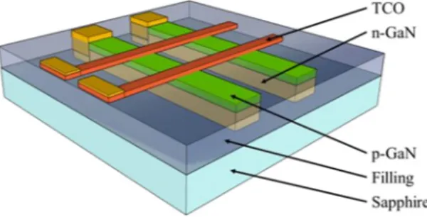
The production of the GaN nanoLED arrays are based on a series of top-down processing steps, consisting of nano-photolithography, hybrid etching (i.e., combination of dry and wet etching methods), planarization, and metal contact line creation. A schematic of a matrix-addressed LED array is depicted in Figure 1. From this design, it is obvious that 3D nanoarchitectures and processing will be involved during the device fabrication, in which the trenches between high-aspect-ratio etched structures need to be perfectly planarized in order to be able to realize very small and parallel metal contact lines on their top.
Figure 1. 3D schematic of a simplified 2 × 2 LED array based on fins etched from a planar LED wafer. Matrix-addressing of each LED pixel is obtained by n-GaN bottom contact via each fin and p-GaN crossing line contact on top of the planarized fins made of either a transparent conductive oxide (TCO) or a semitransparent thin metal stack.
The feasibility of a matrix-addressed approach based on fin structures is evaluated with simulations. In this case, several concerns have been raised as the devices were scaled down to submicron sizes (e.g., light emission pattern, crosstalk between the LED pixels, and different conditions of top p-GaN contact). Therefore, the simulations have been used to define general guidelines for the fabrication of the nanoLED array. The simulations were conducted with COMSOL Multiphysics 5.3. To start the investigation, an array of 11 fins with a width of 1 µm and a pitch of 3 µm was created as a basis model for the simulation. A point dipole located at the center of the middle fin and in the height of the multi quantum well (MQW) was chosen and set to simulate the initial point of emission. From the simulations results, it was found that various geometries, wavelengths, and material arrangements will result in different light emission patterns (c.f. Figure 2).
Figure 2. Simulation results of LED array comprising 11 fins with a width of 1 µm and a dipole emission at 450 nm from the middle fin. Localized top emission can be obtained from the LED fin (a) without top contact. LED fin with connecting ITO p-contact line showing optical crosstalk and widened side lobes (b).
3. Device Fabrication
The fabrication of nanoLED array can be divided into four main processing steps (i.e., n-contact
opening and definition, fin formation, filling for planarization, and creation of p-contact lines and bond wire pads). First, the device manufacturing starts with the photolithography to create the area for the
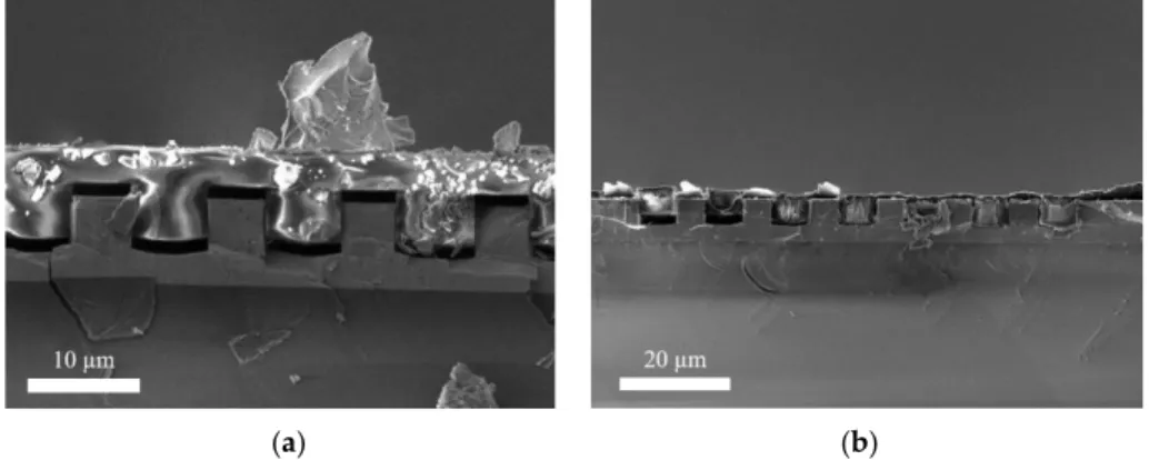
etching process down to n-GaN, which is around 1.2 µm deep from the initial top p-GaN surface. In this case, rectangular patterned chromium with a thickness of 300 nm was used as a mask followed by inductively coupled plasma dry reactive ion etching (ICP-DRIE) to reach the highly n-doped regime of the LED wafer. Afterwards, the 3D GaN fin LED arrays were created by means of hybrid etching combining both SF6/H2-based ICP-DRIE and KOH-based post-wet chemical etching. It should be noted that the 500 nm thick chromium deposited via electron beam evaporation and partially removed by lift-off was necessary to be used as hard etching mask instead of only photoresist like in Si-based etching [3] due to GaN hardness. To obtain high-aspect-ratio GaN structures with smooth sidewalls and to guarantee insulation among the fins, two-step hybrid etching was employed, which is an enhancement from our previous GaN nanowire etching technique [4,5]. In this case, the first and the second ICP-DRIE steps have etch durations of 45 min and 30 min, respectively. Meanwhile, the wet etching using AZ 400 K developer was kept at the same etch time of 1 h for both steps. The fabricated fin arrays with a width of 1 µm, a pitch of 2 µm and a height of 5 µm are depicted in Figure 3. The quality of the MQW was thereafter determined with cathodoluminescence measurements and showed no deterioration due to the etching procedure.
The third step comprises the filling and planarization of the fin structures. The aim is to introduce a flat surface again, so that the next lithography step is possible and to reveal the top facets of the fin structures enabling the p-contact. The polymer benzocyclobutene (BCB) from The Dow Chemical Company (i.e., CYCLOTENE 3022-57) was employed as filling material. In terms of its dielectric characteristic, this material is considered as an isolating low-k material (εr = 2.65), which can be spun on the wafers and subsequently etched with inductively coupled plasma (ICP) dry etching method [6]. The conditions of the samples after BCB filling and its subsequent ICP etching are depicted in Figure 4a,b, respectively. This planarized wafer is the basis for the p-contact deposition to complete the fabrication of the device.
(a) (b)
Figure 4. Cross section of planarized fins directly after spin-on and hard bake (a) and ICP etching (b). The trenches are filled adequately.
4. Conclusions
A matrix-addressed approach for LED arrays based on nanofins has been proposed and developed to be used for novel illumination source, which allows to achieve pixel sizes of down to below 1 µm and pixel pitches of 1–2 µm. The fin formation is possible with optical lithography and etching methods and therefore suitable for higher volume fabrication. The filling process with BCB and its height adjustment via ICP etching, which are highly dependent on geometries of underlying structures, have been optimized for the designed structures. Future work will focus on semitransparent thin metal or TCO deposition as well as the characterization of the optoelectronical properties of the developed devices.
Author Contributions: J.G. designed and conducted the experiments; M.A.d.M. and A.D.C. performed the simulations; J.G. and S.B. analyzed the data; H.S. contributed on analysis tools; J.D.P., H.S.W. and A.W. had a supervisory role; J.G. wrote the paper; H.S.W. revised and provided inputs for writing improvement; All authors read and agreed on the written paper.
Acknowledgments: This work has been partially performed within LENA-OptoSense funded by the Lower Saxony Ministry for Science and Culture (N-MWK), European project of ChipScope funded by the European Union’s Horizon 2020 research and innovation program under grant agreement no. 737089, and the joint collaboration of Epitaxy Competence Center (ec2), funded by Osram Opto Semiconductors GmbH.
Conflicts of Interest: The authors declare no conflict of interest.
References
1. Nakamura, S.; Senoh, M.; Iwasa, N.; Nagahama, S.I. High-brightness InGaN blue, green and yellow light-emitting diodes with quantum well structures. Jpn. J. Appl. Phys 1995, 34, L797–L799.
2. Herrnsdorf, J.; McKendry, J.J.; Zhang, S.; Xie, E.; Ferreira, R.; Massoubre, D.; Zuhdi, A.M.; Henderson, R.K.; Underwood, I.; Watson, S.; et al. Active-matrix GaN micro light-emitting diode display with unprecedented brightness. IEEE Trans. Electron Devices 2015, 62, 1918–1925, doi:10.1109/TED.2015.
3. Wasisto, H.S.; Merzsch, S.; Steib, F.; Waag, A.; Peiner, E. Vertical silicon nanowire array-patterned microcantilever resonators for enhanced detection of cigarette smoke aerosols. Micro Nano Lett. 2014, 9, 676–679.
4. Yu, F.; Yao, S.; Römer, F.; Witzigmann, B.; Schimpke, T.; Strassburg, M.; Bakin, A.; Schumacher, H.W.; Peiner, E.; Wasisto, H.S.; et al. GaN nanowire arrays with nonpolar sidewalls for vertically integrated fieldeffect transistors. Nanotechnology 2017, 28, 95206, doi:10.1088/1361-6528/aa57b6.
5. Yu, F.; Strempel, K.; Fatahilah, M.F.; Zhou, H.; Römer, F.; Bakin, A.; Witzigmann, B.; Schumacher, H.W.; Wasisto, H.S.; Waag, A. Normally Off Vertical 3-D GaN Nanowire MOSFETs With Inverted -GaN Channel. IEEE Trans. Electron Devices 2018, 65, 2439–2445, doi:10.1109/TED.2018.2824985.
6. Woehrmann, M.; Toepper, M. Polymerization of Thin Film Polymers. In New Polymers for Special
Applications, 1st ed.; Ailton De Souza Gomes, IntechOpen: Rijeka, Croatia. 2012; doi:10.5772/48205. © 2018 by the authors. Licensee MDPI, Basel, Switzerland. This article is an open access article distributed under the terms and conditions of the Creative Commons Attribution (CC BY) license (http://creativecommons.org/licenses/by/4.0/).