Alma Mater Studiorum · University of Bologna
School of Science
Department of Physics and Astronomy Master Degree in Physics
Quality investigation of an ATLAS Phase-II
DAQ board via Signal Integrity simulations
Supervisor:
Prof. Alessandro Gabrielli
Co-supervisor:
Ing. Luca Pelliccioni
Ing. Roberto Carretta
Submitted by:
Marco Collesei
"Siate felici,
e se qualche volta la felicità si scorda di voi,
voi non vi scordate della felicità."
- Roberto Benigni
Abstract
The desire of discovering the unknown features of the Universe has always been the driv-ing force of particle physicists. Through particle colliders of increasdriv-ing performances, over almost five decades of research in High Energy Physics (HEP), many milestones of the Standard Model (SM), the most accurate and predictive theory of matter up to now, have been set. The impulse of achieving knowledge and finding answers to fundamental questions has lead to the construction of more and more large and powerful apparati. The Large Hadron Collider (LHC) is the most significant expression of the efforts of physicists all over the world and it is always under development to push its colliding and detection limits.
As a matter of fact, by the end of 2024 the installation work of a renewed collider, ca-pable of reaching a nominal luminosity of ∼7.5×1034 cm−2s−1, will take place. The new
apparatus, called High Luminosity-LHC (HL-LHC), will be operational at least for an-other decade and, to accomplish the challenges posed by the search for new physics, the main detectors such as A Toroidal LHC ApparuS (ATLAS) and Compact Muon Solenoid (CMS) will be upgraded for Phase-II.
Together with the structural changings in ATLAS sub-detectors, the entire Trigger and Data Acquisition (TDAQ) strategy will be upgraded by the implementation of new tech-nologies.
Among these technology advancements the FrontEnd LInk eXchange (FELIX) DAQ board, developed by Brookhaven National Laboratory (BNL) together with ATLAS, will play a prominent role. The new high-speed Printed Circuit Board (PCB) will handle the communication between the sub-detectors, the first level of trigger and the Dataflow, thanks to its multi Gb/s links and programmable logic, which makes the board a versa-tile and long-lasting element of the TDAQ chain.
My personal work has been testing some of the transmission channels of FELIX Phase-II board, in the light of Signal Integrity (SI), with the goal to supply simulation results confirming the reliability of its high data-rate lines. Ultimately, I have given evidence that high-speed digital design is a key step in DAQ boards research and development, and it is an essential instrument to reach optimal performances.
Contents
Introduction v
1 ATLAS experiment 1
1.1 LHC and ATLAS state of art . . . 2
1.1.1 LHC . . . 2 1.1.2 ATLAS . . . 3 1.2 Phase-II upgrade . . . 13 1.3 FELIX project . . . 21 2 Signal Integrity 27 2.1 Signal Integrity . . . 28 2.1.1 Transmission . . . 28 2.1.2 Main issues . . . 29 2.1.3 SI methodology . . . 32
3 Simulation with HyperLynx 35 3.1 Groundwork . . . 35 3.1.1 Models . . . 36 3.2 Results . . . 41 4 Increasing performances 45 4.1 Parameters . . . 47 4.1.1 Geometrical . . . 47 4.1.2 Configuration . . . 48 4.2 Proposed solution . . . 48 5 Conclusions 51 A FPGA 55
B Supplementary diagnostic diagrams 57
Introduction
Particle physics investigates the structure of matter and the mechanisms that govern the Universe. Since the late 50s, particle accelerators have been used by physicists all over the world to closely observe the nuclear and subnuclear reactions of fundamental bricks of Nature. These accelerators can be of various shapes and sizes, capable of ac-celerating particles to different energies. Over the decades, accelerated beam energies of gradually increasing orders of magnitude have been reached to better understand the phenomena described by the Standard Model (SM).
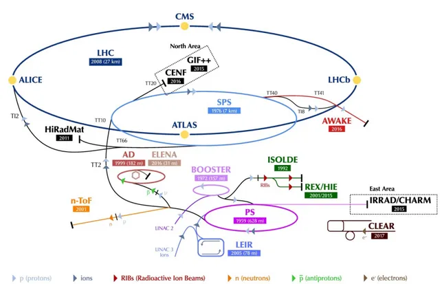
Near Geneva, is present and active the Conseil Européen pour la Recherche Nucléaire (CERN), the largest collaboration in the world of physicists, computer scientists and engineers. CERN hosts the Large Hadron Collider (LHC), the most powerful particle accelerator ever build, with a ring structure 27 km long and a center of mass energy of 13 TeV.
Four main detectors take place around LHC interaction points: A Toroidal LHC ApparuS (ATLAS), Compact Muon Solenoid (CMS), A Large Ion Collider Experiment (ALICE) and LHCb, which have the task of reconstructing, starting from the trajectories of the particles, the mechanisms underlying the fundamental interactions.
The current theory, described by the SM, predicts the existence of a defined number of elementary constituents subjected to fundamental forces mediated by other fundamental particles.
Despite the numerous confirmations and many predictions of the Standard Model ob-tained through experiments, nowadays there are still some open problems such as the unification of fundamental forces (GUT), the reconciliation between general relativity and quantum theory, the understanding of Dark Matter and Dark Energy and the de-termination of many SM parameters with increased accuracy.
To allow researchers to perform increasingly precise and meaningful experiments, the accelerators and all the measuring devices technologies are constantly updated. In par-ticular, the ATLAS experiment, as well as the other detectors present at CERN, will be updated in several phases, both in the structure of its sub-detectors and in the data acquisition electronics, to cope with the increasing luminosity and number of interactions per event.
Especially, with the major improvement from LHC to High Luminosity-LHC (HL-LHC) by the end of 2024, ATLAS sub-detectors performances will be enhanced with partial or entire substitution with new sub-systems. Together with these structural changes, and
since the produced amount of information will rise considerably, the whole Trigger and Data Acquisition (TDAQ) chain will be redesigned to accomplish Phase-II requirements. A basic component of the new TDAQ outline for Phase-II upgrade of ATLAS is the Front-End LInk eXchange (FELIX) board, which is the result of joint developing efforts of Brookhaven National Laboratory (BNL) and CERN. The idea behind the project is a high-speed, versatile, non-custom Printed Circuit Board (PCB) that can be programmed and upgraded to handle the trigger and the data received from the new Inner Tracker (ITk), the Calorimeters and the Muon System.
The object of study of this thesis is the quality of signal transmission on FELIX Phase-II acquisition board. In detail the work is articulated in four main chapters:
Chapter 1 is a detailed description of the actual status of LHC and the ATLAS experi-ment, with the attention posed to ATLAS Phase-II upgrade and the introduction of the FELIX project together with the main characteristics of the board.
Chapter 2 introduces the world of Signal Integrity (SI), in the optic of supplying the background of high-speed digital design, with related considerations and issues.
SI is the core of the investigation that I have driven on the FELIX Phase-II board; all the preliminary considerations that I have made on the project, and the following choices that I have taken, are based on the theory of high-speed signal theory.
Chapter 3is where the previous considerations are applied to the FELIX. Together with the technical support received from the Link Engineering of S.Giovanni in Persiceto (BO), in the person of Roberto Carretta as Signal And Power Integrity Analysis Spe-cialist and Luca Pelliccioni as Chief Technical Officer, and the collaboration of Bologna INFN section, I have lead the SI simulations on the board.
The aim of these simulations was to ensure the goodness of signal transmission over possible critical nets operating in the order of 10 Gb/s. As a matter of fact, all the simulations but one performed well, thus I have put particular attention to the only one that was affected by signal degradation.
Chapter 4 is the final expression of all the observations that have been made so far. I have proposed two successful solutions to restore the SI of the poor quality transmission line, identified in the first series of SI simulations, proving that the knowledge that I have acquired and the experience that I have made in this thesis work can provide an essential support to the new FELIX board development.
Chapter 1
ATLAS experiment
For several decades, particle colliders have been essential tools for particle physics. From the very beginning, such accelerators have been among the most complicated sci-entific instruments ever built, involving tens of thousands of scientists over the world. The Large Hadron Collider (LHC) is the most illustrative example of this technology. Among the past two decades, it has opened a new frontier in particle physics thanks to its high collision energy and luminosity.
One of its largest experiments, A Toroidal LHC ApparatuS (ATLAS), has been built guided by the principle of maximising the discovery potential for new physics, such as Higgs bosons and supersymmetric particles, while keeping the capability of high-accuracy measurements of known objects like heavy quarks and gauge bosons.
The basic design criteria of the detector include:
• a very good electromagnetic calorimetry for electron and photon identification and measurements, paired with full-coverage hadronic calorimetry for accurate jet and missing transverse energy measurements;
• high-precision muon momentum measurements, capable of measurements at the highest luminosity using the external muon spectrometer;
• efficient tracking at high luminosity for high transverse momentum measurements and full event reconstruction at lower luminosity;
• large acceptance in pseudorapidity (η) with almost full azimuthal angle (φ) coverage everywhere. φ angle is measured around the beam axis, whereas η relates to the polar angle θ (where θ is the angle from the z-direction);
• triggering and measurements of particles at low transverse momentum thresholds, providing high efficiencies for most physics processes of interest at LHC.
1.1
LHC and ATLAS state of art
Figure 1.1: CERN accelerator complex; the LHC in blue is the last stage of the acceler-ating chain which comprises smaller rings.
1.1.1
LHC
The LHC is a circular collider with 14 TeV centre of mass energy and design luminosity of 1034 cm−2s−1. Beam crossings are 25 ns apart and, at design luminosity, there are
23 interactions per crossing. It is supplied with protons and Pb ions from the existing injector chain comprising:
• the injector chain Linac2;
• Proton Synchrotron Booster (PSB); • Proton Synchrotron (PS);
• Super Proton Synchrotron (SPS).
The project, approved by CERN council in December 1994, took place into the under-ground infrastructure of Large Electron Positron (LEP) collider that consisted of a 26.7 km long ring tunnel. LEP included experimental areas at four points (2, 4, 6 and 8), each
1.1 LHC and ATLAS state of art 3
incorporating experimental and service caverns and, for the LHC project, the existing LEP tunnel has been re-used after the complete dismantling of the LEP machine. Besides, new structures have been added including experimental and service caverns destined to hold two new experiments. Of the four LHC experimental areas, two have been constructed on almost empty sites where there was very little existing infrastruc-ture. As such, two large experimental zones for ATLAS and CMS took place at points 1 and 5 respectively. For the two smaller experiments (ALICE and LHCb) the existing infrastructure has required only minor modifications to locate the new detectors.
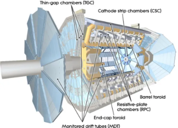
Figure 1.2: Open view of sub-detectors geometry in the ATLAS experiment, including the central solenoid magnet and the barrel and end-cap toroid magnets.
1.1.2
ATLAS
ATLAS experiment is a general-purpose detector designed to exploit the full discov-ery potential of the LHC. Many of the interesting physics questions at the LHC require high luminosity, and so the primary goal is to operate at a luminosity of 1034 cm−2s−1
with a detector that provides as many signatures as possible, using electron, photon, muon, jet, and missing transverse energy measurements, as well as b-quark tagging. The variety of signatures, both at low and high transverse momentum, is important in the high-rate environment of the LHC to achieve robust and redundant physics measure-ments. The detector was meant to achieve different physics goals such as:
• the search of the Higgs boson, which resent some of the most challenging signatures, involving high-resolution measurements of electrons, photons and muons, excellent secondary vertex detection for τ-leptons and b-quarks, high-resolution calorimetry for jets and missing transverse energy essential to explore the full range of possible masses;
• searches for SUSY at the electroweak scale with expected abundant production of squarks and gluinos leading to a variety of signatures involving multi-jets, leptons, photons, heavy flavours and missing energy;
• the precision measurements of the W and top-quark masses, gauge boson couplings, CP violation and the determination of the Cabibbo-Kobayashi-Maskawa unitarity triangle.
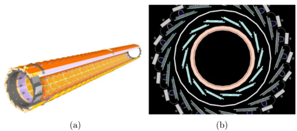
The dimensions of the ATLAS detector are remarkable, as a matter of fact the outer chambers of the barrel are at a radius of about 11 m. The half-length of the barrel toroid coils is 12.5 m, and the third layer of the forward muon chambers, mounted on the cavern wall, is located about 23 m from the interaction point. Also its weight is significant as the overall weight of the ATLAS detector is about 7000 tons. Large superconducting air-core toroid magnets surround a variety of sub-detectors here listed [1].
Muon spectrometer The conceptual layout of the muon spectrometer is based on the magnetic deflection of muon tracks. Over the range |η| ≤ 1.0, magnetic bending is provided by the large barrel toroid. For 1.4 ≤ |η| ≤ 2.7, muon tracks are bent by two smaller end-cap magnets inserted into both ends of the barrel toroid. Over 1.0 ≤ |η| ≤ 1.4 magnetic deflection is provided by a combination of barrel and end-cap fields.
Figure 1.3: Cross sections of the four technologies employed for muon detec-tion.
This magnet configuration provides a field mostly orthogonal to the muon trajectories. Trigger and reconstruction algorithms are op-timised to cope with the difficult background conditions resulting from penetrating primary collision products and from radiation back-ground produced from secondary interactions in the calorimeters.
In the barrel region, tracks are measured in chambers arranged in three cylindrical lay-ers around the beam axis; in the transition and end-cap regions instead, the chambers are placed vertically. Four chamber technologies, arranged such that particles from the interac-tion point traverse three stainterac-tions of chambers, are described below.
1.1 LHC and ATLAS state of art 5
MDT Monitored Drift Tubes (MDT) are aluminium tubes of 30 mm diameter and 400 µm wall thickness, with a 50 µm diameter central W–Re wire. The tubes are filled with a non-flammable mixture of 93% Ar and 7% CO2 at 3 bar of pressure, allowing a
maximum drift time of ∼700 ns, a small Lorentz angle, and excellent ageing properties with a single-wire resolution of ∼80 µm.
CSC Cathode Strip Chambers (CSC) are multi-wire proportional chambers with cathode strip readout and with a symmetric cell in which the anode-cathode spacing is equal to the anode wire pitch. The precision coordinate is obtained by measuring the charge induced on the segmented cathode by the avalanche formed on the anode wire. A good spatial resolution is obtained by segmenting the readout cathode and by charge interpolation between neighbouring strips. The anode wire pitch is 2.54 mm and the cathode readout pitch is 5.08 mm providing with position resolutions of better than 60 µm and small electron drift times (30ns), good time resolution (7 ns) and low neutron sensitivity. The gas mixture is a non-flammable mixture of 30% Ar, 50% CO2 and 20%
CF4, with a total volume of 1.1 m3.
RPC Resistive Plate Chambers (RPC) are a gaseous detector providing a typical space-time resolution of 1 cm × 1 ns with digital readout. The basic RPC unit is a narrow gas gap formed by two parallel resistive Bakelite plates, separated by insulating spacers. The primary ionisation electrons are multiplied into avalanches by a high, uniform electric field of typically 4.5 kV/mm and amplification in avalanche mode produces pulses of typically 0.5 pC.
The gas mixture is based on tetrafluoroethane (C2H2F4) with some small admixture of
SF6, a non-flammable and safe gas. The signal is read out via capacitive coupling by
metal strips on both sides of the detector. Each chamber is made from two detector layers and four readout strip panels.
TGC Thin Gap Chambers (TGC) are similar in design to multi-wire proportional chambers, with the difference that the anode wire pitch is larger than the cathode–anode distance. Signals from the anode wires, arranged parallel to the MDT wires, provide the trigger information together with readout strips, also used to measure the second coordinate. This type of cell operates with a highly quenching gas mixture of 55% CO2
and 45% n-pentane (n-C5H12) working in a saturated mode, reaching small sensitivity
to mechanical deformations, small dependence of the pulse height on the incident angle and nearly Gaussian pulse height distribution with small Landau tails.
The main dimensional characteristics of the chambers are a cathode-cathode distance (gas gap) of 2.8 mm, a wire pitch of 1.8 mm, and a wire diameter of 50 µm and, thanks to the electric field configuration and the small wire distance, a short drift time and thus a good time resolution can be reached.
Calorimeters The calorimetry consists of an electromagnetic (EM) calorimeter cover-ing the pseudorapidity region |η| < 3.2, a hadronic barrel calorimeter covercover-ing |η| < 1.7, hadronic end-cap calorimeters covering 1.5 < |η| < 3.2 and forward calorimeters covering 3.1 < |η| < 4.9.
EM The Electromagnetic (EM) calorimeter is a lead/liquid-argon (LAr) detector divided into a barrel part (|η| < 1.475) and two end-caps (1.375 < |η| < 3.2). The barrel calorimeter consists of two identical half-barrels, separated by a small gap (6 mm) at z=0. Each end-cap calorimeter is mechanically divided into two wheels: an outer wheel covering the region 1.375 < |η| < 2.5, and an inner wheel covering the region 2.5 < |η| < 3.2.
The lead thickness in the absorber plates is optimised in terms of EM calorimeter per-formance in energy resolution. The LAr gap has a constant thickness of 2.1 mm in the barrel. The total thickness of the EM calorimeter is > 24 radiation lengths (X0) in the
barrel and > 26 X0 in the end-caps.
Over the region devoted to precision physics, the EM calorimeter is segmented into three longitudinal sections. The strip section, which has a constant thickness of ∼ 6 X0, acts as
a pre-shower detector enhancing particle identification (γ/π0, e/p separation, etc.) and
providing a precise position measurement. The middle section instead is transversally segmented into square towers. The total calorimeter thickness up to the end of the sec-ond section is 24 X0, tapered with increasing rapidity (this includes also the upstream
material). The signals from the EM calorimeters are extracted at the detector inner and outer faces and sent to pre-amplifiers located outside the cryostats.
HAD The Hadronic (HAD) barrel calorimeter is a cylinder divided into three sec-tions: the central barrel and two identical extended barrels based on a sampling technique with plastic scintillator plates (tiles) embedded in an iron absorber.
The ATLAS HAD calorimeters cover the range |η| < 4.9 using different techniques best suited for the widely varying requirements and radiation environment over the large η range. Over the range |η| < 1.7, the iron scintillating-tile technique is used for the barrel and extended barrel tile calorimeters while in the range ∼ 1.5 < |η| < 4.9 LAr calorime-ters were chosen. The hadronic end-cap calorimeter (HEC) extends to |η| < 3.2, while the range 3.1 < |η| < 4.9 is covered by the high density forward calorimeter (FCAL). Both the HEC and the FCAL are integrated into the same cryostat as that housing the EM end-caps.
An important parameter in the design of the hadronic calorimeter is its thickness provid-ing good containment for hadronic showers and reduced punch-through into the muon system. The total thickness is 11 interaction lengths (λ) at η = 0; Close to 10 λ of active calorimeter are adequate to provide good resolution for high energy jets. Together with the large η coverage, this guarantees a good ET miss measurement, important for many physics signatures and in particular for SUSY particle searches.
1.1 LHC and ATLAS state of art 7
as the absorber and scintillating tiles as the active material. The tiles, 3 mm thick, are radially disposed from an inner radius of 2.28 m to an outer radius of 4.25 m and peri-odically staggered in depth along z with layers of iron, each 14 mm thick. Two sides of the scintillating tiles are read out by wavelength shifting (WLS) fibres into two separate photomultipliers (PMTs) with low dark current and fast rise time (few ns).
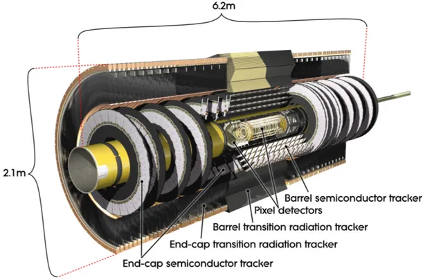
Figure 1.4: Representation of the ATLAS Inner Detector with the SCT and TRT tech-nologies disposition in the barrels and end-caps; inside the barrels it is arranged the Pixel Detector.
Inner detector The Inner Detector (ID) is contained within a cylinder of length 7 m and a radius of 1.15 m, surrounded by the solenoidal magnetic field of 2 T [2]. Pat-tern recognition, momentum and vertex measurements, and electron identification are achieved with a combination of discrete high-resolution semiconductor pixel and strip detectors in the inner part of the tracking volume, and continuous straw-tube track-ing detectors with transition radiation capability in its outer part. The momentum and vertex resolution targets require high-precision measurements to be made with fine-granularity sub-detectors, presented below, arranged on concentric cylinders around the beam axis in the region with |η| < 1, while the end-cap detectors are mounted on disks perpendicular to the beam axis.
Figure 1.5: Detailed illustration of the effective dimensions of the ID tracking system around the beam pipe.
TRT The Transition Radiation Tracker (TRT) is based on the use of straw tubes of 4 mm in diameter, giving a fast response and good mechanical properties for a maxi-mum straw length of 150 cm. This sub-detector can operate at the very high rates and electron identification capability is achieved added by employing Xenon gas to detect transition-radiation photons created in a radiator between the straws. This technique, which is intrinsically radiation hard, allows a large number of measurements on every track. However the detector has to cope with a large occupancy and high counting rates. The structure of the barrel consists of about 50000 straws, each divided in two at the centre in order to reduce the occupancy and read out at each end. The end-caps contain 320000 radial straws, with the readout at the outer radius giving a total number of elec-tronic channels of 420000. Each channel provides a drift-time measurement, resulting in a spatial resolution of 170 µm per straw. These allow the detector to discriminate between tracking hits and transition-radiation hits.
Two end-caps, each consisting of 18 wheels, cover the radial range from 48 to 103 cm. The TRT contributes to the accuracy of the momentum measurement in the Inner De-tector by providing a set of measurements roughly equivalent to a single point of 50 µm precision. It also helps the pattern recognition by the addition of around 36 hits per track, and allows a simple and fast level-2 track trigger.
1.1 LHC and ATLAS state of art 9
SCT The Semiconductor Tracker (SCT) barrel, designed to provide four precision measurements per track in the intermediate radial range, uses four layers of silicon mi-crostrip detectors to provide precision points in the Rφ and z coordinates contributing to the measurement of momentum, impact parameter and vertex position. It also provides good pattern recognition by the use of high granularity.
Each silicon detector is 6.36 × 6.40 cm2 with 768 readout strips each with 80 µm pitch.
The spatial resolution is 16 µm in Rφ and 580 µm in z, and tracks can be distinguished if separated by more than ∼ 200 µm. The system requires a very high dimensional sta-bility, cold operation of the detectors, and the evacuation of the heat generated by the electronics and leakage current.
The readout chain consists of a front-end amplifier and discriminator, followed by a bi-nary pipeline which stores the hits above threshold until the first level trigger decision.
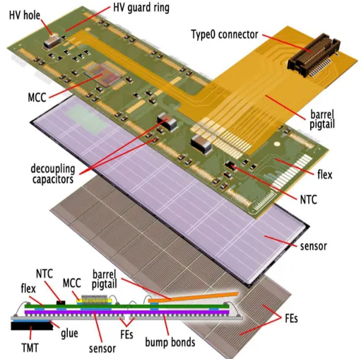
Figure 1.6: Composition of the Pixel Detector, the main tracking system inside ATLAS used to reconstruct interaction vertices.
PD The Pixel Detector (PD) consists of three barrels at average radii of ∼4 cm, 11 cm, and 14 cm, and four disks on each side, between radii of 11 and 20 cm designed to provide a very high-granularity, high-precision set of measurements as close to the interaction point as possible, supplying precision measurements over the full acceptance. It also determines the impact parameter resolution and detects short-lived particles such as b-quarks and τ-leptons.
Figure 1.7: 3D reconstruction of the layers composing the ASIC chips included in the PD.
The readout chips are of large area, with individual circuits for each pixel element, in-cluding buffering to store the data while awaiting the level-1 trigger decision. In addition, the chips are radiation hardened to withstand over 300 kGy of ionising radiation and over 5 × 10¹⁴ neutrons per cm2 in years of operation. The pixel modules are very similar
in design for the disks and barrels; each barrel module is 62.4 mm long and 22.4 mm wide, with 61440 pixel elements, read out by 16 chips each serving an array of 24 by 160 pixels. The output signals are routed on the sensor surface to a hybrid on top of the chips, and from there to a separate clock and control integrated circuit.
1.1 LHC and ATLAS state of art 11
(a) (b)
Figure 1.8: Each readout component of the PD is mounted on staves displaced around the beam pipe with a precise angle to cover the entire geometry.
IBL The Insertable Barrel Layer (IBL) is a fourth layer added to the ID between a new beam pipe and the current PD to face the following issues [3]:
• irreparable failures of modules in the PD layers due to radiation which could have been partially compensated during reconstruction at the cost of an increased fake rate, deteriorating the impact parameter resolution, directly affecting the b-tagging. The IBL restores the full b-tagging efficiency;
• tracking precision is enhanced with IBL located close to the interaction point, improving the quality of impact parameter reconstruction for tracks, and thereby vertexing and b-tagging performances. As a result, sensitivity for signals in physics channels involving b jets is improved;
• luminosity at least twice than the current one is expected before the High Luminosity-LHC (HL-Luminosity-LHC) is complete. With high luminosity the event pileup is increased, leading to high occupancy that can induce readout inefficiencies. Readout inef-ficiencies, particularly at higher luminosity, would limit the b-tagging efficiency. The presence of event pileup requires redundancy in the measurement of tracks in order to control the fake rate arising from pileup background. The addition of the IBL layer helps to preserve tracking performance in face of luminosity effects. For IBL pixel sensors two concurrent technologies are exploited: the well known planar design, already used in the rest of the Pixel Detector, and 3D sensors. The main struc-tural difference between 3D and planar sensors is that the electrodes penetrates the bulk in form of column instead of being implanted on the surface. With this configuration the depletion is parallel to the wafer surface and since the column can be positioned at a distance smaller than the pixel thickness, the voltage necessary for full depletion is smaller, as well as the pulse rise-time. With a small depletion voltage, also the power dissipation due to current leakage is smaller, and with it also the cooling requirements.
(a) (b)
Figure 1.9: IBL planar (a) and 3D (b) pixels read by Front End chips and connected to the readout chain trough flexible circuits.
A new front-end chip, called FE-I4, was fabricated using a 130 nm CMOS architecture and contains readout circuitry for 26880 pixels arranged in 80 columns by 336 rows. The connection of a sensor and a FE-I4 chip plus a flex hybrid, a double-sided flexible printed circuit that allows connection to external services, constitute a module, the basic building block of the IBL detector. According to the sensor used, there are two types of module: planar modules, where a planar sensor is connected to two FE-I4 chips, and 3D modules, where a 3D sensor is connected to a FE-I4. The support structure, holding together 20 modules, electrical services and a cooling pipe is called stave and the entire IBL detector is composed by 14 staves covering the full azimuthal angle and |η| < 3.
1.2 Phase-II upgrade 13
1.2
Phase-II upgrade
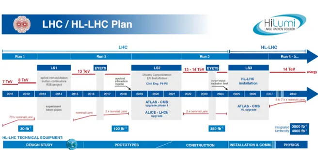
Figure 1.10: Roadmap of LHC main upgrade stages together with centre of mass energy and integrated luminosity targets to be reached.
To sustain and extend its discovery potential, the LHC will undergo a major upgrade in the 2020s. This will increase its instantaneous luminosity (rate of collisions) by a factor of five beyond the original design value (5 × 1034 cm−2s−1) and the integrated
luminosity (total number of collisions) by a factor ten (250 fb−1 per year). This upgrade
will require new infrastructures (underground and on the surface) and over a decade to implement. The new configuration, known as HL-LHC, relies on several key innovations that push accelerator technology beyond its present limits [4]. Among these are cutting-edge 11–12 Tesla superconducting magnets, compact superconducting cavities for beam rotation with ultra-precise phase control, new technology and physical processes for beam collimation and a renewed data acquisition chain.
The present roadmap of LHC, as defined consequently of the corona-virus pandemic, plans by the end of Run 3 main equipment upgrades and layout modifications for ATLAS and CMS, the two high-luminosity general-purpose detectors. The ATLAS and CMS detectors will be upgraded to handle an average pile-up, the number of events per bunch crossing, of at least 140 (ultimately 200) for operation with 25 ns beams consisting of 2760 bunches at 7 TeV, and for an inelastic cross-section σin = 81 mb. These detectors
are also expected to handle a peak line density of pile-up events of at least 1.3 events per mm per bunch crossing and ultimately larger values with limited reduction of the detection efficiency.
HL-LHC The foreseen upgrade should provide the potential for good performance over a wide range of parameters. The machine and experiments will find the best practical set of parameters in actual operation but the most relevant ones for optimizing the luminosity performance can be listed here:
• the total beam current will be a hard limit in the LHC since many systems, like RF power system and RF cavities, collimation system and absorbers, are affected by this parameter. Apart from radiation effects, all existing systems have been designed for Ibeam = 0.86 A; however, the HL-LHC will need to go 30% beyond
ultimate beam current with 25 ns bunch spacing;
• the beam brightness, the ratio of the bunch intensity to its transverse emittance, is a beam characteristic that must be maximized at the beginning of beam generation and preserved throughout the entire injector chain and the operation cycle in the LHC itself. The HL-LHC project has as its primary objective increasing the number of protons per bunch above the nominal design value while keeping emittance at the present low value;
• the beta function, which determines the maximum amplitude a single particle tra-jectory can reach at a given position in the ring, is determined by the focusing properties of the lattice. A classical route for a luminosity upgrade with head-on collisions is to reduce β∗(β at the interaction point) using stronger and larger
aper-ture quadrupoles thus reducing the transverse size of the luminous region resulting in a gain in peak luminosity;
• the luminosity reduction factor R is reduced by a larger crossing angle required to keep a small β∗ and to face this difficulty various methods can be employed to
at least partially mitigate this effect. The most efficient and elegant solution for compensating the geometric reduction factor is the use of special superconducting RF cavities, capable of generating transverse electric fields that rotate each bunch longitudinally.
The expected installation of new equipment, and the previous de-installation and removal of the LHC equipment over a length of about 1.2 km, covers new technologies and infrastructures such as:
• almost complete renewal of the insertion region IR1 (around ATLAS experiment) and IR5 (around CMS), from the quadrupoles to the cryogenics and vacuum sys-tems with the installation of new collimators in IR1 and IR5; as well as the upgrade of most secondary collimators and the insertion of crab cavities;
• installation of one new large 1.9 K refrigerator unit at both P1 and P5 providing the cooling power needed to absorb the five times larger heat load and, with the adoption of a new cryogenic distribution line;
• modification of the extraction and injection systems, in particular installation of new upgraded absorbers to cope with injection failures.
1.2 Phase-II upgrade 15
ATLAS upgrades The upgrade of the central tracking system for the ATLAS exper-iment for the operation at the HL-LHC will start in the middle of 2026. At that time the LHC will have been upgraded to reach a peak instantaneous luminosity of 7.5 × 1034cm−2s−1, which corresponds to an average of about 200 inelastic proton-proton
col-lisions per beam-crossing. The new tracking detector will be operational for more than ten years, during this time ATLAS aims to accumulate a total data set with integrated luminosity of 4000 fb−1.
Meeting all of the requirements of a charged particle tracking detector, close to the beam-line at the HL-LHC, presents a unique challenge for the design of an all-silicon system. In any case, its design can benefit from the enormous amount of experience gained over more than two decades in the construction and operation of the existing inner tracking detector, that has been highly successful for the exploitation of LHC physics up to and well beyond its original design requirements.
Figure 1.11: Display of the ATLAS Phase-II Inner Tracker ITk layout with all its shells.
ITK The development of the new Inner Tracker (ITk) detector layout is carried considering the following set of goals [5]
• designing a tracking detector that provides the required tracking performance to the ATLAS Phase-II physics programme, in events with an average pile-up of up to 200 simultaneous interactions;
• the detector should provide robust tracking in presence of detector defects, like sensor inefficiencies due to expected radiation effects, as well as dead modules due to eventual component failures;
• the aim to minimise cost by reducing as much as possible the total silicon surface necessary to achieve the required hit coverage and by choosing simple solutions whenever possible;
• try to choose layout options that allow minimising the CPU time needed for recon-struction, which is one of the cost drivers for the computing budget for the ATLAS Phase-II programme.
Figure 1.12: Schematic layout of one quadrant of the ITk Inclined Duals layout for the HL-LHC, the active elements of the barrel and end-cap Strip Detector are shown in blue, for the Pixel Detector the sensors are shown in red for the barrel layers and in dark red for the end-cap rings.
The layout of ITk combines precision central tracking in the presence of pile-up events with the ability to extend the tracking coverage to a pseudorapidity of 4 while maintaining excellent tracking efficiency and performance. The ITk comprises two subsystems: a Strip Detector, that has four barrel layers and six end-cap petal-design disks covering |η| < 2.7, surrounding a 5 layers Pixel Detector that extends the coverage to |η| < 4.
1.2 Phase-II upgrade 17
Even though ITk is still in R&D phase, the requirement to be able to replace the inner section of the ITk Pixel Detector during a long LHC shutdown places severe constraints on the design of the pixel package. The mechanical design is thought not to rely on the presence of the inner section. Besides, the pixel package must be able to support the beam pipe without requiring the inner section to be present, in the same way the IBL was implemented in 2014 around a new, smaller radius beam-pipe. In this way, it is possible to guarantee the integrity of the ATLAS detector and some limited data taking capabilities even in event of catastrophic failures of the inner section, such failures that could be repaired in a long shutdown.
The new pixel module will be a hybrid pixel module similar to the one adopted for the present ATLAS Pixel Detector and the IBL. The hybrid pixel module is made of two parts: a passive high resistivity silicon sensor and a front-end read-out chip fabricated in CMOS technology, called a bare module, and a flexible PCB, called a module flex. The silicon sensor and front-end read-out chip are joined using a high-density connection technique. There will be three types of hybrid pixel modules:
• quad modules consisting of four chips bump-bonded to a single sensor, (around 4 × 4 cm2 in area), which are used in the outer flat barrel layers and the outer end-cap
rings;
• dual modules consisting of two front-end chips bump-bonded to a single sensor, (around 4 × 4 cm2 in area), which will be used in the innermost barrel layer and
the inclined part of the outer barrel;
• single-chip modules consisting of one front-end chip bump-bonded to a sensor (around 2 × 2 cm2 in area) required for the inclined part of the innermost barrel
layer.
Compared to the design used for the IBL, the ITk Pixel module required several im-provements:
• the pixel size has been reduced to 50 × 50 µm2 or 25 × 100 µm2to improve intrinsic
resolution and two-track separation;
• the design of the read-out chip has been improved in several ways: the analogue front-end can operate at lower threshold compensating for the loss of collected charge due to radiation damage, the read-out architecture has been improved to comply with the higher hit density and event rate and the radiation tolerance has been increased to 1.4 × 10¹⁶n
eq/cm2. The power consumption was also reduced and
this has a positive effect on the material budget (less massive cables and reduced cooling requirements);
• the output bandwidth has been increased to 5.12 Gb/s per front-end chip, to cope with the hit rates in the innermost section of the tracker;
• the size of the module has been increased; with the largest module the size of four front-end chips, which is about 16 cm2, to reduce cost and fabrication time.
TDAQ Meeting HL-LHC requirements poses significant challenges to the Trigger and to the Data Acquisition system (TDAQ) to fully exploit the physics potential of the new collider. The overall goal of the TDAQ Phase-II upgrade project is to design, build, and install new trigger and data acquisition hardware with its firmware and needed software during the third long shutdown of the LHC in 2024 [6]. A baseline architecture, based on a single-level hardware trigger with a maximum rate of 1 MHz and 10 µs latency has been proposed and, compared to the existing ATLAS Detector, the design of the TDAQ system for the ITk Pixel Detector is much more challenging. This is due to the larger trigger rate (10 times higher than current ATLAS), the larger number of hits associated with 200 proton-proton interactions per crossing and associated volume of data that is generated, in particular in the inner layers.
Figure 1.13: Schematic of the overall baseline design of the TDAQ system in Phase-II with the trigger levels and dataflow indicated in the legend aside. In particular the DAQ system is made up of FELIX, the Data Handlers, and the Dataflow subsystem at 1 MHz.
1.2 Phase-II upgrade 19
In details, the new set-up expects the Inner Tracker, the Calorimeters and the Muon System to produce the first level L0 of trigger data at 40 MHz, and this will be handled by a series of event filters and trigger logic from L0Calo and L0Muon. Once a Global Trigger has been processed and gone through the Central Trigger Processor (CTP), the L0 accept signal will be received by the FELIX board. The FELIX will also receive the read-out data from detectors at 1 MHz and, once all these informations have been collected, the Dataflow will proced with the Event Builder, the Storage Handler and the Event Aggregator, ultimately providing data both to the Permanent Storage and the final Event Filter where data are processed in farms.
Therefore, the FELIX will play a pivotal role in receiving the trigger and the data as a unique, versatile and programmable board and this thesis focuses on its development and functioning test.
The older generation of data links that operate at 160 Mb/s will be replaced with a new design that provides multi-Gb/s read-out without increasing the mass inside the tracking volume, taking advantage of increased performance available in modern electronics. Each front-end chip will have four serial output lines that can transmit data at 1.28 Gb/s (for a total of 5.12 Gb/s). This serial outputs will be coupled to an electrical data transmission line, connecting the front-end chip with the optical conversion stage.
ATLAS aims to fully explore the mechanism of electroweak symmetry breaking through the properties of the Higgs boson, to search for new physics through the study of rare Standard Model processes, to search for new heavy states, and measure the properties of any newly discovered particles. Both the necessity of a highly efficient selection of events with Higgs bosons in decay modes and of events accessing new, unexplored physics scenarios requires exceptional trigger and data acquisition performance.
The new TDAQ will benefit from increased granularity provided by the calorimeters, improved efficiency for muon-based triggers and will perform hardware-based tracking profiting from the extended coverage of the ITk. This is why the upgrade of the TDAQ system will require larger bandwidth and a better processing capacity than the actual one to efficiently select events at high luminosity.
In detail, the expected ATLAS physics programme for the HL-LHC will cover a wide spectrum of physics goals and a representation of analyses including:
• unveiling the paradigm of electroweak symmetry breaking through precision mea-surements of the properties of the Higgs boson;
• improved measurements of all relevant Standard Model parameters including the study of rare Standard Model processes;
• searches for Beyond the Standard Model (BSM) signatures and flavour physics; • specific challenges of the heavy-ion physics.
The new architecture of the TDAQ system will rely on a single-level hardware trigger ( Level-0, formed using calorimeter and muon information) with a detector readout rate of 1 MHz and a maximum latency of 10 µs. The Phase-I calorimeter trigger processors
will be maintained during the HL-LHC operations, and their firmware optimised for the pile-up conditions also complementing it by additional processors that will implement more sophisticate algorithms to provide additional background rejection.
The Event Filter (EF) system will select events based on a processor farm and a custom Hardware-based Tracking for the Trigger (HTT) to reduce the overall CPU require-ments. Each system and sub-system is designed to be capable of evolving to a dual-level hardware-based trigger architecture as a mitigation strategy in case pile-up conditions at the HL-LHC either challenge the readout capabilities of certain detectors (for example of the innermost layers of the ITk) to the limits of the bandwidth available or in case the rates of hadronic trigger signatures surpass the current predictions.
The result of the Level-0 trigger decision is transmitted to all detectors, upon which the resulting TDAQ data are transmitted at 1 MHz through the Readout subsystem, which contains the Front-End LInk eXchange (FELIX) and Data Handler components, and the Dataflow subsystem, which contains the Event Builder, Storage Handler, and Event Aggregator components. Together these compose the DAQ system.
1.3 FELIX project 21
1.3
FELIX project
The Front-End LInk eXchange (FELIX) is a new detector readout component being developed by Brookhaven National Laboratory (BNL) as part of the ATLAS upgrade effort and it is designed to act as a data router, receiving packets from detector front-end electronics and sending them to programmable peers on a commodity high bandwidth network.
FELIX will be the main interface between the detector and all off-detector systems and his main task is to handle the communication between the off-detector back-end systems and the detector.
Whereas previous detector readout implementations relied on diverse custom hardware platforms, the idea behind FELIX is to unify all readout across one well supported and flexible platform, implementing detector data processing in software hosted by commod-ity server systems subscribed to FELIX data.
A first version of the FELIX board, the FLX-712, has been produced and tested to be implemented in the TDAQ upgrade of Phase-I of ATLAS, in particular the LAr Phase-I upgrade of the Trigger readout (both off- and on-detector) and the New Muon Small Wheel readout. The PCB employs two main I/O technologies: high speed optical fibres (up to 768 Gb/s) and the PCIe connection (up to 120 Gb/s) to control and configure the Front End (FE) chips and acquire data from calibration and detection procedures.
Figure 1.14: FLX-712 hosting a Xilinx Kintex Ultrascale FPGA (circled in red), a PCIe Gen.3 X16 connector (circled in orange), the MiniPODs (circled in light blue) and the connector for a Timing and Trigger Control (TCC) mezzanine.
Figure 1.15: Block diagram of the FLX-712 main transmission lines. There are present 8 (4 for the Transmitter and 4 for the Receiver) electro-optical MiniPOD transceivers handled by the GTH protocol of the FPGA, a PCIe connection at 16 lanes (8 transmitting and 8 receiving), a Micro controller to manage the JTAG, the SMBus, the trigger FPGA programming and a flash memory, and Jitter cleaner to provide a very stable clock to the board.
Since the board is thought to be easily programmable and reconfigurable, its com-mercial connections both electrical and optical and the versatility of the FPGA are its main stroing points.
From a network perspective, FELIX is designed to be flexible enough to support multiple technologies, including Ethernet and Infiniband. Given the general purpose nature of the FELIX effort, the system will also be adopted by other non-ATLAS projects. Data, as processed by the FELIX system, are distributed via commodity multi-gigabit networks with at least 100 Gb/s network links that will be used throughout the DAQ system. FELIX supports two different link protocols for the transfer of data to and from front-end peers, each supported by the same hardware platform, with separate firmware revisions both based on the same core modules:
• the Gigabit Transceiver (GBT) chipset and associated technologies, developed as part of CERN’s Radiation Hard Optical Link Project, whose goal is to achieve a radiation hard bi-directional link for use in LHC upgrade projects. GBT provides as interface an optical connectivity technology known as the Versatile link which provides high bandwidth and radiation hard transport of data up to 5 Gb/s; • the FULL mode protocol (referring to full bandwidth) is implemented as a single
wide data stream with no handshaking or logical substructure, given the require-ment for a higher bandwidth data link, from the detector to FELIX, than GBT.
1.3 FELIX project 23
Seeing as not required radiation hardness, the FULL mode protocol can be imple-mented in FPGAs on both sides of the link.
The reduced constraints mean that FULL mode links can operate at a line trans-mission rate of 9.6 Gb/s which, accounting for 8b10b encoding, means a maximum user payload of 7.68 Gb/s.
(a) (b)
(c)
Figure 1.16: Progressive substitution during Phase-I upgrade of the present readout system, based on custom boards, with the FELIX project board, which will be faster and more versatile.
FELIX Phase-II
At the present state of the FELIX project, the 24 layers board hosts an FPGA from Xilinx with 16 nm technology, a PCIe connector to interface with the readout system and a FPGA Mezzanine Connector (FMC) to link to the ATLAS Timing, Trigger and Control (TTC). Several electro-optical transceivers are organized on the board providing large bandwidth to transfer data at higher rates with respect to the DAQ system in use. Here follows a representation of the board with detailed description of its main components.
(a)
(b)
Figure 1.17: Top view of the FELIX Phase-II board with its main components high-lighted in blue. 1) Xilinx Virtex Ultrascale+XCVU9P-FLGC2104AAZ FPGA, 2) DDR4
slot (on top of the FPGA in (b)), 3) 12-channels 25G Duplex Finisar Board-mounted Op-tical Assembly (BOA), 4) 12-channels 25G Duplex Amphenol ICC On-Board Trnsceiver (OBT), 5) 12-channels 16 Tx/Rx Samtec FireFlyT M, 6) 4-channels 25G Duplex Samtec
FireFlyT M. On the back of the board there is also the FMC connector. The PCIe
con-nector (below the FPGA) is a PCIe Gen.3 X16 concon-nector with a nominal data-rate of 15.754 GB/s.
1.3 FELIX project 25
Since the firmware of the FPGA is still under development it is not possible to produce a block diagram as it has been done for the FLX-712 board, which is a previous version. Although it can still be presented a recap of the main interfaces and connection of FELIX Phase-II board.
Figure 1.18: Summary representation of the variety of the connections managed by the FPGA on the FELIX Phase-II board, these are divided into memories (Flash and DDR4), clock distribution, power management and monitoring components and, above all, a wide spectrum of data lines with different number of channels and data-rate.
The main idea behind the FELIX concept is the development of a modular system which makes it possible to independently upgrade or modify aspects of the system such as computing and buffering resources, network technology or supported serial-link protocols. The ability to evolve through further upgrades is a key feature of the readout system when considering the performance requirements and long development cycle leading to Phase-II, as well as the long lifetime of the ATLAS experiment beyond this period. Part of the process leading to the development of such a board is the validation of its channels and transmission lines, in order to ensure integrity in the data transmission. The following section is devoted to highlighting the importance of simulating the functioning of signal transmission lines when dealing with data-rates of the order of GB/s, as in the case of the FELIX board.
Later on, it will be presented the study of two of the channels of data transmission: the 4-channels 25 Gb/s Transmitters (Tx) and Receivers (Rx), and the 16-lane 8 Gb/s PCIe connection. I have chosen these two transmission lines since the former is one of the fastest electro-optical connection, and the latter because its topology is one of the most complicated on the PCB and this could cause problems at such high data-rates.
Chapter 2
Signal Integrity
Until 30 years ago most people treated Printed Circuit Boards (PCB) as totally pas-sive devices for connecting components together. As long as the traces were connected to the correct pins, boards almost never had a negative impact on circuit performance. Traditionally, digital design was a relatively uncomplicated affair. Designers could de-velop circuitry operating up to 30 MHz without having to worry about issues associated with transmission line effects because, at lower frequency, the signals remained within data characterization, allowing the system to perform normally.
In recent decades this is becoming less and less true as we reached frequencies of the order of GHz. Many board designers now need to worry about the parasitic elements of traces (resistance, capacitance and inductance), the interaction between individual traces, and even the interaction between traces and the outside environment. In the present era, where clock frequencies are increased and signal integrity problems are get-ting more severe, product design teams have one chance to get a product to the market; the product must work successfully the first time. If identifying and eliminating signal integrity problems is not an active priority as early in the product cycle as possible, chances are the product will not work.
This is true also for PCBs developed in High Energy Physics (HEP) experiments like the FELIX board, and this is the reason why this new board deserves to be investigated in the light of Signal Integrity (SI).
High-speed digital design, in contrast to digital design at low speeds, emphasizes the behaviour of passive circuit elements. These passive elements may include the wires, circuit boards, and integrated circuit packages that make up a digital product. At low speeds, passive circuit elements are just part of a product’s packaging while at higher speeds they directly affect electrical performance. High-speed digital design studies how passive circuit elements affect signal propagation (ringing and reflections), interaction between signals (crosstalk), and interactions with the natural world (electromagnetic interference).
2.1
Signal Integrity
The term SI addresses two concerns in the electrical design aspects: the timing and the quality of the signal [7][8]. Whether the signal reaches its destination when it is supposed to, and if it is in good condition when it gets there are the most recurring questions. The goal of signal integrity analysis is to ensure reliable high speed data transmission. The quality of the signal needs to be maintained for the receiver in an electronic design to deliver its intended goal.
The failures in high-speed digital circuit are often not readily reproducible. They are often difficult to diagnose, reproduce and fix; unlike the errors in the schematics and layout stage, where, it is possible to check the design using simple rules and instruments. High-speed design failures show up as failures at higher operating frequency, data error rates, cross talk errors and EMI errors. The debugging of high speed related errors may need expensive instruments, for example high bandwidth oscilloscopes, spectrum analysers, time domain reflectometers, to detect and understand the failure mechanism. Therefore, care must be taken at the design stage itself to ensure that the design is in accordance to high speed design rules.
Modern day examples of the high-speed signals include DDR Bus, HyperTransport Bus, USB, SATA, PCIe, Gigabit Ethernet, optic fibre transmission etc. High-speed design techniques must therefore be applied to the PCBs like FELIX containing mentioned and other high-speed signals to ensure proper and reliable operation.
2.1.1
Transmission
In a digital system, a signal is transmitted from one component to another in the form of logic 1 or 0, which is actually at certain reference voltage levels. At the input gate of a receiver, voltage above the reference value Vih is considered as logic high, while voltage
below the reference value Vil is considered as logic low. The ideal voltage waveform in
the logic world would be a square waveform whereas in fact the signal often looks more like a rising wave with noise and oscillations around reference values. More complex data, composed of a string of bits 1 and 0, are actually continuous voltage waveforms and the receiving component needs to sample the waveform in order to obtain the binary encoded information. The data sampling process is usually triggered by the rising edge or the falling edge of a clock signal thus the data must arrive at the receiving gate on time and settle down to a non-ambiguous logic state when the receiving component starts to latch in. Any delay of the data or distortion of the data waveform will result in a failure of the data transmission.
2.1 Signal Integrity 29
2.1.2
Main issues
SI refers to a broader sense to all the problems that arise in high-speed products due to the interconnects. It is about how the electrical properties of the interconnects, inter-acting with the digital signal’s voltage and current waveforms, can affect performance. All of these problems basically can be grouped in three categories: timing, noise and Electromagnetic Interference (EMI).
Timing Timing, which is a complicated field of study, is everything in a high-speed system. Signal timing depends on the delay caused by the physical length that the signal has to cover. It also depends on the shape of the waveform, that can be distorted, when the threshold is reached. In one cycle of a clock, a certain number of operations have to happen: this short amount of time must be divided up and allocated to various operations. For example, some time is allocated for gate switching, for propagating signal to the output gate, for waiting for the clock to get to the next gate and for waiting for the gate to read the data at the input. Thus timing plays a crucial role in every high-speed PCB.
Noise There are several SI noise problem such as ringing, ground bounce, reflections, near-end crosstalk, switching noise, non-monotonicity, power bounce, attenuation etc. All of these relate to the electrical properties of the interconnects and how the electrical properties affect the waveform of the digital signals. Here are explained in more detail some of the most encountered noise problems:
• ringing is an unwanted oscillation, particularly in the step response (the response to a sudden change in input) of a voltage or current. It happens when an electrical pulse causes the parasitic capacitances and inductances in the circuit (those that are not part of the design, but due to the materials used to construct the circuit) to resonate at their characteristic frequency.
Ringing, which can be due to signal reflection, is undesirable because it causes extra current to flow, thereby wasting energy and causing extra heating of the components. It can also cause unwanted electromagnetic radiation to be emitted, it can delay arrival at a desired final state and it may cause unwanted triggering of bistable elements in digital circuits;
• reflection occurs when part of a signal transmitted along a transmission medium, such as a copper cable or an optical fibre is reflected back. This happens because imperfections in the cable cause impedance mismatches and non-linear changes in the cable characteristics that can cause some of the transmitted signal to be reflected.
Impedance discontinuities cause attenuation, distortion, standing waves, ringing and other effects because a portion of a transmitted signal will be reflected back to the transmitting device rather than continuing to the receiver, much like an echo.
This effect is compounded if multiple discontinuities cause additional portions of the remaining signal to be reflected back to the transmitter.
When a returning reflection encounters another discontinuity, some of the signal rebounds in the original signal direction, creating multiple echo effects. These forward echoes strike the receiver at different intervals making it difficult for the receiver to accurately detect data values on the signal;
• crosstalk is any phenomenon by which a signal transmitted on one circuit or channel of a transmission system, like a simple copper line, creates an undesired effect in another circuit or channel. It is usually caused by undesired capacitive, inductive, or conductive coupling from one circuit or channel to another which is close to the transmitting line. This effect is closely related to the distance among to lines since every electrical signal is associated with a varying field, whether electrical or magnetic. Where these fields overlap, they interfere with each other’s signals and this electromagnetic interference creates crosstalk.
For example, if two wires next to each other carry different signals, the currents flowing in them will create magnetic fields that will induce a smaller signal in the neighbouring wire.
All of the effects listed above are related to one of the this four families of noise sources. Signal quality A net can be thought in its simplest form as a series of metal wires connecting chips together, including not only the signal path but also the return path for the signal current. Signal quality on a single net depends as much on the physical features of the signal trace as on the return path. When the signal leaves the output driver, the voltage and the current, which make up the signal, see the interconnect as an electrical impedance. As the signal propagates down the net what is important is the instantaneous impedance it meets, because this can reflect and distort the signal. For example some features that would change the impedance include: changings in the line width, changings in the layer routed trough a via and the presence of a connector or branches in the paths.
The impact on a signal from any discontinuity depends on the rise time of the signal; as the rise time gets shorter, the magnitude of the distortion will increase. The higher the frequency and the shorter the rise time, the more important is is to keep the impedance the signal sees constant.
Another aspect of SI associated with a single net is related to the timing difference between two or more signal paths, which is called skew. For example when a signal and a clock line have a skew different than expected, false triggering and errors can result. Moreover, if there is a skew between two lines that make up a differential pair (as those present in several data transmission lines on FELIX), some of the differential signal will be converted into common signal and the differential signal will be distorted.
2.1 Signal Integrity 31
Crosstalk As mentioned before, when one net carries a signal, some of this voltage and current can pass over to an adjacent net; even though the signal quality on the first net is perfect, some of the signal can couple over and appear as unwanted noise on the second net. Crosstalk occurs in two different environments: when the interconnects are uniform transmission lines, as in most traces in a circuit board, and when they are not uniform transmission lines, as in connectors and packages. In controlled impedance transmission lines where the traces have a wide uniform return path, the relative amount of capacitive coupling and inductive coupling is comparable. In this case, these two effects combine in different ways at the ends of the quiet line.
Rail collapse Noise can affect not only signal paths, but also the power and ground distribution network that power each chip. When current through the power and ground paths changes, as when a chip switches its outputs or gates switch, there is a voltage drop across the impedance of the power and ground paths. This voltage drop will mean less voltage between the power and ground rails.
In high-performance processors, like the FPGA mounted on FELIX, the trend is to lower power supply voltage, but higher power consumption. This is primarily due to more gates on a chip switching faster. In each cycle, a certain amount of energy is consumed: when a chip switches faster, the same energy is consumed in each cycle but consumed more often, leading to higher performance than average consumption. These factors combine to mean higher currents are switching in shorter amounts of time, and the amount of noise that can be tolerated decreases. As the drive voltages decreases and the current level increase, any voltage drop associated with rail collapse become a bigger and bigger problem.
EMI EMI, also called Radio Frequency Interference (RFI) when in the radio fre-quency spectrum, is a disturbance generated by an external source that affects an elec-trical circuit by electromagnetic induction, electrostatic coupling, or conduction. The disturbance may degrade the performance of the circuit or even stop it from functioning. With clock frequencies in the hundreds of MHz range, the first few harmonics are within the common communication bands of TV, FM radio, cellphone and communication de-vices. This means there is the concrete possibility of electronic products interfering with communications unless their electromagnetic emissions are kept below acceptable lev-els. These considerations are valid also in experiments with high density of electronic components as those that will be present in HL-LHC. Unfortunately EMI gets worse at higher frequencies, the radiated strength from common currents increases linearly with frequency and from differential currents it increases with the the square of the the frequency, posing a hard challenge to SI.
2.1.3
SI methodology
SI simulations and analysis take place several times when developing a new PCB, usually it is divided into pre-layout analysis and post-layout analysis. The most impor-tant thing one can do to enable success with simulation is to define a repeatable process with milestones. Whether designing and simulating on your own, or as part of a large design team like in big collaborations involving physics experiments, it is important to have a strategy to enable an efficient process. The sooner in the design cycle decisions are taken the better it is, in order to have more options and minimize reworking. Therefore, it is preferred to simulate as early in the design process as possible. An efficient design flow including simulation comprises:
• starting simulating in the concept and schematic phase of the design. This is the phase where one can use simulation to pick technologies, drive strength, termi-nation, define the topology and so on. It is where design constraints based on actual simulation rather than rules-of-thumb can be developed. Doing so will en-sure the design rules to be conservative enough without being overly constraining and enabling fast layout;
• when the layout and design of components is in the placement phase, one should pass design constraints based on simulation results. It is useful also to find ways to automate this process in the design flow;
• taking the board that is being simulated from the schematic editor into the PCB editor several times throughout the design process. One can start simulating from placement, then simulate again after some critical nets are routed and at the end run a final post-route verification simulation. So that problems are found as soon as possible it is suggested not to wait until the board is complete to run post-route verification;
• when failures are found in the simulation, the affected nets have to be extract over the schematic tool where the net characteristics can be changed to find a solution. Once the solution is achieved one can implement the change in the schematic or layout, and then take the design back to the PCB editor again for final verification. This simulation methodology is intended to guide through typical steps of simulation and provide tips and resources along the way. As a solid example of methodology, the following is the work-flow adopted by the Mentor Graphics (now Siemens) HyperLynx PCB analysis and verification tool.
In the first stage, the pre-layout analysis, the first step is to create a new free-form schematic, essentially the representation of the electrical connections with proper symbols and names of the board circuits.
The subsequent stage is to define the stack-up of the project; typically current PCB have several layers (24 in the case of FELIX) of different materials and dimension that specify their impedance and other parameters.
2.1 Signal Integrity 33
Next, the routing constraints, based upon actual stack-up and technologies, are passed to the layout before translating it into a PCB. Once the PCB has been rendered with a proper tool the post-layout analysis can take place. In the very first glance, the stack-up, the power supplies, the crosstalk thresholds and other parameters have to be checked, then net by net, component by component, one assigns a model to each Integrated Circuit (IC).
By assigning a model, often supplied by the part constructor, one specifies the exact model for that specific IC and how it works in a wide range of conditions. Basically the model contains the results from simulations of the response of the component to a series of stimuli.
Once the models of the ICs in the interested net have been chosen, the effective simulation (which is explained in detail in the next chapter) can start.
From the analysis of simulation results one can study all the possible issues treated before, look at their behaviour and see how they are related to the variation of parameters and topology of the nets. In case a net, or a whole part of the PCB, requires to be optimised its scheme is brought back to the free-form schematic editor where it is possible to make crucial changes in order to gain better performances.
Figure 2.1: Schematic work-flow of SI simulation phases as presented in HyperLynx SI: Basic Signal Integrity Methodology resources.
The area of interest of my thesis work has been the post-layout analysis, as the first FELIX Phase-II boards commissioned to Link Engineering had already been produced. In this sense, the simulations which I have produced with final PCB layout could be compared with real on-board tests done with oscilloscopes and physical connection to transmission lines.
Chapter 3
Simulation with HyperLynx
As mentioned in the previous chapter, whenever it comes to realising a high-performance PCB with high-speed digital design, the SI plays a crucial role in driving the decisions. The state of the art of the FELIX project, guided by Brookhaven National Laboratory and ATLAS collaboration at CERN, is the FELIX Phase-II board presented in this thesis and it has been produced by the Link Engineering company of S. Giovanni in Persiceto (BO).
Together with the contribution of the INFN section of Bologna, and the expertise pro-vided by Link Engineering Chief Technical Officer Luca Pelliccioni and the Signal And Power Integrity Analysis Specialist Roberto Carretta, I have performed SI simulations on the FELIX board in the perspective to validate and optimise its functioning.
This is the first time that such considerations and studies of signal quality are carried on over a high-performance board of a wide collaboration like this.
3.1
Groundwork
The SI simulation that I have conducted is part of the post-layout analysis of the project, and the intent of this work is to give a feedback on the reliability of some FELIX transmission lines providing simulation results. In particular the channels of interest that I have chosen to take into account are the PCIe connections (8 Gb/s per lane) and the transmission lines coupled to the optical fibre (25 Gb/s per channel).
These two transmission lines might be affected by some or many of the main issues introduced previously in the second chapter, and therefore it is worth to investigate how they behave in a typical situation of data transfer that can be reproduced with the HyperLynx tools.