Alma Mater Studiorum · Universit`
a di Bologna
Scuola di Scienze
Dipartimento di Fisica e Astronomia Corso di Laurea in Fisica
Organic small molecules semiconductors as
direct X-ray detectors
Relatore:
Prof.ssa Beatrice Fraboni
Correlatore:
Dott.ssa Ilaria Fratelli
Presentata da:
Fabio Raspanti
Abstract
Organic small molecules semiconductors are promising in the field of direct ionizing radiation detection.
Unlike their inorganic counterpart, these molecules are easy to work with, since they are flexible, soluble and can be deposited on electronic devices with very simple processes, such as drop-casting and spin-casting. Moreover, these materials have good detection properties and very low working voltage.
To this day, organic semiconductors have mainly been used in indirect radiation detection, employed both in scintillator and as photodetectors. However, direct detection of ionizing radiation is a far more effective method, since it is performed within a single material and a single conversion, directly from photons to electrical signal; furthermore, it provides a higher signal-to-noise ratio and a faster response time.
In this experimental work, I fabricated four direct detectors based on transistors; two different organic solutions were drop-casted onto the transistors, creating a conduction channel
between source and drain electrodes.
Both these solutions had chlorobenzene as a solvent, with DiF-TES-ADT and DiF-TEG-ADT as solutes, respectively, in a 0.5% concentration.
The purpose of this thesis is dual. Firstly, I want to study how the detectors’ sensitivity is influenced by semiconductor molecules with different Z-number; secondly, I want to test a new drop-casting method (SAC method) and compare it to results previously obtained with traditional deposition methods.
The results are very promising, with very high values of sensitivity obtained with low voltages.
Sommario
I semiconduttori organici a piccola struttura molecolare sono, al giorno d’oggi, molto promettenti nel campo dei rivelatori diretti di radiazioni ionizzanti.
Diversamente dalla loro controparte inorganica, queste molecole sono facilmente utilizzabili in molte applicazioni, grazie alla loro flessibilità, solubilità e alla possibilità di depositarli su componenti elettroniche con processi molto semplici, come il drop-casting e lo spin-casting. Inoltre, questi materiali hanno buone capacità di rivelazione e lavorano con una tensione molto bassa.
Finora, i semiconduttori organici sono stati principalmente utilizzati nella rivelazione indiretta di radiazioni come scintillatori o fotorivelatori. Tuttavia, la rivelazione diretta delle radiazioni ionizzanti è un metodo assai più efficace, perché viene eseguita in un singolo materiale e in un’unica conversione, da fotoni a segnale elettrico. Per questo motivo, fornisce un rapporto segnale-rumore più alto e un tempo di risposta più rapido.
Durante questo esperimento, ho fabbricato quattro rivelatori diretti di radiazioni depositando su dei transistor due diverse soluzioni organiche per drop-casting, creando in questo modo un canale di conduzione fra gli elettrodi di source e drain.
In entrambe le soluzioni è stato usato clorobenzene come solvente, con rispettivamente DiF-TES-ADT e DiF-TEG-ADT come solute in concentrazione 0.5%.
Lo scopo di questo lavoro di tesi è duplice. Il primo obiettivo è studiare come semiconduttori con diverso Z influenzano la sensitivity del rivelatore; il secondo è provare un nuovo metodo di deposizione per drop-casting, chiamato metodo SAC, e confrontarlo con risultati ottenuti in precedenza con metodi di deposizione tradizionali.
I risultati sono molto promettenti, con valori di sensitivity molto elevati ottenuti con un potenziale relativamente basso.
1
Contents
1. Introduction 3
2. Organic Semiconductors as Radiation Detectors – State of the Art 5
2.1 Radiation sources 5
2.1.1 Radioactivity 5
2.1.2 Sources of radiation 6
2.1.3 Photons 7
2.1.4 Sources of photons – X-ray machines 8
2.2 Organic materials 11
2.2.1 Properties 11
2.2.2 Organic compounds 11
2.3 Organic semiconductors 13
2.3.1 General properties 14
2.4 Organic Thin-film Transistors 15
2.4.1 Properties and operating principles 15
2.4.2 Design and fabrication 19
2.4.3 Applications 21
2.5 Solid-state Organic Molecules Detectors 21
2.5.1 Semiconductors and recombination 21
2.5.2 Drift of electrons and holes 23
2.5.3 Desired properties 23
2.6 Semiconductors’ Applications in Indirect Detectors 24
2.6.1 Organic scintillators 24
2.6.2 Photodetectors 27
2.7 Damaging Effects of Radiations on Semiconductors 29
3. Materials and Methods 33
3.1 Detectors’ Structure 33
3.2 Sample Fabrication Process 34
3.2.1 Solutions’ composition 34
3.2.2 Solutions’ deposition method 35
3.3 Electrical Characterization 36
3.4 X-ray Characterization 38
3.4.1 X-ray exposure 39
3.4.2 X-ray effects analysis 40
3.4.3 Data analysis parameters 40
4. Results 41
4.1 Samples 41
4.2 Electrical Characterization 41
4.2.1 Samples TES_S1-TES_S2 42
2
4.3 X-ray Characterization 46
4.3.1 Samples TES_S1-TES_S2 46
4.3.2 Samples TEG_S3-TEG_S4 49
4.3.3 Damaging X-ray effects 49
5. Conclusions 51
3
1 - Introduction
The detection of ionizing radiations, such as Gamma rays, X-rays, high-energy electrons and Alfa particles, is a growing research area offering development opportunities in many fields, from particle physics to medical analysis.
High-energy photons, which constitute X and Gamma rays, can be detected in two different ways, directly or indirectly.
In both methods, interactions with high-energy photons cause primary excitations and ionizations, which consists in generating electron-hole pairs; these pairs interact then within the detection material and produce more electron-hole pairs (second excitation).
In indirect detection, the electron-hole pairs transfer their energy to a scintillator; the scintillator then releases this energy by emitting radiation, usually in the visible wavelength range. The radiation is successively collected by a photo-multiplier tube or a photodiode and converted into an electrical signal representing the incident radiation’s intensity.
In direct detection, an electric field is applied to separate excitons (electron-hole pairs); electrons and holes are attracted to the positive and negative electrodes, respectively, and the resulting photocurrent is associated to the radiation beam.
The main advantage of the latter method over the former is the number of conversions needed. In indirect detection, we have first a conversion from X-rays to visible wavelengths, then another conversion from visible light to electrical signal; in direct detection, on the other hand, we only have one step from photons to electrical signal.
Between the two, direct detection of ionizing radiation is a far more effective method, since it is performed within a single material and provides a higher signal-to-noise ratio and a faster response time.
The properties needed for materials involved in the production of the two types of detectors are similar: high radiation stopping power, in order to have maximum absorption of the incident radiation, good material purity to avoid excitons’ trapping and uniformity to reduce radiation scattering.
Organic semiconductors are becoming more and more popular in radiation detection, because of their good detection properties, flexibility and very low working voltage.
To this day, organic semiconductors have mainly been used as scintillators or as photodiodes; in recent years, the research in the field of direct radiation detection made many steps
forward, revealing new application opportunities.
The purpose of this study is to further develop our knowledge about the application of these materials as direct ionizing radiation detectors. In particular, I establish two distinct goals. I study how the detectors’ sensitivity is influenced by semiconductor molecules with different Z-number; I chose a silicon-based molecule (DiF-TES-ADT) and a germanium-based one (DiF-TEG-ADT).
4
Furthermore, different deposition methods for the organic molecules might have different effects on the crystals’ structure, which consequently affect the electrical and X-ray exposure properties; therefore, I also analyse how a new drop-casting technique affects the devices’ sensitivity. I then compare these results with different deposition methods previously executed (regular drop-casting and spin-casting).
To do so, I create two solutions based on two different organic semiconductors; both the solutions are then applied by means of SAC drop-casting onto the transistors.
Successively, the devices are exposed to ionizing radiations of the X-ray wavelength. Exposition is performed in a dynamic way, with alternating exposure and dark periods, and with different dose rates, in order to get an accurate estimate of the devices’ sensitivity. This work is arranged as follows.
In chapter 2, I examine the current state of the art of organic semiconductors as radiation detectors. I first give a general description of radiation sources and properties of photons. Successively, I briefly show the main features of organic semiconductors and how they are employed in radiation detection; I also discuss the damaging phenomena occurring when these materials are exposed to radiation.
In chapter 3, I present the methods and materials used in this study. I go over the detectors’ structure and how they are fabricated; I also describe how electrical and X-ray exposure characterizations are performed.
In chapter 4, I report the obtained results. I first present the electrical characterization results; then, I present the X-ray exposure data and the damaging effects on the detectors.
5
2 – Organic Semiconductors as Radiation Detectors –
State of the Art
The research interest on alternative materials for innovative ionizing radiation detection is rapidly growing. Traditional materials for direct, solid-state detectors such as silicon,
cadmium, zinc, telluride or mercury iodide, suffer from severe limitations in their processing into large-area pixelated detector matrices.
Therefore, a new type of ionizing radiation detectors needs to be designed, ideally combining ease of processing, low power supply and mechanical flexibility.
In fact, several applications require thin, conformable sensor panels, for a large-area determination of the incoming radiation dose and energy distribution.
As such applications are of high commercial interest, intense efforts have been recently devoted to the realization of large-area direct detectors based on inorganic; these materials, however, still share the limits of expensive or complex growth techniques and maintain stiff mechanical properties.
An alternative, promising approach is based on organic materials as active photodetectors. One of the interesting features of organic materials is their easy deposition over large areas by solution-coating, which can be done with inexpensive techniques, such as drop-casting, inkjet printing and solution shearing, potentially onto flexible substrates.
Moreover, the typical density of organic molecules is very similar to that of human tissue, making them very interesting for medical X-ray direct dosimetry. [1]
2.1 Radiation Sources
Radiations can be categorized in different ways, such as ionizing and non-ionizing, particles and waves, hazardous and non-hazardous.
However, none of these categorizations draws solid boundaries between properties of individual particles comprising the radiation; rather they show the bulk behavior of particle beams. For example, it will not be correct to assert that an electron always ionizes atoms with which it interacts by arguing that it belongs to the category of ionizing particles.
All we can say is that if a large number of electrons interacts with a large number of atoms, the predominant mode of interaction will lead to the ionization of atoms.
Based on this argument, it is safe to say that the categorization of radiation found in the literature on these bases should not be considered to represent individual particles. What this really means is that if we have a very large number of a certain kind of particles, there is a high probability that most of them would behave in the manner characteristic of their categorization.
The theoretical foundations of particle interaction is quantum mechanics, which quantifies the variables related to particle motion, such as momentum, energy and position, in probabilistic terms. The observable is not the particle, as it is in classical mechanics, but its probability density.[2]
2.1.1 Radioactivity
6
It was discovered by French scientist Antoine Henri Becquerel in 1896; he found out that uranium emitted something invisible that fogged his photographic plates. The term radioactivity was successively suggested by Marie Curie.
Originally, three types of radiation were discovered: - α-rays (helium nuclei)
- β-rays (electrons) - γ-rays (photons)
Later on it was found that other particles such as neutrons, protons, positrons and neutrinos are also emitted by some decaying nuclei. The underlying mechanisms responsible for emission of different particles are different.
The process of internal conversion can occur to electrons in any electronic orbit. Units of Radioactivity
Since the most natural way to measure activity of a material is to see how many
disintegrations per unit time it is going through, therefore the units of activity are defined in terms of disintegrations per second. For example, 1 Becquerel corresponds to 1 disintegration per second and 1 Curie is equivalent to 3.7×10¹⁰ disintegrations per second.
Curie is a much bigger unit than Becquerel is and is therefore more commonly used. However, for most practical sources used in laboratories, Curie is too big; therefore, its subunits of milli-Curie and micro-Curie are more commonly found in literature. The conversion factor between Curie and Becquerel is given below. [2]
1 Bq = 1 disintegration/sec
1 Ci = 3.7 × 10¹⁰ disintegrations/sec 1 Bq = 2.703 × 10⁻¹¹ Ci
2.1.2 Sources of radiation
Radiation sources can be divided into two categories: natural and man-made. Natural sources
There are three types of natural sources of radiation: cosmic, terrestrial, and internal. - Cosmic Radiation Sources
The outer space is filled with radiation that comes from a variety of sources such as burning (e.g., our Sun) and exploding (e.g., Supernovae) stars.
These bodies produce immense amounts of radiation, some of which reach earth. On top of these localized sources of radiation, there is also a background radiation of low energy photons; it is known as cosmic microwave background radiation since the photon spectrum peaks in the microwave region of the electromagnetic spectrum. Apart from photons, other particles are constantly being produced in outer space. Most of them, however, never reach the earth either due to magnetic deflection or the earth’s upper protective atmosphere.
- Terrestrial Radiation Sources
This type of radiation is present in small quantities all around us and is more or less inescapable. Our surroundings are contaminated with minute quantities of radiation emitting isotopes.
7
The main sources of terrestrial radiation are uranium and its decay products such as thorium, radium, and radon.
- Internal Radiation Sources
Our bodies contain some traces of radioactive elements that expose our tissues to continuous low-level radiation. This internal radiation primarily comes from Potassium-40 and Carbon-40 isotopes; its intensity is however minimal.
Man-made sources
Right after the discovery of radiation and realization of its potentials, scientists started working on developing sources that could be used to produce radiation in controlled
laboratory environments. These sources are made for specific purposes and generally give off one type of radiation. Common examples of such sources are
- medical x-ray machines - airport x-ray scanners - particle accelerators - lasers
Out of all these sources, the ones used in medical diagnostics and therapy expose the public to the most significant amounts of radiation. [2]
2.1.3 Photons
A photon represents one quantum of electromagnetic energy and is treated as a fundamental particle in the Standard Model of particle physics. In this model, the photon is assumed to have no rest mass. When the photon is traveling in a medium, it slows down due to interaction with the medium and acquires an effective mass. In vacuum, however, it is considered to be massless.
8
Photons do not correspond to only visible light. In fact, light spans a very narrow region of their full energy spectrum (Figure 2.1).
Photons are involved in all types of electromagnetic interactions.
There are many ways to produce photons that are not in the visible light region of the spectrum. For example, whenever a charged particle moves (such as a changing current in a wire), it creates electromagnetic waves around it that propagate in space. These waves are considered to be excitations in the underlying electromagnetic field and a quantum of these excitations is called a photon.
The energy carried by a photon can be absorbed in a number of ways by other particles with which it interacts. Furthermore, like other particles, a photon can scatter off from other particles and even experience gravitational pull.
In terms of radiation exposure and biological damage, we are generally concerned with high energy photons, such as γ-rays, X-rays, and ultraviolet rays. Having high energies, these photons can penetrate deeper and cause more damage than the low energy photons such as visible light.
An important property of photons is that they carry momentum even though they have no rest mass. The momentum pγ of a photon with energy E, frequency ν, and wavelength λ is given by: [2]
𝑝
γ=
𝐸 𝑐=
ℎ 𝜈 𝑐=
ℎ 𝜆 (2.1)2.1.4 Sources of photons - X-ray machines
Photons play very important roles not only in physics, but also in engineering, medical diagnostics and treatment.
Since X-rays are high energy photons and can cause considerable damage to tissues, they are produced and employed in controlled laboratory environments. Production of X-rays is a relatively simple process, in which a high-Z target (i.e. an element having large number of protons, such as tungsten or molybdenum) is bombarded by high velocity electrons (Figure 2.2). This results in the production of two types of X-rays: Bremsstrahlung and characteristic X-rays.
9
Figure 2.2 - Sketch of a typical X-ray tube [2]
Bremsstrahlung refers to the radiation emitted by charged particles when they decelerate in a medium (Figure 2.2). In case of x-rays, the high-energy electrons decelerate quickly in the target material and hence emit Bremsstrahlung. The emitted X-ray photons have continuous energy spectrum (Figure 2.4), since there are no quantized energy transitions involved in this process.
The electrons incident on the target may also attain sufficient energies to knock off electrons from the internal atomic shells of the target atoms leaving them in unstable states. To regain atomic stability, the electrons from higher energy levels quickly fill these gaps. Since the energy of these electrons is higher than the energy needed to stay in the new orbits, the excess energy is emitted in the form of X-ray photons (Figure 2.3).
The energy of characteristic X-rays does not depend on the intensity of the incident electron beam, because the emitted photons always have the energy corresponding to the difference between atomic energy levels.
Since different elements may have different atomic energy levels, the energy of the emitted characteristic X-ray photons can be accurately predicted.
10
Figure 2.3 - Physical process of generation of characteristic X-rays and Bremsstrahlung [2]
X-ray tube spectra generally have more than one characteristic X-ray peak, since there are a number of electronic transitions possible following a vacancy created in one of the inner electronic shells. If an electron from the innermost K-shell is knocked-off, the vacancy can be filled by any of the electrons in the outer shells. If an electron from the L-shell jumps in to fill the vacancy, a photon with an energy of Eγ = EL −EK is emitted. A large number of such photons would appear as a prominent peak in the spectrum. Such a peak is generally referred to as Kα peak. Kβ peak is the result of transitions of M-shell electrons to the K-shell giving off photons with an energy of Eγ = EM − EK (Figure 2.3).
In an X-ray tube the target (anode) is kept very close (typically 1-3 cm) to the source of electrons (cathode). A high electric potential between cathode and anode accelerates the electrons to high velocities.
The maximum kinetic energy in electron volts attained by these electrons is equal to the electric potential applied between the two electrodes. [2]
11
Figure 2.4 - A typical X-ray tube spectrum showing Bremsstrahlung continuum and peaks corresponding to characteristic X-rays [2]
2.2 Organic Materials
Organic molecules are bonded groups of organic elements. The range of chemicals studied in organic chemistry include hydrocarbons (compounds containing only carbon and hydrogen), as well as myriad compositions based always on carbon, but also containing other
elements, especially oxygen, nitrogen, sulfur, phosphorus. In the modern era, the range of organic elements includes:
- Group 1 and group 2 organometallic compounds, i.e., involving alkali (e.g., lithium, sodium, and potassium) alkaline earth metals
- Groups 13-18 of the periodic table, including metalloids such as silicon and germanium. [3][4][5]
2.2.1 Properties
Physical properties of organic compounds typically of interest include both quantitative features, such as melting and boiling points, and qualitative features, like solubility. Melting and boiling properties
Organic compounds typically melt and many boil. In contrast, while inorganic materials generally can be melted, many do not boil, tending instead to degrade. In earlier times, the melting point and boiling point provided crucial information on the purity and identity of organic compounds. The melting and boiling points correlate with the polarity of the molecules and their molecular weight. Some organic compounds, especially symmetrical ones, sublime, that is they evaporate without melting. A well-known example of a sublimable organic compound is para-dichlorobenzene, the odiferous constituent of modern mothballs. Organic compounds are usually not very stable at temperatures above 300 °C, although some exceptions exist.
12 Solubility
Neutral organic compounds tend to be hydrophobic, meaning that they are less soluble in water than in organic solvents. Organic compounds tend to dissolve in organic solvents. Solvents can be of various types, such as pure substances like ether or ethyl alcohol, or mixtures, or the range of pure or mixed aromatic solvents such as benzene and its derivatives. Solubility in the different solvents depends upon the solvent type.
Solid-state properties
Various specialized properties of molecular crystals and organic polymers with conjugated systems are of interest depending on applications, e.g. thermo-mechanical and electro-mechanical such as piezoelectricity, electrical conductivity, and electro-optical properties. For historical reasons, such properties are mainly the subjects of the areas of polymer science and materials science. [3][4][5][6][7][8]
2.2.2 Organic compounds
Conjugated cyclic compoundsIn chemistry, a conjugated system is a system of connected p-orbitals with delocalized electrons in molecules which are conventionally represented as having alternating single and multiple bonds, which in general may lower the overall energy of the molecule and increase stability.
Conjugation is the overlap of one p-orbital with another across an intervening σ bond. A conjugated system has a region of overlapping p-orbitals, bridging the interposed single bonds. They allow a delocalization of π electrons across all the adjacent aligned
p-orbitals. The π electrons do not belong to a single bond or atom, but rather to a group of atoms.
The largest conjugated systems are found in graphene, graphite, conductive polymers,
and carbon nanotubes.Cyclic compounds can be partly or completely conjugated. Annulenes, completely conjugated monocyclic hydrocarbons, may be aromatic, non-aromatic or anti-aromatic.
Aromatic compounds
The term aromaticity is used to describe a cyclic, planar molecule with a ring of resonance bonds that exhibits more stability than other geometric or connective
arrangements with the same set of atoms. Aromatic molecules are very stable, and do not break apart easily to react with other substances. Organic compounds that are not aromatic are classified as aliphatic compounds—they might be cyclic, but only aromatic rings have special stability.
Since the most common aromatic compounds are derivatives of benzene, the word “aromatic” occasionally refers informally to this category, and so it was first defined. Conjugated, planar, cyclic compounds are aromatic and exhibit an unusual stability. The classic example, benzene, has a system of six π-electrons, which forms the benzene ring along the planar σ-ring with its 12 electrons (Figure 2.5). σ-bonds constitute the molecule’s structure, while π-bonds determine the material’s electrical properties, since π -electrons are delocalized and they are therefore involved in electrical conduction.
For benzene, there are two equivalent conjugated Lewis structures, so that the true molecular state is a quantum-mechanical combination of the two structures with six equivalent CC
13
bonds, which are intermediate between single and double bonds, and all of equal length and strength.
Figure 2.5 – Benzene’s structure [6]
Acenes
The acenes or polyacenes are a class of organic compounds and polycyclic aromatic hydrocarbons made up of linearly fused benzene rings. The larger representatives have potential interest in optoelectronic applications and are actively researched
in chemistry and electrical engineering. One of the more studied acenes is pentacene, which is often incorporated into organic field-effect transistors and allows to reach high mobility values.[6][7][8][9]
Figure 2.6 – Acenes’ structure [6]
2.3 Organic Semiconductors
Semiconductors are crystalline solids in which atoms are held together by covalent bonds. Their name comes from the fact that their electrical conduction properties lie between those of insulators and conductors.
14
Organic semiconductors are solids whose building blocks are π
-bondedmolecules or polymers made up by carbon and hydrogen atoms and – at times – heteroatoms such as nitrogen, sulphur and oxygen.
They exist in form of molecular crystals or amorphous thin films. In general, they
are electrical insulators but become semiconducting when charges are either injected from appropriate electrodes, upon doping or by photoexcitation. [10]
2.3.1 General properties
In molecular crystals, the energetic separation between the top of the valence band and the bottom of the conduction band, which is commonly referred to as band gap, is typically between 2.5 and 4 eV, while in inorganic semiconductors the band gaps are typically 1 to 2 eV (Figure 2.7).
This implies that they are, in fact, insulators rather than semiconductors in the conventional sense. They become semiconducting only when charge carriers are injected from two electrodes or generated via doping. Charge carriers can also be generated in the course of optical excitation. It is important to realize, however, that the primary optical excitations are neutral excitons. Efficient photogeneration can only occur in binary systems due to charge transfer between donor and acceptor.
In organic semiconductors, orbitals close to the Fermi level are known as HOMO (Highest Occupied Molecular Orbital, the highest orbital in the valence band) and LUMO (Lower Unoccupied Molecular Orbital, the lowest conduction band orbital).
Figure 2.7– Electron bands in metals, semiconductors and insulators [11]
Otherwise, neutral excitons decay radiatively to the ground state - thereby emitting photoluminescence – or non-radiatively. The optical absorption edge of organic
semiconductors is typically 1.7 – 3 eV, equivalent to a spectral range from 700 to 400 nm, which corresponds with the visible wavelength spectrum.
Because small molecule, crystalline organic semiconductors can have high charge carrier mobility (over 40 cm2/V·s) and offer versatile processing possibilities, they can be
15
2.4 Organic Thin-film Transistor
Since John Bardeen, William Shockley, and Walter Brattain invented the world's first transistor in 1947, inorganic field-effect transistors (FETs) have dominated the mainstream microelectronics industry. They are the fundamental building blocks for basic analytical circuits, such as amplifiers, as well as the key elements for digital combinational logic circuits, such as adders, shifters, inverters, and arithmetic logic units, and are used to build sequential logic circuits, such as flip-flops. Moreover, transistors are essential to the modern memory devices, integrated circuits, and microprocessors used in personal computers and laptops.
Organic thin film field-effect transistors (OTFTs) are particularly interesting as their fabrication processes are much less complex compared with conventional Si technology, which involves high-temperature and high-vacuum deposition processes and sophisticated photolithographic patterning methods. In general, low-temperature deposition and solution processing can replace the more complicated processes involved in conventional Si
technology. In addition, the mechanical flexibility of organic materials makes them naturally compatible with plastic substrates for lightweight and foldable products.
Although OTFTs are not meant to replace conventional inorganic TFTs – because of the upper limit of their switching speed – they have great potential for a wide variety of applications, especially for new products that rely on their unique characteristics, such as electronic newspapers, inexpensive smart tags for inventory control, and large-area flexible displays.
In this section, I will describe the basic working principle of OTFTs and discuss materials requirements and fabrication methods for building these devices, with the related technical issues and challenges. [12][13]
2.4.1 Properties and operating principles
An OTFT is analogous to its corresponding inorganic device in basic design and function. It is a three-terminal device in which a voltage applied to a gate electrode controls current flow between a source and drain electrode under an imposed bias (Figure 2.8).
The control of source-drain current in FETs via a third terminal has resulted in their widespread use as switches.
16
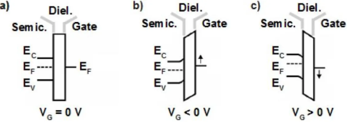
The ideal operation of an n-type OTFT depends on the existence of an electron accumulation layer at the dielectric/semiconductor interface. This ideal operation can be described by analyzing the energy band diagram of the capacitor comprised by the gate electrode, dielectric and semiconductor.
In Figure 2.9, the ideal operation of a n-type TFT is shown: applying a VG <0 V causes a depletion region at the dielectric interface, whileVG >0 V makes a downward band-bending and the appearance of an accumulation region.
In a real device, the two possible regimes of operation are separated by a voltage value, which corresponds to downward band-bending of the semiconductor close to its interface with the dielectric: the threshold voltage (Vth). Vth deviates from 0 V, being a function of the gate electrode-semiconductor work function difference, the background carrier concentration of the semiconductor (N), the charge density residing within the dielectric and the trap density at the interface and within the semiconductor.
Depending on the sign of Vth, two different mode of operation for TFT can be distinguished: enhancement and depletion for positive or negative threshold voltage, respectively (for n-type TFT).
Once defined the threshold voltage, the role of OTFTs as switches is clear.
For VG >Vth, provided that a positive drain voltage (VD) is applied, current flows between the drain and source electrodes (ID), corresponding to the logical high state of the TFT.
For VG <Vth, regardless of the value of VD, the upward band-bending of the semiconductor close to the interface with the dielectric is verified, resulting in a low ID that corresponds to the logical low state.
Figure 2.9- Energy band diagram of an ideal gate electrode/dielectric/n-type semiconductor capacitor for different bias conditions: equilibrium, VG = 0 V (a); depletion, VG <0 V (b);
accumulation, VG >0 V(c) [13]
Considering now the logical high state (or on-state) of the OTFT, depending on the intensity of VD, two different regimes can be distinguished:
1- Pre-pinch off regime VD < (VG - Vth)
In this regime the drain current (ID) can be expressed using the following equation: 𝐼𝐷 = 𝐶𝑖 𝜇𝐹𝐸 𝑊 𝐿 [(𝑉𝐺 − 𝑉𝑡ℎ)𝑉𝐷− 1 2𝑉𝐷 2] (2.2)
where Ci indicates the capacitance of the dielectric per unit area, µFE is the
field effect mobility and W (width),L (length) are the geometrical dimensions of the channel.
17
In this regime, a uniform distribution of charge throughout the entire channel is supposed. When a very little voltage is applied through the drain electrode, the second order term in (2.2) can be ignored and the relation between current and voltage drain becomes linear.
2- Post-pinch off or saturation regime VD > (VG - Vth)
When the drain voltage overcomes (VG - Vth), the accumulation layer close to the drain region becomes depleted, leading to the saturation of ID.
In the saturation regime the drain current can be expressed by: 𝐼𝐷 = 𝐶𝑖 𝜇𝑆𝐴𝑇𝑊
2𝐿[𝑉𝐺− 𝑉𝑡ℎ]
2 (2.3)
where 𝜇𝑆𝐴𝑇 is the saturation mobility.
Equations 2.2 and 2.3are based on some assumptions.
The first one was proposed by Shockley and is known as gradual channel approximation: the gradient of the lateral field within the channel is negligible compared with the variation of the vertical field. This assumption is not valid near the drain electrode or for short-channel devices in the saturation regime.
Another important assumption is the independence of µFE and µSAT from VG.
The electrical performances of OTFTs are described by several parameters evaluable from the electrical characterization of the devices. In Figure 2.10, the transfer and output
characteristic are shown.
Figure 2.10- Transfer (a) and output (b) characteristics of an n-type TFT [13]
From these plots, one can extract several parameters like: On/off ratio
This parameter defines the ratio between the maximum and the minimum value of the drain current. A large value is desirable to obtain a good device for successful usage as electronic switch.
18 Vth / VON
Vth indicates the value to overcome from the gate electrode to achieve an accumulation region in the interface between semiconductor and dielectric layer. This value can be evaluated by a linear extrapolation in the ID-VG plot (for low VD) or in the (ID)1/2- VG one (for high VD). VON indicates the gate voltage value for which the drain current starts to grow, as it is shown in the transfer characteristic in Figure 2.10a.
Subthreshold swing (S)
S is defined as the inverse of the maximum slope of the transfer characteristic. It represents the necessary VG to increase ID by one order of magnitude.
𝑆 = (
𝜕 log (𝐼𝐷) 𝜕 𝑉𝐺)
𝑚𝑎𝑥−1
(2.4)
Mobility µ
Mobility is related to the efficiency of carriers transport in a material and is directly
connected to the maximum ID and to the switching speed of the devices. For instance, it has a direct impact on the maximum operating frequency or cutoff frequency fco, which can be defined as:
𝑓𝑐𝑜 = 𝜇𝑉𝐷
2𝜋𝐿2 (2.5)
The mobility is directly affected by the scattering mechanisms present in the material, for examples by lattice vibrations, ionized impurities, grain boundaries and other structural defects.In the case of TFTs, where the charges have to flow in a narrow region near the dielectric interface, we have to consider other mechanisms of scattering such as Coulomb scattering from dielectric charges and from interface states or surface roughness scattering. As it has already been said, the mobility is modulated by VG and for this reason, depending on the regime, several type of mobility can be calculated:
Effective mobility µeff
Obtained by the conductance (𝑔𝑑 = 𝐼𝐷 𝐿
𝑉𝐺 𝑊 ), with low VD:
𝜇𝑒𝑓𝑓 = 𝑔𝐷
2𝜋𝐿2 (2.6)
This value is difficult to obtain, because it requires the knowledge of Vth. Besides, this is very sensitive to contact resistance because of the low VD.
Field effect mobilityµFE
Obtained with the transconductance (𝑔𝑚 = 𝜕𝐼𝐷
𝜕𝑉𝐺), with low VD:
𝜇𝐹𝐸 = 𝑔𝑚
𝐶𝑖𝑊𝐿𝑉𝐷
19
This value is easier to obtain because, the transconductance is extractable from the transfer characteristic and it does not require the knowledge of Vth. On the other hand, the contact resistance affects this mobility.
Saturation mobility µSAT Obtained with high VD:
𝜇𝑆𝐴𝑇 =( 𝜕√𝐼𝐷 𝜕𝑉𝐺) 2 1 2𝐶𝑖 𝑊 𝐿𝑉𝐷 (2.8)
This mobility does not require Vth and it is less sensitive to the contact resistance, but it describes a situation where the channel is pinched-off and its effective length is smaller than L. [12][13]
2.4.2 Design and fabrication
As previously mentioned, the OTFT inherits its design architecture from its inorganic counterpart, namely the metal-oxide-semiconductor field-effect transistor (MOSFET). It is composed of three main components: source, drain, and gate electrodes, a dielectric layer and the active semiconductor layer. Within the basic MOSFET design, there are two types of device configuration: top contact and bottom contact. The former involves building source and drain electrodes onto a preformed semiconductor layer, whereas the latter is constructed by depositing the organic over the contacts (Figure 2.11). Top contact devices have been reported to have superior performance for certain organic semiconductors compared with their bottom contact counterparts. It has been suggested that this is a result of reduced contact resistance between the electrode and the organic layer because of an increase in the area for charge injection.
20
TFTs are quite similar to other field-effect devices in terms of operation and composing layers, however some important differences exist. While in TFTs the substrate is an insulator, in MOSFETs the silicon wafer plays the role of semiconductor and mechanical substrate at the same time.
Furthermore, fabrication is performed at different temperatures: for MOSFET, a temperature of 1200 K is commonly reached; for TSTs, on the other hand, a lower limit is imposed because of the softening point of the substrate.
MOSFETs have a p-n junction at the source and drain regions, which are absent in the TFTs. Even if both the transistors' operation is based on field effect, MOSFETs work in inversion regime, while TFTs work in the accumulation one.
In a traditional inorganic device, the active semiconductor layer is generally comprised of lightly doped Si, or combinations of Group III-V elements, such as GaAs. In these materials, the applied gate voltage causes an accumulation of minority charge carriers at the dielectric interface, e.g. electrons in a
p
-type material, termed an ‘inversion layer’. In this very shallow channel, carriers injected from the source and drain electrodes may pass, resulting in current flow.In an organic transistor, on the other hand, the active layer is comprised of a thin film of highly conjugated small molecules or polymers.
In stark contrast to inorganic materials, organics pass current by majority carriers, and an inversion regime does not exist. This fundamental difference is related to the nature of charge transport in each of these semiconductors.
In well-ordered inorganics (e.g., single-crystal Si), the delocalization of electrons over equivalent sites leads to a band-type mode of transport, with charge carriers moving through a continuum of energy levels in the solid.
In less-ordered organic materials, the proposed mechanism is hopping between discrete, localized states of individual molecules. The presence of impurities or inconsistencies in structure may result in “traps” that alter the relative energy levels, and inhibit the flow of charge carriers.
The complexities of current flow in organic materials – which are still not fully understood – have added another dimension to the development of the devices that incorporate them. In addition to the challenges presented by fabrication, particular attention must be paid to the design of materials that will meet the performance demands of the OTFT in its parent
applications. This aspect of development has received much attention, and will continue to play an important role as the technologies progress.
The limitations of current organic technologies are clearly posed by the performance and ease of processing of the active layer component. In addition to meeting benchmarks for
performance criteria, such as mobility and on/off ratio, active layer materials should ideally be easy to process, mitigating potential fabrication challenges, and have long-term stability for device longevity. This has proven a difficult balance.
Deposition methods
Deposition of thin film organic semiconductor layers is primarily performed through vapour or solution phase processes. Vacuum deposition is used for small molecules and oligomers. It produces films that show high field-effect mobility and on/off ratios, but it is somewhat costly because of expensive equipment and low deposition throughput.
OTFT device performance can be improved by controlling the deposition rate and temperature, which affect the morphology of the semiconductor. [12][13]
21
2.4.3 Applications
Organics have long been attractive for use in electronics because of their lightweight, flexibility, and low cost compared with their inorganic counterparts. In addition, recent increases in performance have rapidly expanded the range of possible organic FETs applications, making them targets for a wider range of applications.
Organics offer potential advantages in displays, where TFTs are implemented as switches to activate individual pixels.
Hand-held devices with ultrathin displays can achieve higher resolution and information content, while new technologies, such as flexible displays and electronic paper, get closer to being achievable.
In conclusion, the physical properties and relatively easy processing of organic materials allow for the creation of flexible, low-cost, large-area devices using OTFTs. Advances in fabrication methods and the development of higher-performance semiconductor materials have improved on existing technology and expanded the scope of potentially realizable applications. Much of this progress has been a result of the deduction of the relationship between performance and structure of the active layer component.
Molecular tuning based on this understanding has produced materials with better electronic properties and easier processing. While challenges exist for large-scale manufacturing, the rapid development of these materials shows great promise for their future in plastic
electronics. [12][13]
2.5 Solid-state Organic Molecules Detectors
The use of organic materials in ionizing radiation detection is very interesting, thanks to their low cost, flexibility, and simple fabrication compared to the corresponding inorganic
materials.
I know describe how semiconductors behave when they are hit by an incident radiation beam, how they can be used to detect radiation and which properties they should have for this purpose.
I will then mention how semiconductors have mainly been used in detectors to this day, i.e. as scintillators and photodetectors. [1]
2.5.1 Semiconductors and recombination
Radiation passing through a semiconductor material is capable of causing the following three phenomena to occur in the bulk of the material:
1- Lattice excitation: the incident radiation deposits energy to the lattice increasing its vibration.
2- Ionization: the incident radiation causes an electron to gain enough energy to break its bond with an atom; an electron-hole pair is produced’
3- Atomic displacement: this non-ionizing phenomenon is the major contributor to the bulk of the damage caused by radiation.
In semiconductor detectors, the main phenomenon is on the ionization process, but lattice excitations also has a significant impact on the electron-hole pair production.
In a perfect semiconductor material, at a temperature below the band gap energy, all the electrons are in valence band. The conduction band in such a situation is completely empty.
22
The outer shell electrons, taking part in the covalent bonding between lattice atoms, are not free to move around in the material. However, as the temperature raises, some of the electrons could get enough thermal excitation to leave the valence band and jump to the conduction band. This creates an electron deficiency, or a net positive charge, in the valence band and is generally referred to as a hole.
This process can also occur, although at a much higher rate, when radiation passes through the material. If a radiation is capable of delivering energy above a material-specific threshold, it is possible to have the creation of electron-hole pairs in the material.
Figure 2.12 – Electron-hole pair production [11]
This threshold is higher than the band gap energy of material, because some of the energy is expended in increase crystal excitations.
For silicon the threshold is very low (3.62 eV), which makes it highly desirable for use in radiation detectors.
In semiconductors, as in gases, the average energy needed to create an electron hole pair is independent of the type of radiation; it depends exclusively on the semiconductor material and its temperature.
The process of ionization in semiconductors is similar to the ionization in gases, but the energy needed in semiconductors is much lower, between 10% and 25%.
This implies that, the radiation being equal, the number of charge carriers produced in a semiconductor is much higher than in gases.
Because of this property, semiconductor detectors are considered to be superior than gaseous detectors.
The free charges in a semiconductor can drift under the influence of an externally applied field. Just like in metallic conductors, their movement can also be characterized by a
parameter called conductivity, which quantifies the ability of the material to conduct electric current. However, as opposed to metallic conductors, there are some mechanisms that can contribute to or suppress the conductivity of a semiconductor.
An important factor in semiconductor-based detectors is the quality of the crystal lattice. If there were imperfections or impurity in the crystal, energy level in the forbidden gap would be produced, causing a degradation in the production of charge pairs. This would cause imperfections and non-linearities in the detector’s response through an effect called charge “trapping”.
In a trapping process, an electron jumping to an impurity level could be trapped there for some time.
This electron can then do two things: it can either jump up into the conduction band, completing the process of electron-hole pair generation, or fall back into the valence band and recombine with the hole. In the former case, a time delay is introduced in the charge pair production, while in latter no charge pair is produced; the excess energy in this case is not enough to create an electron hole pair, since it will be equal to the energy of the impurity, not to the energy of the gap, and is absorbed by the lattice.
23
Another process that needs to be taken into account is the band-recombination. In this
process, an electron falls from the conduction band into the valence band to recombine with a hole; this form of recombination is the simplest and most prevalent in semiconductors. The result of this process is the removal of the electron from the conduction band and the hole from the valence band. [2]
2.5.2 Drift of electrons and holes
The semiconductor detectors are usually operated in the so-called photoconductive mode; such an operation involves establishment of an electric field across the material.
When the incident radiation produces electron hole pairs along its track in the detector, the charges start moving in opposite directions under the influence of the applied electric field. The velocity with which the charges move depends on the electric field.
For low intensity fields, it has been found that the velocity increases almost linearly with the field strength:
𝑣⃗ = 𝜇 𝐸⃗⃗ (2.9)
where E is the electric field applied and μ is a proportionality constant called mobility. Its value depends on the type of the material.
As the field is further increased, the velocity of the carriers starts showing deviation from the above relation and eventually saturates; most of the detectors are built such that the charges can very quickly attain the saturation velocity, within a few picoseconds.
Based on the drift of electrons and holes, we should now find a proportionality between a measurable quantity and the energy deposited by the incident radiation.
As the charges move in opposite directions, they constitute an electric current with a current density J, which follows Ohm’s law:
𝐽⃗ = 𝜎 𝐸⃗⃗ (2.10)
where σ is the conductivity.
Since current density can also be written as
𝐽⃗ = 𝜌 𝑣⃗ (2.11)
where ρ is the charge density, equations 2.9, 2.10 and 2.11 can be combined to give
𝜎 = 𝜇 𝜌 (2.12)
If now this material is placed in an ionizing radiation field, electron-hole pairs will be created and consequently the number of free charge pairs in the bulk of the material will increase. The result of this will be a change in the conductivity of the material. If n’ represents the number of charge pairs created by the incident radiation, then the change in the conductivity will be given by:
𝛿𝜎 = 𝑒 𝜇 𝑛’ (2.13)
This change in conductivity is proportional to the energy delivered by the incident radiation, provided all other conditions remain constant. Hence measuring the change in conductivity is equivalent to measuring the delivered energy.
Such a measurement can be done by placing the detector in an external circuit, which could measure the change in current caused by change in conductivity.
It should be mentioned here that both electrons and holes take finite amount of time to recombine. Therefore, the output signal actually has a shape with a finite rise and decay times. [2]
2.5.3 Desired properties
The desired properties of semiconductor detectors are highly dependent on the designated application as some of these have conflicting requirements.
24
Semiconductor detectors are highly versatile devices that can be used both in high and low radiation environments, providing that they are built for specifically for that radiation field. For instance, an avalanche photodiode can be used to detect single photons, but would be useless for detecting high intensity radiations, such as gamma rays.
Therefore, we can divide semiconductor detectors in two categories, depending on whether they are used for high or low radiation fields.
For high radiation environments, the most important properties a detector should have are: - Charge collection efficiency: with high incident radiation rates, large numbers of
charge carriers are generated, so a high collection efficiency is required for the electrodes; electron-hole recombination and charge trapping cause deteriorations in charge collection.
- Fast response: the electronics associated with the detector should be fast enough to distinguish between signals that are a few nanoseconds apart.
- Radiation Hardness: the detector should be as resistant to radiation damage as possible.
For low radiation environments, on the other hand, the requirements are different:
- Charge yield: the number of electron-hole pairs created should be enough to provide a good signal to noise ratio.
- Resolution: high energy resolution is essential in low radiation conditions. [2]
2.6 Semiconductors’ Applications in Indirect Detectors
High-energy photons can be detected with two different methods, directly or indirectly. In both methods, interactions with high-energy photons cause primary excitations and ionizations, which consists in generating electron-hole pairs; these pairs interact then within the detection material and produce more electron-hole pairs (second excitation).
In direct detection, an electric field is applied to separate excitons (electron-hole pairs); electrons and holes are attracted to the positive and negative electrodes, respectively, and the resulting photocurrent is associated to the radiation dose absorbed by the detector.
In indirect detection, the electron-hole pairs transfer their energy to a scintillator; the scintillator then releases this energy by emitting radiation, usually in the visible wavelength range. The radiation is successively collected by a photodetector (a photo-multiplier tube or a photodiode) and converted into an electrical signal representing the incident radiation’s intensity.
Indirect detection is less effective, since it causes a lower signal-to-noise ratio and a slower response time. Furthermore, it is performed using multiple devices, resulting in a bulky, inconvenient detector.
To this day, organic semiconductors have mainly been used as scintillators or as photodiodes. In this section, I discuss the main features of scintillators and photodetectors. [14]
2.6.1 Organic scintillators
Organic scintillators are extensively used in radiation detectors. They are found in solid, liquid, and gaseous states. One of the most important advantages of organic scintillators is that they can be produced in virtually any geometry, therefore can be customized to specific applications.
Scintillation Mechanism
The basic scintillation mechanism of organic scintillators is the fluorescence or prompt emission of light following the S-state electronic transitions (Figure 2.13).
25
The incident radiation transfers energy to the atoms causing electronic transitions from S0 ground levels to different vibrational levels in the S1 band; higher band transition are also possible, depending on the energy of the incident radiation.
The induced instability in the system forces the electrons in different S1 vibrational levels to go to the S1 ground level through radiation-less transitions.
These transition are very fast, they are completed within a few tenths of a nanosecond. From there the electrons fall into the S0 ground and vibrational levels with decay times on the order of a few nanoseconds.
The excess energy of the electrons is emitted in the form of fluorescence photons, which for most materials lie in the ultraviolet or visible region of the electromagnetic spectrum.
Figure 2.13 - Typical singlet energy level diagram of organic scintillators [2]
The decay of electrons from the S1 vibrational states to S1 base level is a favorable process especially for scintillation detectors, because during such decays the electrons loose some of their energy.
Consequently, the energy emitted during their transitions from the S1 ground level to the S0 levels is less than the energy absorbed during the radiation-induced transitions from S0 ground level to S1 levels. This essentially implies that the absorption and emission spectra of such materials do not match, hence disfavoring the re-absorption of the scintillation light in the material.
This phenomenon was first observed by Sir George G. Stokes, who later on formulated a principle stating that the wavelength of fluorescence light is always greater than the
wavelength of absorption. This law does not really hold for all wavelengths and all materials since there is always some overlap of emission and absorption spectra.
However, the so-called Stoke’s shift is evident, the emission spectrum’s peak is shifted from the absorption spectrum’s peak.
Stoke’s shift between absorption and emission spectra can be defined as:
∆𝜆𝑆𝑡𝑜𝑘𝑒𝑠 = 𝜆𝑚𝑎𝑥,𝑒− 𝜆𝑚𝑎𝑥,𝑎 (2.14) Where λmax represents the peak of the spectrum with subscripts e and s referring to the
26
A typical emission and absorption spectra of an organic scintillator is represented in Figure 2.14. In general, the higher the Stoke’s shift, the smaller the probability of re-absorption of scintillation light since the overlap area will be smaller.
Figure 2.14 - Typical absorption and emission spectra of an organic scintillator [2]
The above-mentioned transitions is not the sole possible in organic scintillators. Another mode of electron relaxation is through the vibrational levels in the triplet T1 band (Figure 2.15).
As before, the incident radiation transfers the electrons from the S0 ground level to the S1 vibrational levels. These electrons first decay into the S1 ground level through radiation-less transitions. Successively, instead of falling into the S0 level directly, the electrons can first go to the available T1 levels.
These triplet levels are much more stable than the singlet levels and consequently the electrons can be thought of being trapped there for an extended time. From the T1 ground level, into which all electrons eventually decay, they fall into the S0 levels.
This also results in the emission of light, but in this case it is called phosphorescence or delayed fluorescence, since it is emitted after a substantial delay, which is more than 100 ms for typical organic scintillators.
27 Transfer of scintillation photons
Scintillators produce photons of certain wavelengths that normally fall within the visible region of the electromagnetic spectrum.
To detect these photons, photodetectors are used. I will now discuss how the scintillation photons are transferred from the scintillator to the photodetector.
The simplest way to do this is to directly attach a scintillator to a photodetector with greater area, in order to avoid losing photons.
However, the geometries of scintillators and photodetectors normally cannot satisfy these characteristics, with the scintillators usually having areas larger than the photodetectors’. Hence building a detector in such a configuration is generally not possible.
A more practical approach is to use a light guide to connect the photon-emitting surface to the photodetector in such a way that the scintillation photons reach the photodetector with
minimal loss.
A light guide can be constructed in different configurations, but all of them are based on the principle of reflection. [2]
2.6.2 Photodetectors
The photons produced by scintillators can be detected in a number of ways, the most notable of which are photomultiplier tubes (PMTs) and photodiodes (PDs).
Both of these detector types have their own pros and cons. For example, photomultiplier tubes have sensitive mechanical structures that are prone to damage in mechanically unstable environments, while the photodiodes are made of semiconductor materials and are therefore mechanically stable.
On the other hand, the response time of PMTs is much smaller than photodiodes, therefore PMTs are preferred in timing applications.
These are only two of the parameters and the choice of a photodetector is in reality a compromise between many factors, including cost.
Photomultiplier tubes
Photomultiplier tubes are sensitive devices that are capable of converting light photons into a very large number of electrons.
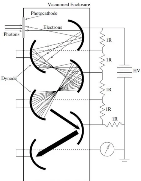
The basic building blocks of a complete PMT are a photocathode, an electron multiplication structure, and a readout electrode.
The photons incident on the photocathode are converted into electrons through photoelectric effect. The electrons are then accelerated and strike a metallic structure called dynode, resulting in the emission of more electrons.
The newly produced electrons are again accelerated towards another dynode, where even more electrons are produced. This process of electron multiplication continues until the electrons reach the last dynode, where an ammeter measures the resulting current (Figure 2.16).
The most important characteristics that make PMT-based photodetectors desirable for radiation detection are:
- High sensitivity
- Good signal-to-noise ratio - Fast time response
28
Figure 2.16 – Working principle of a PMT; in real applications, 10 or more dynodes are used. [2]
With rapidly developing technology, new photodiode are now being able to match or even surpass these properties.
Photodiode Detectors
A photodiode is a semiconductor device that converts light into an electrical current. When photons collide with the device, a current is generated by photoelectric effect. Photodiodes may contain optical filters, built-in lenses, and may have large or small surface areas. They usually have a slower response time as their surface area increases. The traditional solar cell used to generate electric solar power is a large area photodiode.
Photodiodes are similar to regular semiconductor diodes, except that they may be either exposed, to detect UV or X-rays, or packaged with a connection to allow light to reach the sensitive part of the device. Many diodes designed for use specifically as a photodiode use a PIN junction rather than a p–n junction, to increase the speed of response. A photodiode is designed to operate in reverse bias.
The material used to make a photodiode is critical to define its properties, because only photons with sufficient energy to excite electrons across the material's bandgap will
29
produce significant photocurrents. Because of their greater bandgap, silicon-based photodiodes generate less noise than germanium-based photodiodes.
Advantages of photodiodes over photomultipliers include:
- Good linearity of output current as a function of incident light - High signal-to-noise ratio
- Good endurance to mechanical stress - Lower cost
- Light weight and small size - Low operation voltage.
On the other hand, disadvantages compared to photomultipliers include: - Small area
- No internal gain - Low overall sensitivity
- Slow response time. [2][15][16][17][18]
2.7 Damaging Effects of Radiations on Semiconductors
A serious problem with semiconductors is their vulnerability to structural damage caused by radiation. Both instantaneous and integrated doses contribute to the overall damage. Although some of these effects can be compensated by increasing the reverse bias, eventually the bulk of the damage renders the detector material useless.
Therefore, deployment of semiconductor-based detectors in highly hostile radiation environments, such as particle accelerators, needs careful consideration and regular monitoring.
Damage Mechanism and NIEL Scaling
The most damaging defects caused by radiation are the result of atomic displacements that destroy the lattice structure. These defects could be dispersed or clustered around the incident radiation track.
Dispersed atomic displacements cause the so-called point defects.
A cluster of such displacements in close vicinity to each other is called cluster defect. The distinguishing feature of clustered defects is that they make a large region of the bulk of the material useless.
The main damage mechanism is the displacement of an atom from its lattice site by an incident particle; this is called Non Ionizing Energy Loss or NIEL.
As opposed to the ionizing energy loss, NIEL is not proportional to the total energy absorbed in the semiconductor and is highly dependent on the type of radiation and its energy.
It should also be mentioned that the atoms displaced by the incident radiation can cause further damage. However, since these recoil atoms usually have a low energy, this effect is not very pronounced.
Hence, in this case NIEL scaling will be a good approximation of the overall damage.
In the case of high energy neutrons, however, the recoil spectrum is more skewed towards the high energy end and therefore NIEL scaling should be interpreted carefully. Independently from which specific damage mechanism is caused, the end result is the performance deterioration of the detector.
30
Shown below are the most important of these deteriorating effects on the detector performance.
Leakage current
One of the main radiation induced damages is the change in reverse bias current; this phenomenon is caused by the increase or decrease in the number of free charge pairs in the depletion region.
The decrease in leakage current, which is generally observed during initial irradiation, is primarily due to production of charge traps in the forbidden energy gap.
After prolonged irradiation, the leakage current can show significant increase, as the
probability of charge pair production increases by introduction of additional energy levels in the forbidden gap.
It has been found that the damage-induced leakage current depends on the radiation dose rate, the exposed volume of the detector, and its temperature.
The dose rate is the amount of absorbed radiation per mass unit and depends of course on the particle flow, which is simply the integrated radiation intensity.
At a certain temperature, the dependence of change in leakage current Δil on particle flow Φ and volume V can be written as:
∆i𝑙 = α V Φ (2.15)
where α is the so-called damage coefficient and depends on the type of incident particle and its flow.
This equation can also be written in terms of leakage current before irradiation i0 and after irradiation ir:
𝑖𝑟 = 𝑖0+ α V Φ (2.16)
The temperature dependence of ir, on the other hand, can be described by Boltzmann function:
𝑖𝑟(𝑇) ∝ 𝑇2 𝑒−𝐸 2𝑘𝑇⁄ (2.17) where T is the absolute temperature and k is the Boltzmann’s constant; E is the activation energy of the material, which is generally higher for irradiated material.
The change in leakage current has unwanted consequences on detector performance, most notably increase in noise and consequent deterioration of signal to noise ratio.
Fortunately, this strong dependence can be easily exploited to compensate for the deterioration by decreasing the operating temperature.
This is a common practice for detectors used in hostile radiation environments, such as particle accelerators, where radiation induced damage is generally very high.
Type Inversion
A special type of damage caused by high intensity radiation is the inversion of the material’s type, in which an n-type material may change into a p-type and vice versa after prolonged irradiation.
This phenomenon can be easily understood by noting that radiation damage has the overall effect of changing the effective dopant concentration in the bulk of the material by increasing the charge carriers of the opposite sign. With increase in radiation dose rate, the original effective dopant concentration may be overcome by the charges of opposite sign.
31
This effect has been observed specially in silicon detectors in hostile radiation environments. What happens is that the radiation creates acceptor sites, which capture electrons resulting in a decrease in effective doping level. This continues until the donor level becomes equal to the acceptor level, changing the material into intrinsic type.
Further irradiation increases the acceptor level and consequently the types of material changes (Figure 2.17).
Figure 2.17– Dependence of particle flow on effective dopant concentration in a silicon detector with two different initial donor concentrations [2]
Depletion Voltage
Generally, radiation detecting photodiodes are operated in fully depleted mode. The bias voltage is kept at several tens of volts above the depletion voltage to ensure complete depletion.
However, with prolonged irradiation, the depletion voltage increases, requiring increase in bias voltage. The main consequence is the change in effective dopant concentration due to radiation damage.
To overcome this effect, bias voltage has to be increased. Charge Trapping and Carrier Lifetime
Charge collection efficiency of the electrodes is directly proportional to the number of free charges available. Perhaps the worst effect that incident radiation can cause in a
semiconductor detector is the creation of energy levels that trap the charges for a long time. These could be either electron traps or hole traps, according to whether they are near the valence band or conduction band respectively.
If a charge recombines, it can no longer contribute to the current and causes a nonlinearity in the detector’s response. Note that the net result of traps is a decrement in the average carrier lifetime in the bulk of the material.
![Figure 2.1 - Electromagnetic spectrum [2]](https://thumb-eu.123doks.com/thumbv2/123dokorg/7414962.98569/13.892.114.805.705.1103/figure-electromagnetic-spectrum.webp)
![Figure 2.2 - Sketch of a typical X-ray tube [2]](https://thumb-eu.123doks.com/thumbv2/123dokorg/7414962.98569/15.892.129.789.122.487/figure-sketch-typical-x-ray-tube.webp)
![Figure 2.3 - Physical process of generation of characteristic X-rays and Bremsstrahlung [2]](https://thumb-eu.123doks.com/thumbv2/123dokorg/7414962.98569/16.892.199.715.134.497/figure-physical-process-generation-characteristic-x-rays-bremsstrahlung.webp)
![Figure 2.4 - A typical X-ray tube spectrum showing Bremsstrahlung continuum and peaks corresponding to characteristic X-rays [2]](https://thumb-eu.123doks.com/thumbv2/123dokorg/7414962.98569/17.892.197.685.129.469/figure-typical-spectrum-showing-bremsstrahlung-continuum-corresponding-characteristic.webp)
![Figure 2.8 - Basic schematic of an organic field-effect transistor [13]](https://thumb-eu.123doks.com/thumbv2/123dokorg/7414962.98569/21.892.160.729.839.1067/figure-basic-schematic-organic-field-effect-transistor.webp)
![Figure 2.11 - Top and bottom contact OTFT architectures [13]](https://thumb-eu.123doks.com/thumbv2/123dokorg/7414962.98569/25.892.278.607.745.1083/figure-contact-otft-architectures.webp)
![Figure 2.13 - Typical singlet energy level diagram of organic scintillators [2]](https://thumb-eu.123doks.com/thumbv2/123dokorg/7414962.98569/31.892.239.647.360.613/figure-typical-singlet-energy-level-diagram-organic-scintillators.webp)
![Figure 2.15 – Alternative energy level diagram of organic scintillators. [2]](https://thumb-eu.123doks.com/thumbv2/123dokorg/7414962.98569/32.892.183.722.790.1051/figure-alternative-energy-level-diagram-organic-scintillators.webp)