ALMA MATER STUDIORUM - UNIVERSITA’ DI BOLOGNA
SCHOOL OF ENGINEERING AND ARCHITECTURE DEPARTMENT OF
ELECTRICAL, ELECTRONIC AND INFORMATION ENGINEERING “Guglielmo Marconi”
DEI
ELECTRONICS ENGINEERING
MASTER THESIS
in
Channel Modelling for Wireless Networks on Chip
at Optical Frequencies: simulations and
measurements
CANDIDATE: SUPERVISOR:
DEEPA SOMAN Prof. MARINA BARBIROLI CO–SUPERVISORS:
Prof. FRANCO FUSCHINI
Dott. Ing. JACOPO NANNI
ACADEMIC YEAR 2020/21 SESSION II
i
Acknowledgement
First and foremost, I would like to thank God for his showers of blessings all over my thesis work to accomplish it successfully.
I would like to express my sincere gratitude to my Professor Marina Barbiroli, Department of Electrical, Electronic and Information Engineering "Guglielmo Marconi”, University of Bologna, Italy, for giving me the opportunity to do this thesis and providing valuable guidance. Her dynamism, vision, sincerity and motivation have strongly inspired me. It was a significant entitlement and distinction to work and study under her guidance. I am abundantly overwhelmed for what she has propounded me.
I would like to thank Professor Franco Fuschini and Dr. Jacopo Nanni, my esteemed Co-Supervisors, my cordial thanks for accepting me as a thesis student and for their warm encouragement and thoughtful guidance. The support during the whole period of the study, and especially for their patience and guidance . They have taught me the methodology to carry out the thesis and to guide the thesis works as clearly as possible.
I am eminently grateful to my parents Mr. Somankutty and Mrs. Jancy M J for their fondness, prayers, kindness and sacrifices for educating and guiding me for my future. Mom, dad, I don’t even know how to thank you enough for giving me the opportunity to be where I am currently. Also I would like to convey my sincere thanks to my lovely sisters Ms. Reeba and Ms. Roopa for their bolster up and valuable invocation.
Eventually, my sincere thanks to each and every one who stood up with me to accomplish the thesis work successfully either directly or even indirectly and also to all the DEI members who guided me.
ii
Abstract
Optical wireless networks-on-chip (OWiNoC) are considered as a possible solution to overcome the communication bottleneck due to wired interconnects in modern chip multiprocessor systems. The efficient implementation of optical wireless links requires considering many different aspects, including analysis and deep understanding of the effects on the propagation of the electromagnetic field induced by the discontinuities that can be found in a realistic scenario. Optical Wireless Networks on Chip have become an ambitious but attractive solution to increase computing performances in multi-core/multi-chip architectures. To assess the benefit of the wireless optical solution a truthful characterization of the wireless channel at the chip scale has to be carried out. Propagation in Optical Wireless Network on Chip occurs in a layered environment, where the layer thickness is often very small compared to the link distance: a high order of multiple reflections/refraction bounces is therefore necessary, triggering strong multipath effect. In this thesis the result will be a set of tools permitting the design and the performance evaluation of on-chip wireless optical communications as a function of the main parameters of the link components and geometries, including the presence of interference from other transmitters, opening the possibility to design new architectures for many-core and kilo-core CMPs.
iii
Contents
Acknowledgement i Abstract ii Contents iii List of figures vList of tables viii
List of acronyms ix
1. Introduction 10
2. Wireless Network on Chip 15
2.1 Network on chip
2.2 Background on Network on chips
2.3. Physical Description of the On-Chip, Optical Wireless Link 2.4. Physical Optical Interconnects
15 16 17 18
iv
3. Fabrication Project 19
3.1 Dielectric and Plasmonic antennas 19
3.2 Optical Antennas 21
3.3 Fabrication Description 22
3.4 Optical Wireless Channel 24
4. Measurements set up 27
4.1 Experiment set up 27
4.2 Assessment of Optical Wireless Networks-on-Chip 29
5. Propagation modelling 31
6. Measurements and Simulations Results 38
7. Conclusion and Future Work 50
v
List of Figures
1.1 Optical WDM wireless link integrated on the on-chip optical layer 12
2.1 Layered representation of the chip structure 18
2.2 Block scheme of the on-chip, optical wireless link. 19
3.1 Scheme of the single Vivaldi antenna (a) and of the tilted Vivaldi antenna array 21 (b) coupled to a silicon waveguide
3.2. 3D sketch (a) of the fabricated devices and layer structure of the sample in the x-y 23 (b) and z-y (c) planes
3.3 Ray tracing evaluation of on-chip wireless propagation 25 4.1 Experimental setup 28 4.2 Measured values of the link distance as a function of = 1550 nm 29 4.3 Optical Wireless Networks-on-Chip scenario with a single (a) and with two (b), 30 Parallel interfering link(s)
5.1 Point to Point link antenna configuration 31 5.2 Point to Point link antenna configuration with reference path 31 5.3 Point to point antenna configuration with cross waveguide 32 5.4 1x3 Antenna configuration 33 5.5 2x2 Antenna configuration 33 5.6 2x2 Cross Antenna configuration 34 5.7 Sketch of the Layer stack 35 5.8 Simple mode propagation model 35 5.9 Enhanced mode (only upper layer) propagation model 36 5.10 Enhanced mode propagation model 36 6.1 Prediction for the Enhanced and Simple mode models and comparison with measured 38 data for a Point to point antenna
6.2 Prediction for the Enhanced and Simple mode models and comparison with measured 39 data for a point to point antenna with reference waveguide
6.3 Prediction for the Enhanced and Simple mode models and comparison with measured 39 data for a Cross waveguide model
6.4.1 Prediction for the Simple mode model and comparison with measured data for a 1x3 40 antenna configuration with 1-1 direct link
6.4.2 Prediction for the Simple mode model and comparison with measured data for a 1x3 40 antenna configuration with 1-toplink
6.4.3 Prediction for the Simple mode model and comparison with measured data for a 1x3 41 antenna configuration with 1-bottom link
6.4.5 Prediction for the Enhanced mode model and comparison with measured data for a 1x3 42 antenna configuration 1-toplink
6.4.6 Prediction for the Enhanced mode model and comparison with measured data for a 1x3 42 antenna configuration 1-1bottom link
6.5.1 Prediction for the Simple mode model and comparison with measured data for a 2x2 43 antenna configuration with 1-3direct link
6.5.2 Prediction for the Simple mode model and comparison with measured data for a 2x2 43 antenna configuration with 1-bottom link
6.5.3 Prediction for the Simple mode model and comparison with measured data for a 2x2 44 antenna configuration with 2-4 direct link
6.5.4 Prediction for the Simple mode model and comparison with measured data for a 1x3 44 antenna configuration with 2-3 link
6.5.5 Prediction for the Enhanced mode model and comparison with measured data for a 2x2 45 antenna configuration with 1-3direct link
6.5.6 Prediction for the Enhanced mode model and comparison with measured data for a 2x2 45 antenna configuration with 1-down link
6.5.7 Prediction for the Enhanced mode model and comparison with measured data for a 2x2 46 antenna configuration with 2-4direct link
6.5.8 Prediction for the Enhanced mode model and comparison with measured data for a 2x2 46 antenna configuration with 2-3up link
6.6.1 Prediction for the Simple and Enhanced mode model and comparison with measured 47 data for a 2x2 cross antenna configuration with 1-1 link
6.6.2 Prediction for the Simple and Enhanced mode model and comparison with measured 47 data for a 2x2 cross antenna configuration with 2-2link
viii
List
of Tables
2.1 Survey on Networks-on-Chip -related studies 17
3.1 Layer parameters 24
3.2 4.1 5.1
Main input parameters for the Ray Tracing simulations Thickness and refraction index of the different materials
Measured Values of d(𝜇𝑚) and δ WG(𝜇𝑚) for antenna configuration with cross waveguide
26 27 32 5.2 5.3 6.1 6.2
Measured values for 1x3 Antenna configuration Measured values for 2x2 Antenna configuration
Measured values for mean, standard deviation and RMSE for antennas not tuned
Measured values for mean, standard deviation and RMSE for tuned antennas
33 34 48
ix
List of Acronyms
WiNOC Wireless Network On Chip NoC Networks on Chip
CMPs Chip Multi Processors ONoC Optical Network on Chip
WDM Wavelength-Division Multiplexing SOI Silicon On Insulator
RT Ray Tracing
MRR Micro Ring Resonator OOK On–Off Keying NRZ Non-Return-to-Zero
BPTEOS Borophosphorous Tetraethyl Orthosilicate DUT Device Under Test
FSPG Free-space Path Gain
EBL Electron Beam Lithography BEP Bit Error Probability
RMSE Root Mean Square Error MRT Matlab Ray Tracing
10
Chapter 1
Introduction
The Wireless Network On Chip (WiNOC) aims at demonstrating wireless nano and micro scale optical communication through nanoantennas integrated in optical Networks on Chip (NoC), to achieve unprecedented improvements of computational efficiency of upcoming Chip Multi Processors (CMPs). On-chip communication through wireless optical networks is indeed a completely new approach to the bottleneck of wired communication in the state-of-the-art CMPs, where parallel computation capabilities among different cores are exploited. Different approaches have been investigated up to now to match the performance of the communication network to the requirements of these multicore architectures, but a viable solution has not been identified yet. Electrical Networks on Chip (NoC) due to problems related to long-range communications, which require multi-hops to cope with distortion and attenuation phenomena, thus introducing latency and high power consumption. Optical Network on Chip (ONoC) significantly improves electronic technology, but at the expense of complex layout, sophisticated routing algorithms and high power budget. Wireless Networks on Chip (WiNoCs) efficiently address the problem of simplifying the network topology, especially in long distance communications. However, antennas operating in the millimeter-wavelength range show integration process problems. A ground-breaking solution which can combine the advantages of both the ONoC and the WiNoC is the on-chip wireless connection through optical nanoantennas. The expected goal is the achievement of high data rates , and low energy requirement , together with versatility in the network topology design thanks to the use of wireless communications. This approach mitigates the problems related to the design and the fabrication of hugely complex switching fabrics, where long paths suffer of crosstalk and loss issues. Moreover, the use of all-optical communications has the potential to guarantee bitrate transparency and distance independence of the photonic links. To demonstrate the feasibility of the proposed solution, designs of on-chip integrated nanoantennas, narrowband and wideband characterizations of the intra-chip propagation channel, investigations and optimizations of the wireless on-chip communication network will be carried out. Validation will be obtained through the fabrication of on-chip wireless link prototypes, whose measurements will give a useful feedback to the developed numerical models and allow the design of novel network topologies, taking full advantage of the wireless communication potentialities.
Wireless Network-on-Chip (WiNoC) is an alternative emerging technology, that overcomes performance limitations of traditional NoCs . The WiNoC approach exploits on-chip wireless communication to perform a hybrid wired/wireless system (wired links among adjacent cores, wireless connections for longer distance communications). By using the millimeter-wave range, transmission performance (throughput improvement by 8%), power consumption (30.6% energy reduction) and long range communication issues of traditional wired NoCs are addressed simultaneously, reaching tens of Gb/s data rates and reducing the traditional NoC latencies of 20 – 45 % . The introduction of optical interconnections on chip (ONoC) can be disruptive in term of bandwidth, latency and power consumption. ONoC-based architectures rely on an optical layer, stacked with electronic layers, allowing communications among cores in the optical domain through complex waveguide networks. With this solution, optical transmissions at hundreds of Gb/s and latencies in the order of 10 ns have been demonstrated. A major drawback is the layout complexity stemming from the modular repetition of the photonic building blocks, the consequent complexity of the routing algorithms, and the high signal loss due to inevitable multiple waveguide crossings, which worsen the overall power budget. Therefore, the introduction of ONoC to manage all the communications on a chip seems not currently viable. In this Project, a groundbreaking solution based on the use of on chip wireless connections through optical nanoantennas (WiONoC) is proposed, combining the advantages of both ONoC and WiNoC. Through design, fabrication and measurement of network links based on wireless optical communications the possibility to exploit this approach to achieve unprecedented communication capacity in future generations of CMP is demonstrated.
The WiNOC put forward the use of optical signals also for wireless communication. The main reason for doing this, instead of using GHz or THz carriers, is to avoid the integration of transceivers translating the signals from the optical to the electrical domain. With the proposed approach, indeed, the same wavelengths propagating on optical waveguides could be directly used for wireless optical connections, thus allowing saving area on the chip and significantly reducing latency and power loss introduced by optical-to-electrical conversions. Another advantage of this solution is the possibility to exploit space separation among different antenna links. In the optical-wavelength range, in fact, for distance among the core-clusters of the order of some millimeters, transmitting and receiving antennas are definitely in the far-field region, where the directivity can play an important role in separating signals coming from different sources. The same does not happen when operating, for the same link distances, at longer wavelengths (e.g. in the
10GHz-12
300GHz range) where antennas couple in the near-field region and their directivity cannot represent a benefit. Exploiting antenna directivity introduces an additional degree of freedom for network design optimization, thus opening the possibility to further increase the on-chip communication capacity. To demonstrate the feasibility of optical wireless link for on-chip integration, the WiNOT Project will focus on the development of integrated theoretical/numerical tools suitable for the design of optical nanoantennas, the modelling of the intra-chip wireless propagation channel and both the analysis and the optimization of on-chip wireless optical networks. Fabrication and characterization of optical wireless links in simple point and more advanced point-to-multipoint configurations will show the effectiveness of the proposed solution for CMP communications. The point-to-point optical wireless link sketched in Figure.1.1 can be considered as the basic element to build up efficient wireless network topologies among distant processors.
Figure1.1 Optical WDM wireless link integrated on the on-chip optical layer
In order to achieve efficient optical on-chip wireless communications, the design of the radiating elements will fundamentally aim at identifying the optimal configurations for on-chip integration, bearing in mind the requirements of directivity, bandwidth and technological compatibility with on-chip silicon on insulator (SOI) photonic devices. To this purpose, numerical models based on full-wave methods will be used. An important issue in the design procedures will be the optimization of the transmission bandwidth aiming at implementing WDM schemes and, consequently, at
maximizing the number of channels transmitted in parallel; this is a key point to reach the Tb/s data rates required by interprocessor communications. High directivity to cope with the attenuation of intra-chip scenarios and pattern beamforming to allow either broadcast or point-to-point communications are other important issues to be addressed. Different feeding schemes will be investigated, to maximize the efficiency of the optical wireless link. Antenna modelling will also provide fundamental parameters to the simulators of the intra-chip wireless channel propagation and of the wireless optical network. The effectiveness of WiNoCs is, in fact, strongly affected by the physical layer features . This pertains the miniaturized on-chip antennas, but also the intra-chip wireless channel. In order to characterize wireless propagation in optical WiNoC, a Ray-Tracing (RT) approach based on Geometrical Optics will be essentially adopted. The RT approach can be expected rather reliable in the optical bands, since the higher the operating frequency with respect to the propagation distance, the more accurate the ray-optic approximation. Furthermore, RT tools can naturally track multipath propagation and may therefore predict not only propagation losses, but also wideband channel parameters as delay/angular spreads, whose knowledge may be crucial to effectively design the wireless network when large data rate must be supported. The heavy computational burden often represents a major drawback of RT simulations applied to outdoor/indoor environment at radio and millimeter frequencies; at intra-chip level, however, this should not be an issue due to the restricted size of the propagation environment, and therefore the limited amount of objects the rays may interact with.
Wireless channel modeling plays a key role in OWiNoC design . As an integrated circuit is usually represented as a layered medium with a limited number of layers, it is to some extent a reverberating environment. In fact, the chip layers can be very thin compared to the communication distance (some wavelengths vs. hundreds/thousands of wavelengths at optical frequencies), and therefore even a large number of reflections at the layers boundaries may still correspond to grazing incidence angles. Wave propagation is, thus, dominated by multipath interference and Ray Tracing (RT) approach seems to be a promising solution to characterize the on-chip (optical) wireless channel up to communication range of few mm in a multipath-rich environment .It is worth pointing out that, because of the reverberating effect, the overall number of rays to be tracked can be very large. For example, considering 3 layers only and a maximum of two refractions and 30 reflections across the layers, the total number of rays for each transmitter (TX) – receiver (RX) pair is 6131 (1 direct, 930 reflected and 5200 refracted-reflected). The total number of rays in OWiNoC easily rises up to some millions, in spite of the simplicity of the scenario, when the RT simulations must be run up to a link distance of few millimetres, with a spacing between the receiver positions of the order of the
14
wavelength to get the fast fading effect. In this framework, “general purpose” RT algorithms may suffer from too large computational time, making simulation practically impossible. To overcome this limit a RT tool specifically conceived for layered media is described. It can afford multiple reflection/refraction bounces in spite of the computational burden, showing an overall good agreement with measurements.
Chapter 2
Wireless
Network
on Chip
2.1 Network on chip
Networks-on-chip are being regarded as a promising solution to meet the on-going requirement for higher and higher computation capacity. In view of future kilo-cores architectures, electrical wired connections are likely to become inefficient and alternative technologies are being widely investigated. To alleviate the complex communication problems arising in the network-on-chip (NoC) architectures as the number of on-chip components increases, several novel interconnect infrastructures have been recently proposed to replace the traditional on-chip interconnection systems that are reaching their limits in terms of performance, power and area constraints. Wireless NoC (WiNoC) is among the most promising scalable interconnection architectures for future generation NoCs. Wireless communications on chip may be therefore leveraged to overcome the bottleneck of physical interconnections. This project deals with wireless networks-on-chip at optical frequencies, which can simplify the network layout and reduce the communication latency, easing the antenna on-chip integration process at the same time. On the other end, optical wireless communication on-chip can be limited by the heavy propagation losses and the possible cross-link interference. Assessment of the optical wireless network in terms of bit error probability and maximum communication range is here investigated through a multi-level approach. Manifold aspects, concurring to the final system performance, are simultaneously taken into account, like the antenna radiation properties, the data-rate of the core-to core communication, the geometrical and electromagnetic layout of the chip and the noise and interference level. Simulations results suggest that communication up to some hundreds of µm can be pursued provided that the antenna design and/or the target data-rate are carefully tailored to the actual layout of the chip.
Nowadays, the advent of applications in technical fields like augmented/virtual-reality, artificial-intelligence, automotive communications, data-centers for cloud-computing triggers a widespread demand for high computational power. Therefore, trends in computation processes are fostering the development of Chip-Multicore-Processors/High-Performance-Computing architectures, where many cores are integrated together to meet the request for the continuous performance growth. In this framework, chips with up to one thousand cores have been envisaged as expected outcome of this new many-core era. Nevertheless, providing the cores with mutual interconnections poses
16
several challenges related to layout design, communication latency/bandwidth, and power consumption, with increasing complexity as the number of cores grows up.
In spite of its simplicity, traditional bus architectures cannot easily scale up to a large number o f processing elements due to limitations in bandwidth and latency , and are likely to be discarded in favor of Networks-on-Chip (NoC), where wires and routers are embedded on the same chip with cores and cache banks . Although NoC scalability is better compared to bus solutions, it is nevertheless still limited, as propagation delays and losses of electrical wires do not scale down at the same rate as transistors. Optical interconnect can improve propagation issues, but on the other end Optical-Network-on-Chip (ONoC) may suffer from additional losses due to imperfect coupling with off-chip laser and/or electro-optical conversion, as well as from extra power-expenditure for the resonance frequency tuning of optical devices like micro-rings. Furthermore, cross-talk risks threaten (O)NoC design, to an extent that becomes harsher as the number of processing elements increases and the network deployment becomes more tangled. 3D integration, where the vertical dimension is also exploited to stack different circuit components, can be a viable solution in some specific situations , but fabrication issues limit the implementation of on-chip multi-planar layouts on the mainstream technologies as Silicon Photonics. In order to overcome the bottleneck of physical interconnections, Wireless Network on Chip (WiNoC) are being considered an interesting solution . Since millimeter-wave antennas undergo obvious problems of on-chip integration, Optical Wireless Networks-on-Chip (OWiNoC) have been recently investigated aiming at keeping the main benefits of WiNoC (short latency, simpler network design) but easing the antenna integration process. As wireless communications on-chip are expected to complement wired solutions, rather than to replace them , OWiNoC also benefit from full compatibility with optical, physical networks which may be also deployed on the same chip. The design of OWiNoC encompasses several challenging tasks, spanning from optical antenna design and wireless channel modeling to management and mitigation of interference issues, which always rise up as the wireless propagation channel is inherently shared among simultaneous wireless communications.
2.2 Background on Network on chips
Scaling up multi-core chips through standard technologies for physical interconnects poses several performance issues like heat dissipation, latency and speed bottleneck, due to the physical limits of metallic tracks. Therefore, wireless solutions represent today a valid NoC breakthrough to overcome these problems, especially for long-haul ranges within the chip. According to the existing literature, WiNoC have been mainly investigated at frequency up to hundreds of GHz [12–16]. Although the
alleged power savings (either in pJ/bit or mW/Gbps) of optical technologies for on-chip interconnections is nowadays still under debate , the advantages of large spectrum and wavelength-division multiplexing (WDM) seem anyway beneficial for thousand-cores chip. Therefore, the extension of the wireless solution to the optical domain represents an interesting topic of investigation, also in light of the minor attention so far devoted to OWiNoC. A survey on the major studies and papers already published on wired and wireless NoC is summarized in Table 2.1.
Table 2.1. Survey on Networks-on-Chip -related studies
A comprehensive performance assessment of a network-on-chip usually spans several different aspects such as the number of NoC elements (links, routing, and switch elements), the latency, the chip area, the communication distances, the data-rate, and the bit error probability (BEP).
2.3. Physical Description of the On-Chip, Optical Wireless Link
Regardless of the many technological stages involved in its overall manufacturing process, an integrated circuit is often roughly represented as a layered structure as shown in Figure 2.1. The first stage of the process flow (front-end-of-line—FEOL) aims at the deployment of the electrical/electronic circuit components into the semiconductor (e.g., silicon) layer. Some metallization and dielectric layers are then interleaved in the next steps (back-end-of-line, BEOL), and holes are finally etched through the insulating material to connect the metallic layers, which provide the required interconnects among the circuit elements underneath.
18
Figure 2.1 Layered representation of the chip structure
Various viable solutions have been proposed in the literature for the inclusion of the optical layer in the chip stack. For example, the optical layer can be placed on-top of the electronic interconnection layers as shown in Figure 2.1, or in plane with it. The layer stack is finally completed by additional upper layers accounting for possible passivation/filling materials and for the outer package enclosure. It is worth mentioning that a further layer might be present, either on the top or at the bottom, corresponding to a possible heat sink. The on-chip optical wireless communication indeed occurs in the optical layer, as sketched in Figure 2.1, which can be regarded as a wireless evolution of the on-chip optical wired link. According to the OWiNoC paradigm, the optical layer is further split into a wireless and a wired part, the former consisting of the optical antennas spreading the core-to-core signals into the wireless channel, the latter including the optical elements interfacing the cores to the optical antennas.
2.4. Physical Optical Interconnects
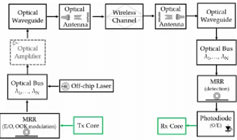
The source of the optical power at the transmitting link end can be an external off-chip laser coupled to the optical bus, emitting a nominal power PTX on the bus, steady in time according to the expected working temperature of commercial GPU/CPU architectures. Then, a dedicated micro ring resonator (MRR) can be used to provide both electrical-to-optical conversion and On–Off Keying (OOK) Non-Return-to-Zero (NRZ) amplitude modulation with a bandwidth Bopt over the optical carrier. The modulated signal is finally routed towards the optical antenna and wirelessly spread within the chip. As shown in the block scheme in Figure 2.2, an integrated optical amplifier may be present before the transmitting antenna, in order to cope with the large path loss coming
from the optical wireless channel and to push the received signal strength to the level required to drive the digital logic in the lower, electrical layer. Beyond the wireless channel, the optical incoming field is first gathered by the optical receiving antenna, then directed into the optical bus and finally filtered off by another MRR. A photodiode (PD) with responsivity ηPD reconstitutes the OOK signal in the electrical domain, ready to be demodulated.
Figure 2.2 Block scheme of the on-chip, optical wireless link
As long as the analysis is limited to a single link, symbols detection errors are due to the propagation impairments and to the noise effects experienced by the optical communication system. Since the thermal noise is often acknowledged as the dominant noise contribution , other noise sources like the PD shot noise and the relative intensity noise of the laser have been neglected herein. Conversely, in a multi-link scenario mutual interference among the different, simultaneous communications may arise, to an extent greatly dependent on antennas radiation properties, spacing and position. Although an effective implementation of O(Wi)NoC could benefit from this work involves no multiplexing scheme (e.g., simulations are run with only one WDM channel), in order to focus the investigations on the influence of antennas and core distances, excluding any issues above the physical layer.
20
Chapter-3
Fabrication Project
3.1 Dielectric and Plasmonic antennas
Dielectric Resonator Antennas (DRAs) are ceramic resonators that radiate energy into space when excited appropriately. Besides applications in antennas, these ceramic resonators are used in microwave circuits in areas such as filter and combiner applications. Usually they would be encased in a casing to prevent energy lost through radiation when used as such devices. The figures of merit for these resonators are their Q factor and temperature stability. The Q factor can range from 20 to 50000. The relative dielectric constant (,) for commercially available dielectric resonators (DRs) can range up to about an cr = 90. The temperature coefficients of resonant frequency (f) can range from about -6 to 4 ppm/°C.
An advantage of dielectric resonator antennas is they lack metal parts, which become lossy at high frequencies, dissipating energy. So these antennas can have lower losses and be more efficient than metal antennas at high microwave and millimeter wave frequencies. Dielectric waveguide antennas are used in some compact portable wireless devices, and military millimeter-wave radar equipment. The antenna was first proposed by Robert Richtmyer in 1939. In 1982, Long et al. did the first design and test of dielectric resonator antennas considering a leaky waveguide model assuming magnetic conductor model of the dielectric surface.
An antenna like effect is achieved by periodic swing of electrons from its capacitive element to the ground plane which behaves like an inductor. The authors further argued that the operation of a dielectric antenna resembles the antenna conceived by Marconi, the only difference is that inductive element is replaced by the dielectric material.
Contrary to traditional optical elements, Plasmonic antennas made from nanostructured metals permit the localization of electromagnetic fields on length scales much smaller than the wavelength of light. This results in huge amplitudes for the electromagnetic field close to the antenna being conducive for the observation of nonlinear effects already at moderate pump powers. Thus, these antennas exhibit a promising potential to achieve optical frequency conversion and all-optical
control of light at the nano-scale. This opens unprecedented opportunities for ultrafast nonlinear spectroscopy, sensing devices, on-chip optical frequency conversion, nonlinear optical metamaterials, and novel photon sources. The multi-level numerical approach proposed is virtually applicable to every optical antenna configuration, such as multiple-feed arrays of plasmonic antennas or dielectric antennas and to every multi-layered environment.
3.2. Optical Antennas
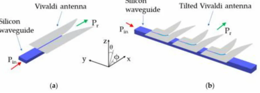
In order to evaluate the propagation and the performances of the wireless links in OWiNoC, different antenna configurations are considered. Actually, the antenna coupled to the optical waveguide is one of the key elements in the OWiNoC design as it allows to switch from wireless to wired optical propagation and vice versa. At the transmitting section, the antenna radiates in the surrounding medium the optical signal that comes from the input waveguide. The radiated signal propagates wirelessly and it is then transferred to an output waveguide by the receiving antenna. The analysis of propagation and performance of point-to-point optical wireless links carried out relies on the configurations of plasmonic antennas shown in Figure 3.1a, b, respectively.
Figure 3.1. Scheme of the single Vivaldi antenna (a) and of the tilted Vivaldi antenna array (b) coupled to a silicon waveguide
In particular, Figure 3.1a outlines the single antenna configuration, consisting of a silver plasmonic Vivaldi 1.75 µm long and 0.57 µm wide. The antenna is coupled to a silicon waveguide (0.38 µm × 0.22 µm) through a slotted plasmonic waveguide with length 1.63 µm. The optical signal (Pin) is launched into the Si waveguide and it is vertically coupled to a plasmonic slot waveguide, which is separated from the dielectric one by a dielectric layer. The antenna, obtained by shaping the plasmonic slot waveguide according to a Vivaldi profile, radiates the optical signal in the surrounding medium (PR) in the positive x direction. The behaviour is reciprocal when the antenna is used as receiver.
22
3.3 Fabrication Description
A sketch of the fabricated device is shown in Figure. 3.2. It has been designed to operate in the C-band (1530 nm1565 nm). and is based on the standard SOI technology. The structure is composed of a bottom layer of Silicon of thickness ℎ (𝐵) = 675 𝜇𝑚, an overlying layer of SiO2 of ℎ (𝑆) = 3 𝜇𝑚 height, and a further layer of Silicon of ℎ (𝐴𝑛𝑡) = 220 𝑛𝑚 thickness, where standard Si waveguides (with width 𝑤 (𝑊𝐺) = 480 𝑛𝑚) and the antennas are fabricated through Electron Beam Lithography (EBL). The antennas used for the considered links are realized by simply tapering the Si waveguides employing the same geometrical parameters presented in (Figure. 3.2a). Despite the not really compact dimensions, the narrow pattern on the horizontal (x-z) plane, together with the ease of manufacturing and high reliability, make this type of antenna suitable for the scope of this work, which is focused on the analysis of the effects of the propagation. As upper layer, the presence of SiO2 of 3 𝜇𝑚 thickness would represent the best solution, in order to have the dielectric antennas in the middle of an homogeneous layer bounded by air above and Silicon underneath, thus avoiding dielectric discontinuities close to the antennas. Unfortunately, the deposition of silica above the silicon waveguides and the antennas cannot guarantee a uniform surface at the top interface, preventing the possibility to control the propagation inside the chip. Indeed, surface uniformity is important to guarantee reproducibility in fabrication and to allow, through simulations, an effective design of the optical links.
Figure 3.2. 3D sketch (a) of the fabricated devices and layer structure of the sample in the x-y (b) and z-y (c) planes
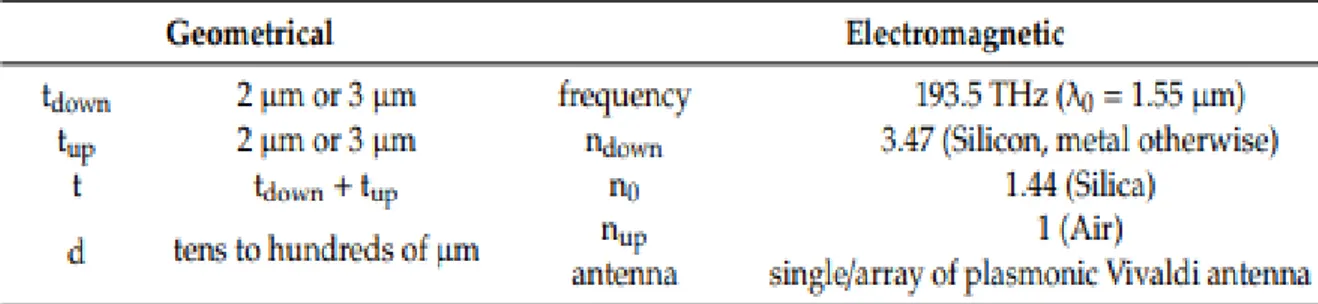
Therefore, after etching, Silicon waveguides and antennas have been covered with a thin layer (ℎ𝐴 = 300 𝑛𝑚) of borophosphorous tetraethyl orthosilicate (BPTEOS), which, contrarily to SiO2, can be planarized through annealing process, still owing a refractive index close to the one of Silica (see Table 3.1). Then, a polymer-based top layer made of UV26 of thickness ℎ𝑇 = 3.78 𝜇𝑚 and refractive index 𝑛𝑈𝑉26 = 1.526 has been further deposited above the BPTEOS. These two layers lead then to the presence of an overall quasi-homogenous medium, due to the close values of both refractive indices of these materials with the one of SiO2. Note that the sub-optimum solution of a single deposition of BPTEOS for a thickness of 3 𝜇𝑚 was not possible due to limitations in the maximum height of the coat allowed by the fabrication process. For this reason, the additional top layer has then been inserted. Among the different available polymers, the UV26 resulted to be the most suited because of the possibility of performing a single spin-coating phase of sufficient thickness, leading to a more uniform distribution of the material on the chip. Table 3.1 summarizes the electromagnetic and the geometrical properties of each layer.
24
Table 3.1 Layer Parameters
To demonstrate the presence of multi-path effects, various devices have been considered on the same wafer, with a link distance d between TX and RX antennas (Figure 3.2a) ranging from 20 𝜇𝑚 to 200 𝜇𝑚. In order to ease the input and output coupling of the optical signals, standard grating couplers were realized at waveguide terminations, and the same grating-to-grating length (2 mm) has been maintained for all the links. According to the EBL fabrication process, trenches are realized to pattern the waveguides and the antennas in the antenna layer. As shown in Figure. 3.2(b), these trenches create vertical discontinuities for the propagation on the horizontal x-z plane. To minimize the effects of possible lateral reflections on the received signal the trench width, 𝑤𝑇𝑟 in Figure. 3.2(a), has been chosen to be 𝑤𝑇𝑟 = 0.6 ⋅ 𝑑, according to results obtained through numerical simulations.
3.4 Optical Wireless Channel
According to the chip layered representation, the electromagnetic waves springing out from the on-chip transmitting antenna are expected to bounce onto the interfaces between the layers, thus triggering multipath effects .Assuming the antennas buried in a SiO2 layer limited by two different, unbounded media on the lower and on the upper side ,multipath is fundamentally generated by the multiple reflections between the interfaces (Figure 3.3) and can be evaluated by means of the Ray Tracing (RT) approach. It is worth pointing out that the RT modeling is particularly tailored to the investigation of the optical wireless channel, as geometrical optics is known to be an asymptotic theory, i.e., its accuracy increases at higher frequency.
Figure 3.3. Ray tracing evaluation of on-chip wireless propagation
Compared to other wireless networks, where the possible mobility of nodes and/or objects over quite large areas produces random-like fluctuations of the received signal intensity, the on-chip wireless channel is confined and static, as the chip layout is fixed and known beforehand. Therefore, propagation modeling at chip-level is quite well fit for characterization through deterministic approaches like RT, which require the prior knowledge of the physical environment. In order to run the RT simulation, both geometrical and electromagnetic properties of the link have to be set, the former referring to the SiO2 layer thickness (t in Figure 3.3), to the antennas distance from the interfaces (tup and tdown) and to the link distance (d0), the latter consisting of the materials refraction index (ndown, n0 and nup). A 3D representation of the antenna radiation patterns is also necessary as input file. The assessment can be carried out by embedding radiation diagrams into the RT tool, provided that they are encoded in the required format. Although propagation in Figure 3.3 is limited to the xz plane, a 3D description of the antenna patterns is nevertheless helpful, as the RT model can be then easily run regardless of the antenna orientation with respect to the propagation plane, e.g., for the assessment of the power received from an interfering transmitter. The geometrical/electromagnetic parameters considered herein for the RT simulations are summarized in Table 3.2.
26
Chapter-4
Measurements
Set Up
4.1 Experiment set up
Integrated circuits are often represented as layered structures, where the antennas are manufactured on / inside a SiO2 slab, laid on a silicon bulk and possibly covered by an upper passivation material. The outer package as well as possible heat sink and/or metal interconnects among the circuit elements may add further layers to the final stack.
According to the SOI technology, the chip structure is made by a bottom Si layer and by an overlying layer of SiO2. The antennas are fabricated on the top of the SiO2 substrate, and covered by a thin layer of borophosphorous tetraethyl orthosilicate (BPTEOS). Finally, a polymer-based top layer of UV26 is further deposited on the BPTEOS. As BPTEOS and SiO2 basically share the same refraction index, a single silica layer has been considered for RT simulations. During the measurement activities, the chip was placed on an aluminum stand, with air above the UV26 slab. Thickness and refraction index of the different materials are summarized in Table 4.1.
Table 4.1. Thickness and refraction index of the different materials
The experimental setup employed is shown in Figure 4.1. It consists of a tunable laser source (Yenista’s TLS Tunics T100) and a Yenista’s CT400 passive optical component tester, which allows to evaluate the transmission coefficient |𝑆21|^2 of the device under test (DUT) (i.e. the ratio between the measured received power and the output power produced by the port (O) of
28
the CT400) in the C-band. The use of an optical circulator also permits to measure the reflected power at the input port of the DUT, determining the reflection coefficient |𝑆11|^2. A polarization controller allows also to optimize the coupling from the fiber probe on the fundamental TE mode of the silicon waveguide.
Figure 4.1 Experimental setup
As previously described, fiber probes are coupled with the chip through taper gratings fabricated at the input/output sections of the waveguides, allowing an easy and repeatable coupling from the top side with an angle between the probes and the gratings of approximately 11 degrees. In order to exclude possible undesired temperature effects on the electrical and physical parameters of the DUT, the chip is placed on a Peltier cell, isolated in an Aluminum case, controlled with an external Thermo Electric Controller (TEC). The temperature of all the measurements is fixed at 25°C. To compensate for the losses and the wavelength response of external components, all measurements have been normalized with respect to a silicon reference waveguide of the same length fabricated on the same chip. This allows to directly obtain the link budget of the wireless connection only, which is therefore defined as:
𝐿𝑖𝑛𝑘 𝐵𝑢𝑑𝑔𝑒(𝑑𝐵) (𝑑) = |𝑆21(𝑑)| (𝑑𝐵)^2 − |𝑆21,𝑅𝑒𝑓| (𝑑𝐵)^2
where |𝑆21(𝑑)| (𝑑𝐵)^2 is the measured transmission coefficient of the DUT for different values of the distance between the antennas, while |𝑆21,𝑅𝑒𝑓| (𝑑𝐵)^2 represents the measurement related to the reference waveguide only. The measured values for the link
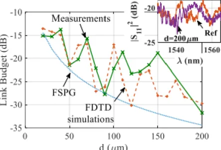
budget as a function of the distance d at = 1550 nm are shown in Figure 4.2. As inset, the measured reflection coefficients |𝑆11| (𝑑𝐵)^2 for the reference waveguide (red curve) and for 𝑑 = 200 𝜇𝑚 antenna link (violet curve) are reported. These curves confirm that the antenna fabricated is well matched in the whole wavelength range of the C-band, since no appreciable difference is observed with respect to the |𝑆11|^2 measured on the reference waveguide. The same behavior was verified for all the link distances.
Measurements are compared in Figure 4.2 with FDTD simulations and with the theoretical free space path gain (FSPG) computed using the well-known Friis equation: 𝐹𝑆𝑃𝐺 = 𝐺t𝐺r ( 𝜆 /4𝜋𝑑𝑛(𝑆𝑖𝑂2))^2. It is shown that simulations are in good agreement with the experimental results confirming, the presence of multi-path propagation likely due to the multi-layer layout shown in Figure 4.2 (fabrication)
Figure 4.2 Measured values of the link distance as a function of = 1550 nm
4.2 Assessment of Optical Wireless Networks-on-Chip
The performance of a communication link is often characterized in terms of bit error probability (BEP). In a binary, optical communication system, BEP can be defined as the probability that the received photocurrent transmitting 0 is detected above the decision threshold, or it is detected below the threshold while transmitting 1. BEP is usually experimentally assessed or estimated by means of analytical formulas for single link, which can be computed based on the estimated value of the received power after the photodiode. However, wireless network design always requires a careful study of cross-link interferences, which may occur among simultaneously links exploiting the same (optical) channel. In fact, the spatial reuse of optical wavelengths improves
30
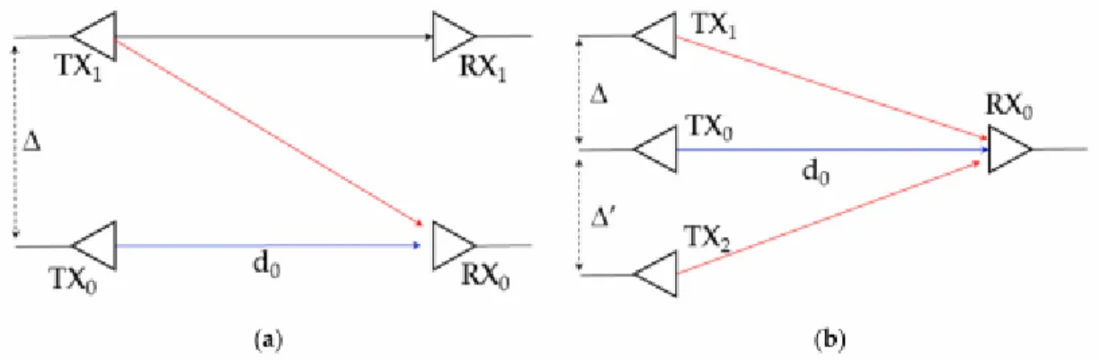
significantly the transport capacity in OWiNoC, since the number of simultaneous communications will not be limited by the number of available wavelengths. On the other hand, wavelength reuse can trigger co-channel interference, which can harshly degrade the system performance, if not effectively handled and mitigated. Hence, the design of OWiNoC can greatly benefit from an interference-aware framework for BEP evaluation. Compliance of different link configurations with the target performance for the on-chip communication can be investigated. In a general OWiNoC scenario, I + 1 transmitters using the same optical wavelength can be present, with only one useful transmitter TX0 for the desired receiver RX0 and the other I transmitters (TX1, TX2, . . . , TXI ) causing interference to RX0 while communicating with their corresponding receivers. The optical power (i.e., the power of the unmodulated optical carrier) of the received desired signal is here denoted by P0, and the normalized optical power of the i-th received interfering signal is denoted by xi = Pi /P0, with i = 1, 2, . . . , I. The received power values depend on the radiation properties of the antennas, their spacing and orientation and on the propagation characteristics of links. In the former case (Figure 4.3a), two parallel links, separated by the distance ∆, carry data in the same direction up to a distance d0. The optical signal from TX0 to RX0 is exposed to the interference of the signal coming from TX1, which may therefore affect the communication BEP. In the latter scenario (Figure 4.3b), an additional, parallel, interfering link is introduced at a distance ∆’ from the reference link TX0–RX0.
Figure 4.3. Optical Wireless Networks-on-Chip scenario with a single (a) and with two (b), parallel interfering link(s).
For each OWiNoC scenario, the received powers can be evaluated with FDTD or RT tools. For a given transmitted optical input power Pin, the received power can be computed as Pi = PGi ·Pin, where PGi is the path gain of the channel between the i-th transmitter and the reference receiver RX0.
Chapter-5
Propagation
Modelling
The different configurations of the antennas considered for the varying distances from 20 𝜇𝑚 to 200 𝜇𝑚 which are as given below:
Figure 5.1 Point to Point link antenna configuration
The simple point to point direct link is shown in the Figure 5.1 which consist of a transmitting antenna and a receiving antenna with varying link distance d(𝜇𝑚).
Figure 5.2 Point to Point link antenna configuration with reference path
The simple point to point direct link is shown in the Figure 5.2 which consist of a transmitting antenna and a receiving antenna along with the reference waveguide with varying link distance d(𝜇𝑚).
32
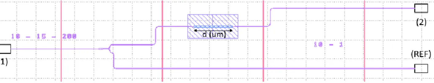
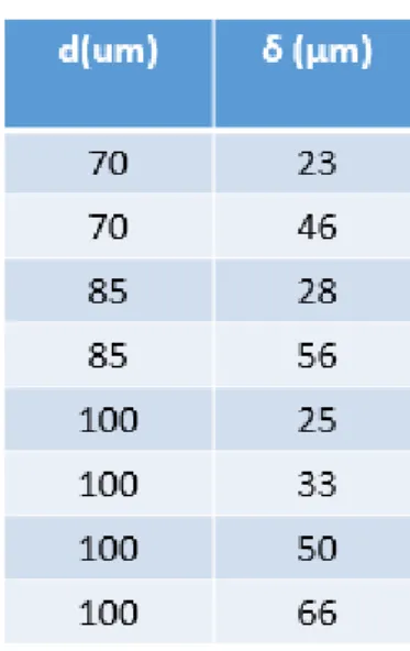
Figure 5.3 Point to point antenna configuration with cross waveguide
In Figure 5.3, a cross waveguide is introduced in between the transmitting and receiving antennas with varying link distance d (𝜇𝑚) and also with varying distance between transmitting antenna and the cross waveguide δ WG (𝜇𝑚) as given in Table 5.1.
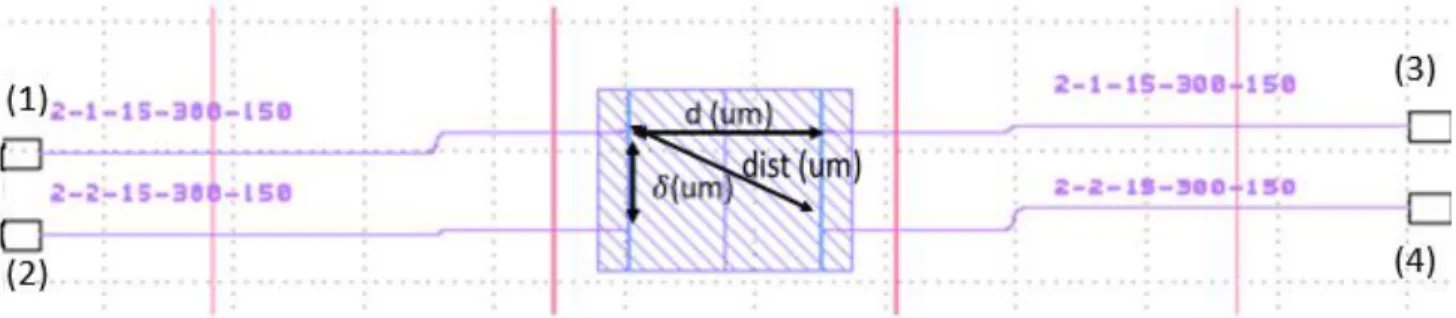
Figure 5.4 1x3 Antenna configuration
In Figure 5.4, a single transmitter and three receivers are considered with varying link distance between the transmitting and receiving antennas (d (𝜇𝑚) and dist. (𝜇𝑚)) as given in Table 5.2.
Table 5.2 Measured values for 1x3 Antenna configuration
34
In Figure 5.5, two transmitting and two receiving antennas are considered with varying link distance between the transmitting and receiving antennas (d(𝜇𝑚) and dist(𝜇𝑚)) as given in Table 5.3.
Table 5.3 Measured values for 2x2 Antenna configuration
Figure 5.6 2x2 Cross Antenna configuration
In Figure 5.6, two transmitter and two receiver antennas are considered perpendicular with each other with varying link distance between the transmitting and receiving antennas (d(𝜇𝑚) .
The performance of the RT tool for the channel modelling of OWiNOC have been done with different Propagation modelling. In order to reduce the complexity of the simulations, they have been carried out under the following assumptions:
1. the difference between BPTEOS and SiO2 has been neglected, taking a single layer with n=1.445 and thickness equal to 3.3 m (m+k in Figure 5.7) has been considered;
2. the “trenches” have been also neglected, i.e. each layer has been assumed transversally unbounded;
3. as far as their transmission/reception properties are concerned, the antennas can be regarded as point-sources placed in the middle of the taper aperture area, i.e. at 3.11 m from the Si-SiO2 interface
Figure 5.7 Sketch of the Layer stack
The Layer stack shown in Figure 5.7 is the same as described in the Figure 3.2 (b).
Figure 5.8 Simple mode propagation model
Simple mode (Highest Simplification): the UAV is also supposed equal to SiO2, and therefore the antennas are buried in a silica layer 7.08 m (m+k+r) in Figure 5.8. The bottom silicon layer is not limited underneath.
36
Figure 5.9 Enhanced mode (only upper layer) propagation model
Enhanced mode (Middle Simplification, MS): the UAV layer is introduced on top of the SiO2. The lowest silicon layer is still unbounded.
Figure 5.10 Enhanced mode propagation model
Enhanced mode (Lowest Simplification, LS): a metal (aluminium) – silicon interface is added to take into account the finite thickness (675 m approximately) of the silicon layer.
Simulations have been run through a ray tracing simulation tool specifically conceived in Matlab (MRT) to investigate wireless propagation in layered medium.
As pointed out, in its original formulation it basically consists of simple, closed form analytical formulas which can easily manage the simplest scenario in Figure 5.8, and more in general any situations where the antennas are included within a layer limited by two unbounded media (2 interfaces). The model has been then extended to account for a further higher/lower layer of finite thickness (UAV and/or silicon) , where electromagnetic reflection by a slab is modelled by means of “enhanced” reflection coefficients, which take into account the multiple bounces setting up within the layer.
It is worth pointing out the need to modify the formulas to consider the possibility of different materials on the opposite sides of the reflecting layers (SiO2 and Air for the UAV layer, and SiO2 and Aluminium for the Si layer). Rays undergoing two/four refractions across the upper/lower layers can be still analytically managed, although the analytical formulation becomes increasingly complex. In order to limit the complexity, just some of all the refracted rays can be managed. Because of its analytical formulation, the MRT is quite computationally effective, and therefore it can manage a very large number of reflection at the interfaces bounding the silica layer in a quite short computation time. Transmission model is also considered. All the simulations are carried out with tuned antennas as well as with antennas which are not tuned.
38
Chapter-6
Measurements and Simulation Results
In order to check the performance of RT for channel modeling in OWiNoC, RT simulations have been carried out in a layered environment with geometrical and electromagnetic parameters as in Table 3.1. The radiation properties of the tapered antennas have been investigated by means of FDTD simulations, and the - and - components of the spatially radiated electric field have been stored in an input file for the ray tool. The communication wavelength is 0=1.55m (corresponding to a frequency f0193.55THz) and the link distance ranges from 20m to 1500m, with receivers placed in between.
In order to set a suitable number of reflections in the RT tool, the root mean square difference (RMSD) between simulations with reflection orders respectively equal to m and (m+5) has been computed. According to Fig. 6.1, at least 50 reflections seem necessary to have a RMSD value lower than 1 dB for both the “full ray” and the “enhanced reflection” approaches, thus corroborating the presence of strong multipath inside the environment.
Figure 6.1 Prediction for the Enhanced and Simple mode models and comparison with measured data for a Point to point antenna
Figure 6.2 Prediction for the Enhanced and Simple mode models and comparison with measured data for a Point to point antenna with reference waveguide
Figure 6.3 Prediction for the Enhanced and Simple mode models and comparison with measured data for a Cross waveguide model
40
Figure 6.4.1. Prediction for the Simple mode model and comparison with measured data for a 1x3 antenna configuration with 1-1 direct link
Figure 6.4.2 Prediction for the Simple mode model and comparison with measured data for a 1x3 antenna configuration with 1-toplink
Figure 6.4.3. Prediction for the Simple mode model and comparison with measured data for a 1x3 antenna configuration with 1-bottom link
Figure 6.4.4 Prediction for the Enhanced mode model and comparison with measured data for a 1x3 antenna configuration 1-1direct link
42
Figure 6.4.5 Prediction for the Enhanced mode model and comparison with measured data for a 1x3 antenna configuration 1-toplink
Figure 6.4.6 Prediction for the Enhanced mode model and comparison with measured data for a 1x3 antenna configuration 1-1bottom link
Figure 6.5.1 Prediction for the Simple mode model and comparison with measured data for a 2x2 antenna configuration with 1-3direct link
Figure 6.5.2 Prediction for the Simple mode model and comparison with measured data for a 2x2 antenna configuration with 1-bottom link
44
Figure 6.5.3 Prediction for the Simple mode model and comparison with measured data for a 2x2 antenna configuration with 2-4 direct link
Figure 6.5.4 Prediction for the Simple mode model and comparison with measured data for a 1x3 antenna configuration with 2-3 link
Figure 6.5.5 Prediction for the Enhanced mode model and comparison with measured data for a 2x2 antenna configuration with 1-3direct link
Figure 6.5.6 Prediction for the Enhanced mode model and comparison with measured data for a 2x2 antenna configuration with 1-down link
46
Figure 6.5.7 Prediction for the Enhanced mode model and comparison with measured data for a 2x2 antenna configuration with 2-4direct link
Figure 6.5.8 Prediction for the Enhanced mode model and comparison with measured data for a 2x2 antenna configuration with 2-3up link
Figure 6.6.1 Prediction for the Simple and Enhanced mode model and comparison with measured data for a 2x2 cross antenna configuration with 1-1 link
Figure 6.6.2 Prediction for the Simple and Enhanced mode model and comparison with measured data for a 2x2 cross antenna configuration with 2-2link
48
In Table 6.1, the root mean square error (RMSE) together with the mean value and the standard deviation between measurements and simulations is presented. Results highlight that taking into account only reflections leads to completely unreliable predictions and refractions have to be embedded into the RT tool as they seem to play a dominant role, at least in the investigated scenario.
Table 6.1 Measured values for mean, standard deviation and RMSE for antennas not tuned
Taper
(antennas not tuned)
Mean
Error (dB) err (dB) RMSE (dB)
Vivaldi
(antenn as not tuned)
Mean
Error (dB) err (dB) RMSE (dB)
Simple mode 6.26376 3.073571429 5.45783 9.97419080 7.77893 6.24282 Enhanced 7.357882314 2.41893 6.9489 11.9248478 7.4725 9.293209 Enhanced only upper level 9.110751492 4.71643 7.7949403 8.52830287 0.19286 8.526121986 Transmission model 7.912985 2.372857 7.548833 11.39153 7.065 8.936039
Table 6.1 Measured values for mean, standard deviation and RMSE for tuned antennas
It is worth noting that although the simple mode model seems quite close to measurements in Figure. , the accuracy is still weak (RMSE = 5.45783dB in Table 6.1), the reason being that it is mostly impossible to match actual fast-fading with simulations, because of unavoidable imprecisions in the description of either the propagation environment or the antennas.
A spatial filtering has been then carried out to overcome fast fading issues, aiming at assessing path gain average range dependence in measurements and simulations. Comparison between the RT approaches and measurement is reported Table 6.2 for Tuned antennas. The full ray RT model is more reliable with respect to the enhanced reflection approach t can provide a better estimate of the path-loss exponent in the optical wireless channel.
Of course, running a full ray simulation requires a heavier computation effort, as the number of rays to be traced is much greater (about 9 million rays against less than 1.5 million for the “enhanced” approach). The different computational burden clearly affects the simulation time, equal to few hours on standard PCs for the full ray model, whereas it drops to some seconds for the simplified model. It is worth pointing out that general purpose RT tools would take much longer time to track such a huge number of paths.
Taper
Mean
Error (dB) err (dB) RMSE dB)
Vivaldi
Mean
Error (dB) err (dB) RMSE (dB)
Simple mode 6.77456 0.03536 6.77447 8.05107 4.7275 6.53495 Enhanced 7.24788 4.57857 5.61858 12.0063 9.27071 7.86198 Enhanced only upper level 2.6027984939 2.09214 6.2529 9.48937 6.78429 6.63488 Transmission model 8.778119 0.34786 8.771224 11.27385 4.344286 10.40321
50
Conclusion
Optical wireless networks-on-chip are investigated in this thesis by means of simulations carried out in some reference cases and according to a multi-level analysis, taking into account the main factors simultaneously affecting the performance of the on-chip, point-to-point communication. In particular, bit error-probability and communication range have been assessed in relation to the antenna radiation properties, the geometry and the constituting material of the chip, the mutual position of the interfering links. A suitable ray tracing tool for optical wireless networks on chip has been set up aiming at simulating the optical wireless channel for intra-chip links design. The on-chip scenario is a layered environment where, at optical frequencies, the communication link distance is hundred and even thousand times the layers thickness. Therefore, the wireless channel is dominated by multipath and a high number of reflections/refractions has to be taken into account for a reliable prediction. Comparisons between measurements and simulations show that reflections outside the antenna layer play a key role, at least in the investigated case. Refracted rays have been taken into account through a “full ray” approach or embedded into modified reflection coefficients. In the former case overall good agreement can be reached for the average path gain range dependence, whereas it is not as much satisfactory in the latter. Point specific field prediction is indeed quite worse in both cases, as fast fading tracking accuracy is limited by unavoidable uncertainties and errors in the antenna digital description and/or in the representation of the propagation environment. As the ray tracing algorithm is tailored to layered scenarios, full ray simulations take few hours to track several millions of rays, i.e. the model is quite faster than general purpose ray tools. It allows a set of tools permitting the design and the performance evaluation of on-chip wireless optical communications as a function of the main parameters of the link components and geometries, including the presence of interference from other transmitters, opening the possibility to design new architectures for many-core and kilo-core CMPs.
Bibliography
[1] F. Fuschini, M. Barbiroli, M. Zoli, G. Bellanca, G. Calò, P. Bassi, V. Petruzzelli “Ray tracing modeling of electromagnetic propagation for on-chip wireless optical communications”, Journal of Low Power Electronics and Applications, vol. 8, No. 4, December 2018, DOI: 10.3390/jlpea8040039
[2] W.D. Burnside, K.W. Burgener, “High Frequency Scattering by a Thin Lossless Dielectric Slab”, IEEE Trans. on Antennas and Propagation, vol. 31, No. 1, January 1983.
[3] IEEE TRANSACTIONS ON ANTENNAS AND PROPAGATION, VOL.
AP-31, NO. 1, JANUARY 1983
[4] J. Nanni et al., “Multi-Path Propagation in On-Chip Optical Wireless Links”, IEEE Photonics Tech. Letters, vol. 32, no. 17, September 2020;
[5] G. Calò et al., “Assessment of On-chip Wireless Communication Networks Based on Integrated Dielectric Antennas”, 22nd Int. Conf. on Transparent Optical Networks”, Bari (IT), July 19-23, 2020;
[6] Shuai Wang, Tao Jin “Wireless network on chip : a survey”, The Journal of Engineering. [7] Dielectric Resonator Antennas; theory and design Author(s) Lim, Beng- Teck, 1974
[8] Calò, G.; Alam, B.; Bellanca, G.;Fuschini, F.; Barbiroli, M.; Tralli, V.; Bassi, P.; Stomeo, T.; Bozzetti, M.; Kaplan, A.E ; et ak. Dielectric and Plasmonic Vivaldi Antennas for On-Chip Wireless Communication. In Proceedings of the 21st International Conference on Transparent Optical Networks, Angers , France, 9-13 July 2019.
[9] Shafiei Dehkordi, J.; Tralli, V. Interference Analysis for Optical Wireless Interconnections. In Proceedings of the 29th IEEE International Symposium on Personal, Indoor and Mobile Radio Communications, Bologna, Italy, 9–12 September 2018.
[10] Shafiei Dehkordi, J.; Tralli, V. Interference Analysis for Optical Wireless Communications in Network-on-Chip Scenarios. IEEE Trans. Commun. (Early Access) 2019.
[11] F. Fuschini et al., "Multi-Level Analysis of On-Chip Optical Wireless Links," in Appl. Sci., Vol. 10, no. 1, art no.196, 2020.
[12] G. Bellanca, G. Calò, A.E. Kaplan, P. Bassi and V. Petruzzelli, "Integrated Vivaldi plasmonic antenna for wireless on-chip optical communications," in Optics Express, vol. 25, no. 14, pp. 16214-16227, 2017.
52
[13] M. Nafari, L. Feng and J. M. Jornet, "On-Chip Wireless Optical Channel Modeling for Massive Multi-Core Computing Architectures," 2017 IEEE Wireless Communications and Networking Conference (WCNC), San Francisco, CA, 2017, pp. 1-6, doi: 10.1109/WCNC.2017.7925962.
[14] S. Deb, A. Ganguly, P.P. Pande, B. Belzer, D. Heo, “Wireless NoC as Interconnection Backbone for Multicore Chips: Promises and Challenges”, IEEE J. Emerg. Sel. Top. Circuits Syst., vol. 2, no. 2, June 2012;